Application Note: AN_SY7066/SY7066A
1.8V Minimum Input and 5. 5V Maximum Output
6A Peak Current Synchronous Boost with Output Disconnect
Features
General Description
SY7066/SY7066A is a high efficiency synchronous
boost regulator that converts down to 1.8V input and
up to 5.5V output voltage. It adopts NMOS for the
main switch and PMOS for the synchronous switch. It
can disconnect the output from input during the
shutdown mode.
Ordering Information
SY7066 □(□□)□
•
Temperature Code
Package Code
Optional Spec Code
Ordering Number
SY7066QMC
SY7066AQMC
Package type
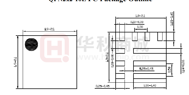
QFN2X2-10
QFN2X2-10
•
•
•
•
•
•
•
•
•
Note
-------
1.8V Minimum input voltage
Adjustable output voltage from 2.5V to 5. 5V
6A peak current limit
Input under voltage lockout
Load disconnect during shutdown
Output over voltage protection
Input battery voltage monitor
Low RDS(ON) (main switch/synchronous switch)
at 5.0V output: 20/40mohm
Automatic output discharge at shutdown:
ο SY7066: Auto output discharge function
ο SY7066A: No output discharge function
Compact package: QFN2x2-10
Applications
•
All Single Cell Li or Dual Cell Battery
Operated Products as MP-3 Player, PDAs, and
Other Portable Equipment.
Typical Applications
Figure 1. Schematic Diagram
AN_SY7066/A Rev. 0.9B
Figure 2. Efficiency Figure
Silergy Corp. Confidential- Prepared for Internal Use Only
1
�AN_SY7066/A
Pinout (top view)
(QFN2X2-10)
Name
PVOUT
SVOUT
LX
PGND
SGND
IN
EN
LBI
FB
LBO
Top mark: MGxyz for SY7066 (Device code: MG., x=year code, y=week code, z= lot number code)
Aaxyz for SY7066A (Device code: Aa., x=year code, y=week code, z= lot number code)
QFN2X2-10
Description
1
Power output pin. Decouple this pin to GND pin with at least 22uF ceramic cap.
Signal output pin. Decouple this pin to GND pin with at least 1.0uF ceramic cap for noise
6
immunity consideration.
2
Inductor node. Connect an inductor between IN pin and LX pin.
3
Power ground pin.
4
Signal ground pin.
5
Signal input pin.
7
Enable pin. Internal integrated with 1Mohm pull down resistor.
8
Low battery comparator input.
Feedback pin. Connect a resistor R1 between OUT and FB, and a resistor R2 between FB
10
and GND to program the output voltage. VOUT=1.2V*(R1/R2+1).
9
Low battery comparator output.(open drain) .
Absolute Maximum Ratings (Note 1)
EN-----------------------------------------------------------------------------------------------------------------------VOUT+0.3V
Other Pins------------------------------------------------------------------------------------------------------------------- 6V
Power Dissipation, PD@ TA=25°C QFN2x2-10------------------------------------------------------------------------2.5W
Package Thermal Resistance (Note 2)
θ JA ---------------------------------------------------------------------------------------------------------------50°C/W
θ JC ---------------------------------------------------------------------------------------------------------------10°C/W
Junction Temperature Range --------------------------------------------------------------------------------------------- 150°C
Lead Temperature (Soldering, 10 sec.) --------------------------------------------------------------------------------- 260°C
Storage Temperature Range ---------------------------------------------------------------------------------- -65°C to 150°C
Recommended Operating Conditions (Note 3)
IN ------------------------------------------------------------------------------------------------------------------ 1.8V to 5.25V
PVOUT, SVOUT------------------------------------------------------------------------------------------------- 2.5V to 5.5V
EN ---------------------------------------------------------------------------------------------------------------- 0V to VOUT+0.3V
All other pins ------------------------------------------------------------------------------------------------------------- 0-5.5V
Junction Temperature Range ---------------------------------------------------------------------------------- -40°C to 125°C
Ambient Temperature Range ----------------------------------------------------------------------------------- -40°C to 85°C
AN_SY7066/A Rev. 0.9B
Silergy Corp. Confidential- Prepared for Customer Use Only
2
�AN_SY7066/A
Electrical Characteristics
(VIN =2.4V, VOUT=5V, IOUT=500mA, TA = 25°C unless otherwise specified)
Parameter
Input Voltage
Output Voltage Range
Quiescent Current VIN
VOUT
Shutdown Current
Linear charge current
Symbol
VIN
VOUT
IQ
Soft-start time
Input Vin UVLO threshold
Vin UVLO hysteresis
EN Rising Threshold
EN Falling Threshold
LBI Voltage Threshold
LBI Input Hysteresis
Low Side Main FET RON
Synchronous FET RON
Main FET Current Limit
Switching Frequency
Feedback Reference Voltage
Output over voltage protection
Minimum on time
Minimum off time
Max on time
Thermal Shutdown Temperature
Thermal Shutdown hysteresis
Output Discharge Resistor
Tss
VUVLO
VHYS
VENH
VENL
VLBI
VLBI_HYS
RDS(ON)1
RDS(ON)2
ILIM1
fsw
VREF
VOVP
TON_MIN
TOFF_MIN
TON_MAX
TSD
THYS
RDSC
ISHDN
ICHARGE
Test Conditions
Min
1.8
2.5
Io=0A,VEN=VIN=1.8V,
VOUT=5.0V
VEN=0V, VIN=2.4V
VOUT≤1V
1V
很抱歉,暂时无法提供与“SY7066AQMC”相匹配的价格&库存,您可以联系我们找货
免费人工找货