CMD75N04/CMU75N04
N-Channel Enhancement Mode MOSFET
General Description
Product Summary
The 75N04 uses innovative
BVDSS
RDSON
ID
40V
7.5mΩ
75A
packaging technology to provide
excellent RDS(ON). This device
Applications
is suitable for use as a wide variety
DC/DC converter
of applications.
Powertrain Management
Solenoid and Motor Drivers
Features
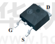
TO-252/251 Pin Configuration
N-channel Enhancement mode
D
Low On-Resistance
100% Avalanche tested
G
S
RoHS Compliant
TO-252
(CMD75N04)
G
D
S
TO-251
(CMU75N04)
Absolute Maximum Ratings
Symbol
Parameter
Rating
Units
VDS
Drain-Source Voltage
40
V
VGS
Gate-Source Voltage
±20
V
ID@TC=25℃
Continuous Drain Current
75
A
ID@TC=100℃
Continuous Drain Current
53
A
IDM
Pulsed Drain Current
300
A
EAS
Single Pulse Avalanche Energy
200
mJ
PD@TC=25℃
Total Power Dissipation
60
W
TSTG
Storage Temperature Range
-55 to 175
℃
TJ
Operating Junction Temperature Range
-55 to 175
℃
Thermal Data
Symbol
Parameter
RθJA
Thermal Resistance Junction-ambient
RθJC
Thermal Resistance Junction -Case
CA01S1
www.cmosfet.com
Typ.
Max.
Unit
---
62
℃/W
---
2.6
℃/W
Page 1 of 2
�CMD75N04/CMU75N04
N-Channel Enhancement Mode MOSFET
Electrical Characteristics (TJ=25℃ , unless otherwise noted)
Symbol
BVDSS
RDS(ON)
VGS(th)
Parameter
Drain-Source Breakdown Voltage
Static Drain-Source On-Resistance
Gate Threshold Voltage
Conditions
Min.
Typ.
Max.
Unit
V
VGS=0V , ID=250μA
40
---
---
VGS=10V , ID=20A
---
6.5
7.5
VGS=4.5V, ID=20A
---
8
11
VGS=VDS , ID =250uA
1
---
3
VDS=40V , VGS=0V , Tj =25℃
---
---
1
VDS=18V , VGS=0V , Tj =85℃
---
---
20
±100
nA
mΩ
V
uA
IDSS
Drain-Source Leakage Current
IGSS
Gate-Source Leakage Current
VGS =±20V , VDS=0V
---
---
gfs
Forward Transconductance
VDS=5 V , ID=20A
---
30
---
S
---
2
---
Ω
---
25
33
---
12
---
---
3.5
---
Rg
Gate Resistance
Qg
Total Gate Charge
Qgs
Gate-Source Charge
Qgd
Gate-Drain Charge
Td(on)
Tr
Td(off)
Tf
VDS=0V , VGS=0V , f=1MHz
VDD=32V , VGS=0 to 10V, ID=75A
Turn-On Delay Time
---
7
---
Rise Time
VDD=20V , VGS =10V , RG=3.5Ω
---
10
---
Turn-Off Delay Time
ID =75A
---
6
---
nC
ns
Fall Time
---
8
---
Ciss
Input Capacitance
---
2400
---
Coss
Output Capacitance
---
490
---
Crss
Reverse Transfer Capacitance
---
15
---
Min.
Typ.
Max.
Unit
---
---
1.2
V
VDS=25V , VGS=0V , f=1MHz
pF
Diode Characteristics
Symbol
VSD
Parameter
Diode Forward Voltage
Conditions
VGS=0V , IF = 20A
Note :
1.The test condition is VDD=20V,VGS=10V,L=0.5mH,I AS=28A
This product has been designed and qualified for the counsumer market.
Cmos assumes no liability for customers' product design or applications.
Cmos reserver the right to improve product design ,functions and reliability wihtout notice.
CA01S1
www.cmosfet.com
Page 2 of 2
�
很抱歉,暂时无法提供与“CMD75N04”相匹配的价格&库存,您可以联系我们找货
免费人工找货- 国内价格
- 5+1.37207
- 50+1.08357
- 150+0.95982
- 500+0.80562
- 2500+0.70825
- 5000+0.66701