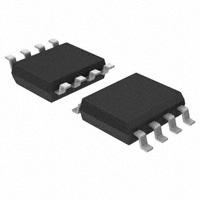
W83310S/W83310SG
Winbond
Bus Termination Regulator
With
Over Temp. & Current Limit
Protection
W83310S
W83310SG
�W83310S/W83310SG
W83310S
Datasheet Revision History
PAGES
1.
VERSION
MAIN CONTENTS
DATES
VERSION
Oct./03
0.5
N.A.
All versions before 0.5 are for internal use
only.
ON WEB
2.
3,9
Oct./03
0.51
N.A.
AC spec. and typical waveform update.
3
12
Feb./04
0.60
N.A.
Add the thermal data.
4
3
Jul./04
0.61
N.A.
Add min./typ. value of VIN.
5
2,3,11
Jan./06
0.7
N.A
Modify application circuit, AC characteristic
and add Pb-free part no: W83310SG.
6
13
Oct./06
1.0
N.A
Update ordering information and official
release of version 1.0
-I-
Publication Release Date: Oct. 2006
Revision 1.0
�W83310S/W83310SG
Table of Contents1.
GENERAL DESCRIPTION ......................................................................................................... 1
2.
FEATURES ................................................................................................................................. 1
3.
APPLICATIONS .......................................................................................................................... 1
4.
PIN CONFIGURATION AND DESCRIPTION ............................................................................ 2
5.
APPLICATION CIRCUIT............................................................................................................. 3
6.
INTERNAL BLOCK DIAGRAM- W83310S ................................................................................. 4
7.
ELECTRICAL CHARACTERISTICS........................................................................................... 5
7.1
AC CHARACTERISTICS................................................................................................ 5
8.
TYPICAL OPERATING WAVEFORM......................................................................................... 6
9.
PACKAGE DIMENSION (POWER SOP-8) .............................................................................. 12
10.
THERMAL PERFORMANCE.................................................................................................... 13
11.
ORDERING INFORMATION .................................................................................................... 13
12.
HOW TO READ THE TOP MARKING...................................................................................... 13
-II-
�W83310S/W83310SG
1. GENERAL DESCRIPTION
The W83310S is a linear regulator which provides achieves continuous 1.8 Amp bi-directional sinking
and driving capability for DDR SDRAM bus terminator application. The chip simply implement a stable
power supply which can track half of input power dynamically for bus terminator with a single chip; that
is the chip integrates two power MOSFETs. There is no any external power device needed. The
W83310S is promoted with SOP-8 power package. With W83310S design, a high integration, high
performance, and cost-effective solution is promoted.
2. FEATURES
y
Regulates a bi-directional power with driving and sinking capability
y
Provides achieve continuous 1.8Amp driving and sinking current
y
Power MOSFET integrated
y
Low external component count
y
Low output voltage offset
y
Operates with +3.3V and +2.5V control power
y
Current limit protection
y
Over temperature protection
y
Power package SOP-8
y
Low cost and easy to use
3. APPLICATIONS
y
DDR and DDR II Bus Termination Regulator
y
Active Termination Bus
y
SSTL-2
y
SSTL-3
-1-
Publication Release Date: Oct. 2006
Revision 1.0
�W83310S/W83310SG
4. PIN CONFIGURATION AND DESCRIPTION
VIN
1
GND
2
VREF
3
VOUT
4
8 NC
inbond
W83310S
7 NC
6 VCNTL
5 NC
SYMBOL
PIN
FUNCTION
VIN
1
Power input pin.
GND
2
Ground.
VREF
3
Reference voltage and Chip enable.
VOUT
4
Output voltage.
NC
5
No function
VCNTL
6
Gate drive voltage.
NC
7
No function
NC
8
No function
-2-
�W83310S/W83310SG
5. APPLICATION CIRCUIT
2.5VSTR
2.5VSTR/VCC3
U1
VIN
R1
100K
C1
1000u
3
1
2N7002
2
3.3VDL/VCC3
GND
NC
VREF
Q1
ENABLE#
NC
R2
100K
C2
1u
VCNTL
VOUT
R4
1K
C4
1u
C5
1000u
NC
W83310S/SG
R3
1K
C3
1u
Note:
R4=1 Kohm reserve for VOUT discharge or sink internal bias when VIN is not present but VCNTL is present.
R3=1 Kohm reserve for sink internal bias when VCNTL is not present but VIN is present.
-3-
Publication Release Date: Oct. 2006
Revision 1.0
�W83310S/W83310SG
6. INTERNAL BLOCK DIAGRAM- W83310S
VCNTL
VIN
Current
Limit &
OTP
Control
VREF
Logic
Circuit
GN
-4-
VOUT
�W83310S/W83310SG
7. ELECTRICAL CHARACTERISTICS
7.1
AC CHARACTERISTICS
W83310S
VIN=2.5V,VCNTL=3.3V,VREF=1.25V,COUT=100UF, TA = 0°C TO +70°C
PARAMETER
Output Offset Voltage
SYMBOL
MIN
VOS
Load Regulation
Input Voltage Range
Operating Current of
VCNTL
Operating Current of VIN
TYP
MAX
UNITS
-20
20
mV
-20
20
-20
20
IOUT=0A
Loading: 0AÆ2.0A
mV
Loading: 0AÆ2.0A
2.5/1.8
3.63
VCNTL
3.3
3.63
IVCNTL
1
1.5
mA
No Load(IOUT=0A)
1
mA
No Load(IOUT=0A)
VIN
1.7
TEST
CONDITIONS
IVIN
0.8
Shutdown Threshold
Trigger
0.2
50
Shutdown Current of VIN
ISHDN
Short Current Limit
ILMT
4
Over Temperature
Protection
OTP
130
V
V
Output=High
V
Output=Low
uA
A
145
VREF
很抱歉,暂时无法提供与“W83310SG TR”相匹配的价格&库存,您可以联系我们找货
免费人工找货