SLG5NT1462V
Ultra-small Dual 40 mΩ 1.0 A
Integrated Power Switch with Discharge
General Description
Pin Configuration
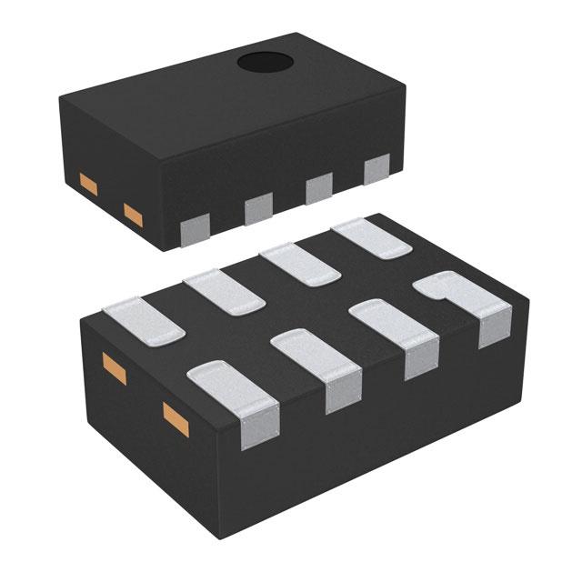
The product is packaged in an ultra-small 1.6 x 1.0 mm package.
Features
•
•
•
•
•
•
•
Two 40 mΩ 1.0 A MOSFETs
Two integrated VGS Charge Pumps
User selectable ramp rate with external resistor
Protected by thermal shutdown
Integrated Discharge Resistor
Pb-Free / Halogen-Free / RoHS compliant
STDFN 8L, 1.0 x 1.6 mm
D2
1
ON2
2
ON1
3
D1
4
SLG5NT1462V
The SLG5NT1462V is designed for power switching applications. The part comes with two 40 mΩ 1.0 A rated MOSFETs,
each controlled by an ON control pin. Each MOSFET’s ramp
rate is adjustable depending on the input current level of the
ON pin.
8
S2
7
GND
6
VDD
5
S1
8-pin STDFN
(Top View)
Block Diagram
S1
D1
D2
S2
1.0 A
1.0 A
VDD
2.5 V to 5.5 V
Charge
Pump Out
Charge
Pump Out
ON1
ON2
CMOS Input
GND
Silego Technology, Inc.
000-005NT1462-103
Rev 1.03
Revised December 4, 2015
�SLG5NT1462V
Pin Description
Pin #
Pin Name
Type
Pin Description
1
D2
MOSFET
2
ON2
Input
Turns on MOSFET1. Configurable slew rate control depending on input
current.
3
ON1
Input
Turns on MOSFET2. Configurable slew rate control depending on input
current.
4
D1
MOSFET
Drain of Power MOSFET2
5
S1
MOSFET
Source of Power MOSFET2
6
VDD
PWR
Power Supply
7
GND
GND
Ground
8
S2
MOSFET
Drain of Power MOSFET1
Source of Power MOSFET1
Ordering Information
Part Number
Type
Production Flow
SLG5NT1462V
STDFN 8L
Industrial, -40 °C to 85 °C
SLG5NT1462VTR
STDFN 8L (Tape and Reel)
Industrial, -40 °C to 85 °C
Application Diagram
Current
Controls
Ramp Rate
S2
3.3 V
R2
ON2
Current
Controls
Ramp Rate
Control
IC
ON1
3.3 V
GND
VDD
R1
D1
000-005NT1462-103
SLG5NT1462V
Control
IC
D2
S1
Page 2 of 9
�SLG5NT1462V
Absolute Maximum Ratings
Parameter
VDD
TS
ESDHBM
ESDCDM
MSL
θJA
WDIS
Description
Conditions
Power Supply
Storage Temperature
Min.
Typ.
Max.
Unit
--
--
6
V
-65
--
150
°C
ESD Protection
Human Body Model
2000
--
--
V
ESD Protection
Charged Device Model
1000
--
--
V
--
°C/W
Moisture Sensitivity Level
1
1 x 1.6mm STDFN; Determined using
1 in2, 1 oz. copper pads under each Dx
and Sx terminal and FR4 pcb material
Thermal Resistance,
--
Package Power Dissipation
MOSFET IDSPK Peak Current from Drain to Source For no more than 1 ms with 1% duty cycle
72
--
--
0.4
W
--
--
1.5
A
Note: Stresses greater than those listed under “Absolute Maximum Ratings” may cause permanent damage to the device. This is a stress rating
only and functional operation of the device at these or any other conditions above those indicated in the operational sections of this
specification is not implied. Exposure to absolute maximum rating conditions for extended periods may affect reliability.
Electrical Characteristics
TA = -40 °C to 85 °C (unless otherwise stated)
Parameter
Description
Conditions
Min.
Typ.
Max.
Unit
VDD
Power Supply
Pin 6
2.5
--
5.5
V
VD1
Drain Voltage of MOS1
Pin 4
0.85
--
VDD
V
VD2
Drain Voltage of MOS2
Pin 1
0.85
--
VDD
V
IDD
Power Supply Current (PIN 6)
when OFF
--
0.1
1
μA
when ON, No load
--
35
50
μA
RDSON
IDS
TDelay_ON
TA 25°C MOSFET[1:2] @ 100 mA
--
40
50
mΩ
TA 70°C MOSFET[1:2] @ 100 mA
--
50
55
mΩ
TA 85°C MOSFET[1:2] @ 100 mA
--
55
65
mΩ
Operating Current
VD = 2.5 V to 5.5 V
--
--
1.0
A
ON pin Delay Time
50% ON to Ramp Begin
Input Current (PIN2, PIN3) = 20 μA,
VDD = VD = 5 V, Source_Cap = 10
μF, RL = 20 Ω
--
2.4
4.0
ms
Static Drain to Source
ON Resistance
Configurable 1
50% ON to 90% VS
TTotal_ON
Example: Input Current (PIN2,
PIN3) = 20 μA, VDD = VD = 5 V,
Source_Cap = 10 μF, RL = 20 Ω
Total Turn On Time
--
RDIS
ON_VREF
Example: Input Current (PIN2,
PIN3) = 20 μA, VDD = VD = 5 V,
Source_Cap = 10 μF, RL = 20 Ω
Slew Rate
Discharge Resistance
ON Pin Reference Voltage
2
ON_VIH_INI Initial Turn On Voltage
ON_VIL
Low Input Voltage on ON pin
ON_R
Input Impedance on ON pin
--
Configurable 1
10% VS to 90% VS
TSLEWRATE
11.7
ms
ms
V/ms
--
0.56
--
V/ms
100
150
300
Ω
0.99
1.05
1.10
V
Internal Charge Pump ON
1.2
--
VDD
V
Internal Charge Pump OFF
-0.3
0
0.3
V
100
--
--
MΩ
Thermal shutoff turn-on temperature
--
125
--
°C
THERMOFF Thermal shutoff turn-off temperature
--
100
--
°C
THERMTIME Thermal shutoff time
--
--
1
ms
THERMON
000-005NT1462-103
Page 3 of 9
�SLG5NT1462V
Electrical Characteristics (continued)
TA = -40 °C to 85 °C (unless otherwise stated)
Parameter
Description
Conditions
TOFF_Delay
OFF Delay Time
VS Fall Time
TFALL
Min.
Typ.
Max.
Unit
50% ON to VS Fall, VD = 5 V,
RL = 20 Ω, no CL
--
55
70
μs
90% VS to 10% VS, VD = 5 V,
RL = 20 Ω, no CL
--
32
--
μs
Notes:
1. Refer to table for configuration details.
2. Voltage before ON pin resistor needs to be higher than 1.2 V to generate required ION
Slew Rate vs. ON Current
Slew Rate (V/ms) Vs. ON Current, T = 25C
10%VS to 90%VS, RL = 20 ohm, CL = 10uF
7.00
6.00
V/ms
5.00
VD = 2.5V
4.00
VD = 3.3V
3.00
VD = 5V
VD = 5.25V
2.00
VD = 5.5V
1.00
0.00
0
50
100
150
200
250
ON Current (uA)
TTotal_ON vs. On Current
Ttotal_on vs ON Current. 50%ON to 90%VS, T = 25C, RL =
20 ohm, CL = 10uF
14.00
12.00
Ttota
al_on (ms)
10.00
VD = 2.5V
8.00
VD = 3.3V
6.00
VD = 5V
VD = 5.25V
4.00
VD = 5.5V
2.00
0.00
0
50
100
150
200
250
ON Current (uA)
000-005NT1462-103
Page 4 of 9
�SLG5NT1462V
TTotal_ON, TON_Delay and Slew Rate Measurement
ON
50% ON
50% ON
TOFF_DELAY
90% VS
VS
90% VS
TON_DELAY
10% VS
10% VS
Slew Rate (V/ms)
TFALL
TTotal_ON
Adjustable Ramp Rate vs. ON Pin Current (5.5 V, 25 °C)
I_ON
TSLEW (typ)
20 μA
0.56 V/ms
50 μA
1.34 V/ms
100 μA
2.53 V/ms
150 μA
3.71 V/ms
200 μA
4.68 V/ms
250 μA
5.63 V/ms
Adjustable Slew Rate (ON2 Pin 2 and ON1 Pin3)
SLG5NT1462V has a built in configurable slew control feature. The configurable slew control uses current detection method on
ON1/ON2. When ON voltage rise above ON_VIH_INI (1.2 V typical), the slew control circuit will measure the current flowing into
ON1/ON2. Based on the current flowing into ON1/ON2, different slew rates will be selected by the internal control circuit. See
I_ON vs. Tslew table. The slew rate is configurable by selecting a different R1/R2 resistor value as shown on application diagram.
Calculating the R1/R2 value depends on both the desired slew rate, and the VOH level of the device driving the ON1/ON2 pin.
ON_Current = (GPIO_VOH – ON_VREF (1.05 V typical)) / R
000-005NT1462-103
Page 5 of 9
�SLG5NT1462V
Package Top Marking System Definition
ABC
Serial Number
Pin 1 Identifier
000-005NT1462-103
Page 6 of 9
�SLG5NT1462V
SLG5NT1462V Layout Suggestion
Package Drawing and Dimensions
8 Lead STDFN Package 1.0 x 1.6 mm
000-005NT1462-103
Page 7 of 9
�SLG5NT1462V
Tape and Reel Specifications
Max Units
Leader (min)
Nominal
Reel &
Package # of
Package Size
Hub Size
Length
Type
Pins
per Reel per Box
Pockets
[mm]
[mm]
[mm]
STDFN 8L
1x1.6mm
0.4P
Green
8
1.0 x 1.6 x 0.55
3,000
3,000
178 / 60
100
400
Trailer (min)
Pockets
Length
[mm]
Tape
Width
[mm]
100
400
8
Part
Pitch
[mm]
4
Carrier Tape Drawing and Dimensions
Pocket BTM Pocket BTM
Package
Length
Width
Type
STDFN 8L
1x1.6mm
0.4P Green
Pocket
Depth
Index Hole
Pitch
Pocket
Pitch
Index Hole
Diameter
Index Hole Index Hole
to Tape
to Pocket Tape Width
Edge
Center
A0
B0
K0
P0
P1
D0
E
F
W
1.12
1.72
0.7
4
4
1.55
1.75
3.5
8
Recommended Reflow Soldering Profile
Please see IPC/JEDEC J-STD-020: latest revision for reflow profile based on package volume of 0.88 mm3 (nominal). More
information can be found at www.jedec.org.
000-005NT1462-103
Page 8 of 9
�SLG5NT1462V
Revision History
Date
Version
Change
12/4/2015
1.03
Updated Block Diagram
11/20/2015
1.02
Added ESDCDM, MSL, and θJA specs
000-005NT1462-103
Page 9 of 9
�
很抱歉,暂时无法提供与“SLG5NT1462VTR”相匹配的价格&库存,您可以联系我们找货
免费人工找货