DMZ0622E/ DMX0622E
Ultrahigh Threshold Voltage Depletion-Mode Power MOSFET
General Features
ESD improved Capability
Depletion Mode (Normally On)
Proprietary Advanced Planar Technology
Proprietary Advanced Ultrahigh Vth Technology
RoHS Compliant
Halogen-free available
BVDSX
VGS(off),min
IDSS,min
70V
-25V
120mA
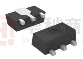
SOT-89
Applications
SOT-23
D
Quick Charge (QC4.0)/ Type C PD Charger or Adapter
Current Source
Voltage Source
D
D
S
G
G
D
G
S
S
General Description
DMZ0615E/ DMX0615E / DMZ0622E/ DMX0622E /DMX1015E- novel series of depletion mode
MOSFETs are designed with ARK Microelectronics proprietary and patent ultrahigh threshold voltage
technology. DMZ0622E is a wide range voltage (up to 70V) regulator. Its input voltage can be 70V high, and it
also can provide stable output voltage from about 11V to 23V in accordance with different work conditions. It is
very suitable for Quick Charge (QC4.0) / Type C PD Charger application which have variable charging voltage
output ( 5-20V).
By using the sub threshold characteristics, the depletion mode MOSFET DMZ0622E can provide stable
power to the load, and the voltage of load can be clamped to protect the load without zener diode.
DMZ0622E can endure wide voltage input up to 70V, and can provide with proper voltage to the load. These
characteristics are fit for the application of Quick Charge (QC4.0) /Type C PD Charger, and its PWM control IC
need to be powered with stable voltage.
Ordering Information
Part Number
Package
Marking
Remark
DMZ0622E
SOT-23
0622
Halogen Free
DMX0622E
SOT-89
0622
Halogen Free
Absolute Maximum Ratings
Symbol
Parameter
VDSX
Drain-to-Source Voltage
VDGX
ID
TA=25℃ unless otherwise specified
DMZ0622E
[1]
DMX0622E
Unit
70
V
Drain-to-Gate Voltage[1]
70
V
Continuous Drain Current
0.1
[2]
A
IDM
Pulsed Drain Current
PD
Power Dissipation
VGS
Gate-to-Source Voltage
±30
V
VESD(G-S)
Gate Source ESD
IEC, C=150pF, R=330Ω
400
V
Soldering Temperature
Distance of 1.6mm from case for 10 seconds
300
TL
TJ and TSTG
0.4
0.5
Operating and Storage Temperature Range
1.0
W
℃
-55 to 150
Caution: Stresses greater than those listed in the “Absolute Maximum Ratings” may cause permanent damage to the device.
ARK Microelectronics Co., Ltd.
www.ark-micro.com
1/8
Rev. 2.2 May. 2020
�DMZ0622E/ DMX0622E
Thermal Characteristics
Symbol
RθJA
Parameter
Thermal Resistance, Junction-to-Ambient
DMZ0622E
DMX0622E
Unit
250
125
K/W
Electrical Characteristics
OFF Characteristics
Symbol
BVDSX
Parameter
Drain-to-Source Breakdown Voltage
ID(OFF)
Drain-to-Source Leakage Current
IGSS
Gate-to-Source Leakage Current
TA =25℃ unless otherwise specified
Min.
70
Typ.
--
Max.
--
Unit
V
Test Conditions
VGS=-30V, ID=250µA
--
--
15
µA
VDS=70V,VGS= -30V
--
--
1.0
mA
---
---
20
-20
µA
ON Characteristics
Symbol
IDSS
Parameter
Saturated Drain-to-Source Current
RDS(ON)
Static Drain-to-Source On-Resistance
VGS(OFF)
Gate-to-Source Cut-off Voltage
gfs
Forward Transconductance
TA =25℃ unless otherwise specified
Min.
120
Typ.
--
Max.
--
Unit
mA
Test Conditions
VGS=0V, VDS=25V
--
10
15
Ω
VGS=0V,ID=100mA [3]
-19
-22
-25
V
VDS =20V, ID=8µA
--
130
--
mS
VDS =20V, ID=5mA
Dynamic Characteristics
Symbol
CISS
COSS
CRSS
QG
QGS
QGD
Parameter
Input Capacitance
Output Capacitance
Reverse Transfer Capacitance
Total Gate Charge
Gate-to-Source Charge
Gate-to-Drain (Miller) Charge
Essentially independent of operating temperature
Min.
-------
Typ.
1.5
2.6
0.74
9
1.5
2.3
Resistive Switching Characteristics
Symbol
td(ON)
trise
td(OFF)
tfall
Parameter
Turn-on Delay Time
Rise Time
Turn-off Delay Time
Fall Time
Parameter
Diode Forward Voltage
Max.
-------
Unit
Test Conditions
pF
VGS=-30V
VDS=25V
f=1.0MHZ
nC
VGS= -30V~0V
VDS=30V, ID=100mA
Essentially independent of operating temperature
Min.
-----
Typ.
17
200
11
4
Source-Drain Diode Characteristics
Symbol
VSD
VDS=70V,VGS= -30V
TJ=125℃
VGS=+30V, VDS=0V
VGS=-30V, VDS=0V
Max.
-----
Unit
Test Conditions
us
VGS = -30V~-0V
VDD = 35V, ID=100mA
RG = 20Ohm
TA=25℃ unless otherwise specified
Min
--
Typ.
--
Max.
1.2
Units
V
Test Conditions
ISD =100 mA, VGS = -30 V
NOTE:
[1] TJ=+25℃ to +150℃
[2] Repetitive rating, pulse width limited by maximum junction temperature.
[3] Pulse width≤380µs; duty cycle≤2%.
ARK Microelectronics Co., Ltd.
www.ark-micro.com
2/8
Rev. 2.2 May. 2020
�DMZ0622E/ DMX0622E
Typical and highlight Characteristics
0.12
0.10
0.8
ID, Drain Current (A)
PD, Power Dissipation (W)
1
Figure 2. Maximum Continuous Drain
Current vs Case Temperature
Figure 1. Maximum Power Dissipation vs.
Case Temperature
SOT-89
0.6
0.4
SOT-23
0.2
0.08
0.06
0.04
0.02
0.00
0
25
50
75
100
125
25
150
50
TC, Case Temperature (℃)
75
100
125
TC, Case Temperature (℃)
150
DMZ0622E/DMX0622E can be used as a current or voltage source to supply power to the load, as shown in
Figure 3.
Figure 3.
DMZ0622E/DMX0622E as a voltage source
The output voltage Vout is determined by the load RL, current ID and VGS(OFF) :.
ID = IDSS(1+IDRL/VGS(OFF))2
Vout = -VGS = IDRL
1.E-02
20
ID
Vout
1.E-03
16
1.E-04
12
1.E-05
1.E-06
1E+02
Vout, Output Voltage(V)
ID, Drain Current(A)
Figure 4. DMZ0622E/DMX0622E output Characteristics vs. Load Resistance
1.E-01
24
8
1E+03
ARK Microelectronics Co., Ltd.
1E+04
1E+05
1E+06
RL, Load Resistance(ohm)
www.ark-micro.com
3/8
1E+07
Rev. 2.2 May. 2020
�DMZ0622E/ DMX0622E
From the above function, we can see the depletion mode MOSFET operate in sub-threshold region, the Vout
is always below or closed to the threshold voltage or Gate-to-Source Cut-off Voltage VGS(OFF), no matter how the
input voltage Vin changes. Therefore, in addition to provide power for load like IC, the output voltage Vout can be
clamped to the VGS(OFF), the IC is then protected from variable voltage or current. DMZ0622E/DMX0622E can
support up to 70V input voltage. Vout and Vin have relations following the formulas:
If
Vin <∣VGS(OFF)∣, then
If
Vin ≥∣VGS(OFF)∣, then
Vout ≈ Vin
Vout ≤ VGS(OFF)
The Ultrahigh Threshold Voltage Depletion Mode Power MOSFET--DMZ0622E/DMX0622E, was
developed by ARK Microelectronics proprietary and patent technology. The threshold voltage VGS(OFF) of
DMZ0622E/DMX0622E is between -19V and -25V, can provide sufficient voltage for load such like a PWM IC
in the primary side of a Flyback converter.
Since DMZ0622E/DMX0622E has a variation distribution of VGS(OFF), from -19V to -25V, so its output
voltage is different with different VGS(OFF). Figure 5 shows the characteristics of output voltage Vout vs. junction
temperature of two DMZ0622E/DMX0622E MOSFETS which has the highest VGS(OFF),=-19V and lowest
VGS(OFF),=-25V respectively. This means the clamped voltage of Vout will also change with temperature and
VGS(OFF).
Figure 5. Output voltage vs. Junction Trmperature
Vout, Output voltage(V)
28
Load Current=8uA
26
VGS(OFF)=-25V
24
22
20
VGS(OFF)=-19V
18
-10
10
30
50
70
90
110
TJ, Junction Temperature(℃)
130
150
Fig 6 and Fig 7 shows the characteristics of output voltage Vout vs. load current IRL and junction temperature
TJ of two DMZ0622E/DMX0622E MOSFETS which has the highest VGS(OFF),=-19V and lowest VGS(OFF),=-25V
respectively.
Figure 6. Output Voltage vs. Load
Current
26
Figure 7. Output Voltage vs. Load
Current
26
VGS(OFF)=-19V
Vout, Output voltage(V)
VGS(OFF)=-25V
Vout, Output voltage(V)
22
TJ=150℃
18
TJ=25℃
14
24
22
TJ=150℃
20
TJ=25℃
18
TJ=-10℃
TJ=-10℃
16
10
0
2
4
6
ID, Drain Current(mA)
ARK Microelectronics Co., Ltd.
8
10
0
2
www.ark-micro.com
4/8
4
6
8
ID, Drain Current(mA)
10
Rev. 2.2 May. 2020
�DMZ0622E/ DMX0622E
Typical applications:
Figure 8 is a typical schematic of a primary side of a Flyback power source, it serves as a quick charger with
TypeC PD or Quick Charge( QC) protocols. These kind of quick chargers can provide variable charging voltage
(from 5-20V) output, these voltages will turn back to the primary side, so that the voltage of auxilary coil, which
is used as a power source to PWM IC has to be changed in a wide ranges, even it can be too high to use for PWM
IC. The normal solution is using a transistor and zener diode and some resistors to provide PWM IC with stable
voltage. But the circuit is complicated and the BOM cost is higher.
The alternate cost effective solution is represent in Figure 9. The transistor, zener diode and resistors in Figure 8
can be simply replaced with DMZ0622E/DMX0622E, then the space of PCB is saved with fewer components,
and the cost will be down.
The depletion mode MOSFET DMZ6005E is used for start-up, when the charger start to work, the auxilary coil
will supply voltage for the PWM IC, then DMZ6005E is shut off, so that the standby power dispation of system
will be significantly low. The documents of DMZ6005E can be accessed in ARK’s website.
Figure 8. Normal circuit with transistor and diode
Figure 9. Circuit with DMZ0622E/DMX0622E
ARK Microelectronics Co., Ltd.
www.ark-micro.com
5/8
Rev. 2.2 May. 2020
�DMZ0622E/ DMX0622E
Package Dimensions
ARK Microelectronics Co., Ltd.
www.ark-micro.com
6/8
Rev. 2.2 May. 2020
�DMZ0622E/ DMX0622E
ARK Microelectronics Co., Ltd.
www.ark-micro.com
7/8
Rev. 2.2 May. 2020
�DMZ0622E/ DMX0622E
Published by
ARK Microelectronics Co., Ltd.
ADD: 4F, D26, UESTC National Science Park No. 1 Shuangxing Avenue, Gongxing Street,
Shuangliu District, Chengdu, China (Sichuan) Pilot Free Trade Zone.
Tel:+86-28-8523-2215
Email: sales@ark-micro.com http://www.ark-micro.com
All Rights Reserved
Disclaimers
ARK Microelectronics Co., Ltd. reserves the right to make change without notice in order to improve
reliability, function or design and to discontinue any product or service without notice. Customers should obtain
the latest relevant information before orders and should verify that such information is current and complete. All
products are sold subject to ARK Microelectronics Co., Ltd.’s terms and conditions supplied at the time of
order acknowledgement.
ARK Microelectronics Co., Ltd. warrants performance of its hardware products to the specifications at the
time of sale, Testing, reliability and quality control are used to the extent ARK Microelectronics Co., Ltd
deems necessary to support this warrantee. Except where agreed upon by contractual agreement, testing of all
parameters of each product is not necessary performed.
ARK Microelectronics Co., Ltd. does not assume any liability arising from the use of any product or circuit
designs described herein. Customers are responsible for their products and applications using ARK
Microelectronics Co., Ltd.’s components. To minimize risk, customers must provide adequate design and
operating safeguards.
ARK Microelectronics Co., Ltd. does not warrant or convey any license either expressed or implied under its
patent rights, nor the rights of others. Reproduction of information in ARK Microelectronics Co., Ltd.’s data
sheets or data books is permissible only if reproduction is without modification or alteration. Reproduction of this
information with any alteration is an unfair and deceptive business practice. ARK Microelectronics Co., Ltd is
not responsible or liable for such altered documentation.
Resale of ARK Microelectronics Co., Ltd.’s products with statements different from or beyond the parameters
stated by ARK Microelectronics Co., Ltd. for the product or service voids all express or implied warrantees for
the associated ARK Microelectronics Co., Ltd.’s product or service and is unfair and deceptive business
practice. ARK Microelectronics Co., Ltd is not responsible or liable for any such statements.
Life Support Policy:
ARK Microelectronics Co., Ltd.’s products are not authorized for use as critical components in life devices or
systems without the expressed written approval of ARK Microelectronics Co., Ltd.
As used herein:
1. Life support devices or systems are devices or systems which:
a. are intended for surgical implant into the human body,
b. support or sustain life,
c. whose failure to perform when properly used in accordance with instructions for used provided in the
labeling, can be reasonably expected to result in significant injury to the user.
2. A critical component is any component is any component of a life support device or system whose failure
to perform can be reasonably expected to cause the failure of the life support device or system, or to affect
its safety or effectiveness.
ARK Microelectronics Co., Ltd.
www.ark-micro.com
8/8
Rev. 2.2 May. 2020
�