NSi1312
High Reliability Reinforced
Isolated Amplifier
Datasheet (EN) 1.2
Key Features
Up to 5000VRMS Insulation Voltage
±1.2V Linear Input Voltage Range
Offset Drift: ±20μV/℃ (Typ)
Gain Error: ±1% (Max)
Gain Drift: ±30ppm/℃ (Typ)
Nonlinearity: ±0.3% (Max)
Nonlinearity Drift: ±10ppm/℃ (Typ)
SNR: 72dB (Typ)
SOP8 narrow body (SOP 150mil)
UL recognition:
SOW8: 5000Vrms for 1 minute per UL1577
SOP8: 3000Vrms for 1 minute per UL1577
CQC certification per GB4943.1-2011
CSA component notice 5A approval IEC60950-1 standard
DIN VDE V 0884-11:2017-01
Applications
AC motor controls
Power and solar inverters
Uninterruptible Power Suppliers
Automotive onboard chargers
Device Information
Part Number
NSI1312x-DSWVR
Package
SOW8(300mil)
Body Size
5.85mm × 7.50mm
NSI1312x-DSPR
SOP8(150mil)
4.90mm × 3.90mm
Functional Block Diagrams
VDD1
Excellent DC Performance:
Offset Error: ±5mV (Max)
SOW8 wide body (SOP8 300mil)
Safety Regulatory Approvals
Fixed Gain : 1
VDD2
VDD1 detection
Reference
INP
Σ-Δ modulator
INN
Copyright © 2022, NOVOSENSE
Retiming
and 4thOrder Active
Low-Pass
Filter
OUTP
OUTN
Reference
GND1
GND2
Figure 1. NSi1312D Block Diagram
VDD1
VDD2
VDD1 detection
Reference
INP
Σ-Δ modulator
INN
TX
RX
Oscillator
VDD1 monitoring
Operation Temperature: -40℃~125℃
RX
Oscillator
High CMTI: 100kV/μs (Typ)
System-Level Diagnostic Features:
TX
Isolation Barrier
NSI1312 is a cost-effective isolated amplifier with output
separated from input based on the NOVOSENSE capacitive
isolation technology Adaptive OOK®. The device has a
linear differential input signal range of ±1.2V (±1.5V fullscale). The high input impedance of NSI1312 makes it
highly suitable for connection to high-voltage resistive
dividers or other voltage signal sources with high output
resistance.
The device has a fixed gain of 1 and provides differential
analog output version(NSI1312D) and single-ended
analog output version(NSI1312S) option.
The low offset and gain drift ensure the accuracy over the
entire temperature range. The high common-mode
transient immunity ensures that the device is able to
provide accurate and reliable measurements even in the
presence of high-power switching such as in motor
control applications.
The fail-safe function (missing VDD1 detection) simplifies
system-level design and diagnostics.
RoHS-Compliant Packages:
Isolation Barrier
Product Overview
GND1
Retiming
and 4thOrder Active
Low-Pass
Filter
OUT
Reference
REFIN
GND2
Figure 2. NSi1312S Block Diagram
Page 1
�NSi1312
Datasheet (EN) 1.2
INDEX
1. PIN CONFIGURATION AND FUNCTIONS............................................................................................................................. 3
2. ABSOLUTE MAXIMUM RATINGS ......................................................................................................................................... 5
3. RECOMMENDED OPERATING CONDITIONS ....................................................................................................................... 5
4. THERMAL INFORMATION ................................................................................................................................................... 5
5. SPECIFICATIONS ................................................................................................................................................................ 5
5.1.
5.2.
5.3.
5.4.
ELECTRICAL CHARACTERISTICS....................................................................................................................................... 6
POWER RATING CHARACTERISTICS .................................................................................................................................. 7
TYPICAL PERFORMANCE CHARACTERISTICS ...................................................................................................................... 8
PARAMETER MEASUREMENT INFORMATION .................................................................................................................... 10
6. HIGH VOLTAGE FEATURE DESCRIPTION .......................................................................................................................... 11
6.1.
6.2.
6.3.
INSULATION AND SAFETY RELATED SPECIFICATIONS ......................................................................................................... 11
INSULATION CHARACTERISTICS..................................................................................................................................... 11
REGULATORY INFORMATION ......................................................................................................................................... 13
7. FUNCTION DESCRIPTION ................................................................................................................................................ 13
7.1.
7.2.
7.3.
OVERVIEW ................................................................................................................................................................ 13
ANALOG INPUT .......................................................................................................................................................... 14
ANALOG OUTPUT ....................................................................................................................................................... 14
8. APPLICATION NOTE ......................................................................................................................................................... 17
8.1.
8.2.
8.3.
TYPICAL APPLICATION CIRCUIT .................................................................................................................................... 17
SENSE RESISTOR SELECTION ....................................................................................................................................... 17
PCB LAYOUT ............................................................................................................................................................ 18
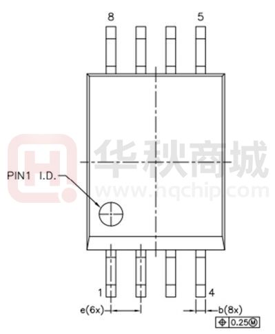
9. PACKAGE INFORMATION ................................................................................................................................................. 18
10. ORDERING INFORMATION ............................................................................................................................................. 21
11. DOCUMENTATION SUPPORT ......................................................................................................................................... 21
12. TAPE AND REEL INFORMATION ..................................................................................................................................... 22
13. REVISION HISTORY ........................................................................................................................................................ 24
Copyright © 2022, NOVOSENSE
Page 2
�NSi1312
Datasheet (EN) 1.2
1. Pin Configuration and Functions
VDD1
1
INP
2
INN
3
GND1
4
NSI1312D
TOP VIEW
8
VDD2
7
OUTP
6
OUTN
5
GND2
Figure 1.1 NSi1312D Package (SOW8 and SOP8)
Table 1.1 NSi1312D Pin Configuration and Description
NSi1312D PIN
NO.
SYMBOL
FUNCTION
1
VDD1
Power supply for isolator input side (4.5V to 5.5V)
2
INP
Positive analog input
3
INN
Negative analog input
4
GND1
Ground 1, the ground reference for input side
5
GND2
Ground 2, the ground reference for output side
6
OUTN
Negative output
7
OUTP
Positive output
8
VDD2
Power supply for isolator output side (3.0V to 5.5V)
Copyright © 2022, NOVOSENSE
Page 3
�NSi1312
Datasheet (EN) 1.2
VDD1
1
INP
2
INN
3
GND1
4
NSI1312S
TOP VIEW
8
VDD2
7
OUT
6
REFIN
5
GND2
Figure 1.2 NSi1312S Package (SOW8 and SOP8)
Table 1.2 NSi1312S Pin Configuration and Description
NSi1312S PIN
NO.
SYMBOL
FUNCTION
1
VDD1
Power supply for input side (4.5V to 5.5V)
2
INP
Positive analog input
3
INN
Negative analog input
4
GND1
Ground 1, the ground reference for input side
5
GND2
Ground 2, the ground reference for output side
6
REFIN
External Reference Input
7
OUT
Output
8
VDD2
Power supply for output side (3.0V to 5.5V)
Copyright © 2022, NOVOSENSE
Page 4
�NSi1312
Datasheet (EN) 1.2
2. Absolute Maximum Ratings
Parameters
Symbol
Min
VDD1, VDD2
-0.3
6.5
V
INP, INN
GND1-6
VDD1+0.5
V
REFIN
GND2-0.5
VDD2+0.5
V
OUTP, OUTN,
OUT
GND2-0.5
VDD2+0.5
V
Io
-10
10
mA
Operating Temperature
TOPR
-40
125
℃
Junction Temperature
TJ
-40
150
℃
Storage Temperature
TSTG
-55
150
℃
HBM (1)
±2000
V
CDM (2)
±1000
V
Power Supply Voltage
Input Voltage
Output Voltage
Output current per Output Pin
Electrostatic discharge
Typ
Max
Unit
(1) Human body model (HBM), per AEC-Q100-002-RevD
(2) Charged device model (CDM), per AEC-Q100-011-RevB
3. Recommended Operating Conditions
Parameters
Symbol
Min
Typ
Max
Unit
Input side Power Supply
VDD1
3.0
5.0
5.5
V
Output side Power Supply
VDD2
3.0
3.3
5.5
V
Differential input voltage before clipping
output
VClipping
Linear differential input full scale voltage
VFSR
-1.2
1.2
V
Operating common-mode input voltage
VCM
-0.8
0.8
V
Operating Ambient Temperature
TA
-40
125
℃
±1.5
V
4. Thermal Information
Parameters
Symbol
SOW8
SOP8
Unit
Junction–to-ambient thermal resistance
RθJA
86
137.7
℃/W
Junction-to-case (top) thermal resistance
RθJC(top)
28
54.9
℃/W
Junction-to-board thermal resistance
RθJB
42
71.7
℃/W
Junction–to-top characterization parameter
ΨJT
4
12
℃/W
Junction-to-board characterization parameter
ΨJB
42
46
℃/W
5. Specifications
Copyright © 2022, NOVOSENSE
Page 5
�NSi1312
Datasheet (EN) 1.2
5.1. Electrical Characteristics
(AVDD = 3.0V ~ 5.5V, DVDD = 3.0V ~ 5.5V, INP = -1.2V to +1.2V, and INN = AGND = 0V, TA = -40℃ to 125℃. Unless otherwise noted,
Typical values are at VDD1 = 5V, VDD2 = 3.3V, TA = 25℃.Output characteristics is based on OUTP-OUTN for NSI1312D, is based on
OUT-REFIN for NSI1312S.)
Parameters
Symbol
Min
Typ
Max
Unit
Input side supply voltage
VDD1
3.0
5.0
5.5
V
Output side supply voltage
VDD2
3.0
5.0
5.5
V
Input side supply current
IDD1
7.2
9
mA
Output side supply current
IDD2
4.7
6.2
mA
Comments
Power Supply
VDD1 undervoltage detection
threshold voltage
VDD1UV
1.8
2.3
2.7
V
VOS
-5
±1
5
mV
TCVOS
-25
0.5
25
μV/°C
VDD1 falling
Analog Input
Input offset voltage
Input offset drift
INP = INN = GND1, at TA =25℃
CMRRdc
-80
dB
INP = INN, fIN = 0 Hz, VCM min ≤ VIN ≤
VCM max
CMRRac
-82
dB
INP = INN, fIN = 10 kHz, VCM min ≤ VIN
≤ VCM max
Single-ended input resistance
RIN
1
MΩ
INN = GND1
Differential input resistance
RIND
1.6
MΩ
Input capacitance
CI
2
pF
Input bias current
IIB
Common-mode rejection ratio
Input bias current drift
-0.7
TCIIB
-0.6
-0.5
uA
-1
nA/°C
1
V/V
INP = INN = GND1, at TA =25℃, IIB =
(IIBP + IIBN) / 2
Analog Output
Nominal Gain
Gain error
Gain error thermal drift
EG
-0.4%
±0.1%
0.4%
TCEG
-50
-10
50
-0.05%
±0.01%
0.05%
Nonlinearity
Nonlinearity drift
Total harmonic distortion
THD
Output noise
Signal to noise ratio
SNR
Common-mode output voltage
VCMout
Copyright © 2022, NOVOSENSE
1.39
at TA =25℃
ppm/°C
at TA =25℃
±1
ppm/°C
-70
dB
100
µVRMS
78
dB
1.44
1.49
V
VIN =±1.2V, fIN = 10kHz, BW = 50kHz
INP = INN = GND1, BW = 50kHz
VIN =±1.2V, fIN = 10kHz, BW = 50kHz
Only for NSI1312D
Page 6
�NSi1312
Differential fail-safe output
voltage
Datasheet (EN) 1.2
VFAILSAFE
-1.8
-1.7
0
Single-ended fail-safe output
voltage
VFAILSAFE
Single end reference input
REFIN
Single end reference input
impedance
REFININ
V
NSI1312D VDD1 missing
V
NSI1312S VDD1 missing,
REFIN1.8V
VDD21.5
V
Only for NSI1312S. See
application description for more
details.
1
GΩ
100
kHz
PSRRdc
-95
dB
PSRR vs VDD1, at DC
PSRRac
-95
dB
PSRR vs VDD1, 100mV and 10kHz
ripple
PSRRdc
-90
dB
PSRR vs VDD2, at DC
PSRRac
-80
dB
PSRR vs VDD2 for NSI1312D,
100mV and 10kHz ripple
PSRRac
-72
dB
PSRR vs VDD2 for NSI1312S,
100mV and 1kHz ripple
Output resistance
ROUT
< 0.2
Ω
Output limit current
ILIM
±13
mA
150
kV/μs
Output bandwidth
Power supply rejection ratio
Common-mode transient
immunity
BW
CMTI
50
100
Only for NSI1312S
Common-mode transient
immunity
Timing
Rising time of OUTP, OUTN
tr
3.6
μs
Falling time of OUTP, OUTN
tf
3.6
μs
INP, INN to OUTP, OUTN signal
delay (50% - 50%)
tPD
3.5
Analog setting time
tAS
0.5
4
μs
ms
VDD1 step to 5.0 V with VDD2 ≥ 3.0
V, to OUTP, OUTN valid, 0.1%
settling
5.2. Power Rating Characteristics
Parameters
Symbol
Max
Unit
Comments
Total Power dissipation
PD
83.6
mW
VDD1=VDD2=5.5V
Power dissipation of high side
PD1
49.5
mW
VDD1=5.5V
Power dissipation of low side
PD2
34.1
mW
VDD2=5.5V
Copyright © 2022, NOVOSENSE
Page 7
�NSi1312
Datasheet (EN) 1.2
5.3. Typical Performance Characteristics
Unless otherwise noted, test at NSI1312D VDD1 = 5V, VDD2 = 3.3V, INN=GND1=0V, INP = -1.2V to 1.2V, fIN = 1kHz, BW = 10kHz.
Characteristics of NSI1312S may be related to REFIN accuracy.
0.4
0.02
0.3
0.018
Sample1
0.016
Sample2
0.014
Sample3
Nonlinearity/%
0.2
Vos/mV
0.1
0
-0.1
Sample 1
-0.2
-40
-20
0
20
40
60
80
100
0.006
0.002
Sample 3
-0.4
0.01
0.008
0.004
Sample 2
-0.3
0.012
0
120
-40
140
-20
0
20
Templerature(℃)
60
80
100
120
140
Figure 5. 3 Nonlinearity vs Temperature
Figure 5. 1 Input Offset Voltage vs Temperature
-0.55
0.2
0.15
Sample 1
0.1
Sample 2
0.05
Sample 3
Sample 1
-0.56
Sample 2
Sample 3
-0.57
IIByuA
Gain Error/%
40
Templerature(℃)
0
-0.05
-0.58
-0.59
-0.1
-0.6
-0.15
-0.61
-0.2
-40
-20
0
20
40
60
80
100
120
-40
140
-20
0
20
40
60
80
100
120
140
Templerature(℃)
Templerature(℃)
Figure 5. 4 Input Bias Current vs Temperature
Figure 5. 2 Gain Error vs Temperature
-60
1.6
-65
1.59
-75
RinDyMΩ
CMRRydB
-70
-80
1.58
1.57
-85
1.56
-90
-95
-40
-20
0
20
40
60
80
100
120
140
Templerature(℃)
Figure 5. 5 Common-Mode Rejection Ratio vs Temperature
Copyright © 2022, NOVOSENSE
1.55
-40
-20
0
20
40
60
80
100
120
140
Templerature(℃)
Figure 5. 6 Differential Input Resistance vs Temperature
Page 8
�Datasheet (EN) 1.2
-65
-65
-66
-66
-67
-67
-68
-68
-69
-69
THDydB
THDydB
NSi1312
-70
-71
-72
VDD1
VDD2
-70
-71
-72
-73
-73
-74
-74
-75
-40
-20
0
20
40
60
80
100
120
-75
140
3
Templerature(℃)
4.5
5
5.5
Figure 5. 8 THD vs Supply Voltage
82
82
81
81
80
80
79
SNRydB
SNRydB
4
Supply Voltage(V)
Figure 5. 7 THD vs Temperature
78
77
VDD1
VDD2
79
78
77
76
76
75
-40
-20
0
20
40
60
80
100
120
75
140
3
Templerature(℃)
3.5
4
4.5
5
5.5
Supply Voltage(V)
Figure 5. 9 SNR vs Temperature
Figure 5. 10 SNR vs Supply Voltage
0
2.5
vs VDD1
-20
2
vs VDD2
Output VoltageyV
-40
PSRRydB
3.5
-60
-80
1.5
1
0.5
-100
-120
0.1
1
10
100
Frequency(kHz)
Figure 5. 11 Power-Supply Rejection Ratio vs Ripple
Frequency (NSI1312D)
Copyright © 2022, NOVOSENSE
1000
OUTP-GND
OUTN-GND
0
-2
-1.5
-1
-0.5
0
0.5
1
1.5
2
Input Voltage(V)
Figure 5. 12 Output Voltage vs Input Voltage (NSI1312D)
Page 9
�NSi1312
Datasheet (EN) 1.2
-1.75
1.5
Common Mode VoltageyV
Failsafe VoltageyV
-1.76
-1.77
-1.78
-1.79
-1.8
-1.81
1.48
1.46
1.44
1.42
-1.82
1.4
-40
-20
0
20
40
60
80
100
120
140
-40
-20
0
20
40
Templerature(℃)
Figure 5. 13 Fail-Safe Output Voltage vs
Temperature(NSI1312D)
3.5
100
120
140
8
7.5
3.49
3.485
Supply CurrentymA
Propagation Delayyus
80
Figure 5. 14 Output Common-Mode Voltage vs
Temperature(NSI1312D)
3.495
3.48
3.475
3.47
3.465
7
6.5
3.46
3.455
4.5
-20
0
20
40
60
80
100
120
VDD2=3.3V
5.5
5
-40
VDD1=5V
6
3.45
4
140
-1.2
-0.7
-0.2
Templerature(℃)
0.3
0.8
Input Voltage(V)
Figure 5. 15 Vin to Vout Delay vs Temperature
Figure 5. 16 Supply Current vs Input Voltage
8
7.5
7.5
7
7
6.5
VDD1=5V
6
VDD2=3.3V
5.5
5
4.5
Supply CurrentymA
Supply CurrentymA
60
Templerature(℃)
6.5
6
VDD1
5.5
VDD2
5
4.5
4
-40
-20
0
20
40
60
80
100
120
140
Temperature(C)
Figure 5. 17 Supply Current vs Temperature
4
3
3.5
4
4.5
5
5.5
Supply Voltage(V)
Figure 5. 18 Supply Current vs Supply Voltage
5.4. Parameter Measurement Information
Copyright © 2022, NOVOSENSE
Page 10
�NSi1312
Datasheet (EN) 1.2
3.3V
Battery
VDD1
VDD2
INP
OUTP
INN
OUTN
GND1
GND2
Differential
Probe
Oscilloscope
High Voltage
Probe
VCM
Figure 5.19 Common-Mode Transient Immunity Test Circuit
6. High Voltage Feature Description
6.1. Insulation and Safety Related Specifications
Parameters
Symbol
Value
Unit
Comments
SOW8
SOP8
CLR
8
4
mm
Shortest terminal-to-terminal
distance through air
Minimum External Tracking
(Creepage)
CPG
8
4
mm
Shortest terminal-to-terminal
distance across the package
surface
Minimum internal gap
DTI
28
μm
Distance through insulation
Tracking Resistance
(Comparative Tracking Index)
CTI
>600
V
Minimum External Air Gap
(Clearance)
Material Group
I
DIN EN 60112 (VDE 0303-11); IEC
60112
IEC 60664-1
6.2. Insulation Characteristics
Description
Test Condition
Symbol
Value
Unit
DIN VDE 0110
SOP8
SOW8
For Rated Mains Voltage ≤ 150Vrms
I to IV
I to IV
For Rated Mains Voltage ≤ 300Vrms
I to III
I to IV
For Rated Mains Voltage ≤ 600Vrms
I to II
I to IV
40/125/21
40/125/21
2
2
990
2121
VPEAK
700
1500
VRMS
990
2121
VDC
Climatic Classification
Pollution Degree per DIN VDE 0110,
Table 1
Maximum repetitive isolation voltage
Maximum working isolation voltage
Copyright © 2022, NOVOSENSE
VIORM
AC Voltage
DC Voltage
VIOWM
Page 11
�NSi1312
Datasheet (EN) 1.2
Description
Test Condition
VIORM × 1.5 = Vpd (m), 100%
production test,
Input to Output Test Voltage, Method B1
Input to Output Test Voltage, Method A. After
Input and /or Safety Test Subgroup 2 and
Subgroup 3
Maximum transient isolation voltage
Maximum Surge Isolation Voltage
Isolation resistance
Isolation capacitance
Safety total power dissipation
Safety input, output, or supply current
Value
Unit
V pd (m)
1485
/
VPEAK
V pd (m)
/
3977
VPEAK
VIORM × 1.3 = Vpd (m), tini = 60 sec,
tm = 10 sec, partial discharge
< 5 pC
V pd (m)
1287
/
VPEAK
VIORM × 1.6 = Vpd (m), tini = 60 sec,
tm = 10 sec, partial discharge
< 5 pC
V pd (m)
/
3394
VPEAK
VIORM × 1.2= Vpd (m), tini = 60 sec,
tm = 10 sec, partial discharge
< 5 pC
V pd (m)
1188
2545
VPEAK
t = 60 sec
VIOTM
4242
7000
VPEAK
Test method per
IEC62368-1, 1.2/50us
waveform, VTEST=VIOSM×1.3
VIOSM
6000
/
VPEAK
Test method per
IEC62368-1, 1.2/50us
waveform, VTEST=VIOSM×1.6
VIOSM
/
6250
VPEAK
VIO =500V, Tamb=Ts
RIO
>109
>109
Ω
VIO =500V, 100℃ ≤ Tamb ≤
125℃
RIO
>1011
>1011
Ω
f = 1MHz
CIO
0.8
0.8
pF
VI = 5.5V, TJ = 150 ℃, TA =
25 ℃
Ps
907
1453
mW
165
/
mA
/
264
mA
Ts
150
150
℃
VISO
3000
5000
VRMS
tini = tm = 1 sec, partial
discharge < 5 pC
VIORM × 1.875 = Vpd (m), 100%
production test,
tini = tm = 1 sec, partial
discharge < 5 pC
Input to Output Test Voltage, Method A.
After Environmental Tests Subgroup 1
Symbol
θJA = 137.7℃/W for SOP8, VI =
5.5V, TJ = 150 ℃, TA = 25 ℃
θJA = 86℃/W for SOW8, VI =
5.5V, TJ = 150 ℃, TA = 25 ℃
Maximum safety temperature
Is
UL1577
Insulation voltage per UL
Copyright © 2022, NOVOSENSE
VTEST = VISO, t = 60 s
(qualification),
VTEST = 1.2 × VISO, t = 1 s (100%
production test)
Page 12
�NSi1312
Datasheet (EN) 1.2
Safety Limiting
Current(mA)
300
SOW8
250
SOP8
200
150
100
50
0
0
50
100
150
Ambient Temperature(℃)
200
Figure 6.1 NSi1312x Thermal Derating Curve, Dependence of Safety Limiting Values with Case Temperature per DIN VDE V 0884-11
6.3. Regulatory Information
The NSi1312x-DSWVR are approved or pending approval by the organizations listed in table.
UL
VDE
CQC
Certified by CQC11-4715432012
UL 1577 Component
Recognition Program
Approved under CSA
Component Acceptance
Notice 5A
DIN VDE V 0884-11(VDE V
0884-11):2017-01
Single Protection, 5000Vrms
Isolation voltage
Single Protection, 5000Vrms
Isolation voltage
Reinforce Insulation
2121Vpeak, VIOSM=6250Vpeak
Reinforced insulation
Certificate No.E500602
Certificate No.E500602
File (pending)
CQC20001264940
GB4943.1-2011
The NSi1312x-DSPR are approved or pending approval by the organizations listed in table.
UL
VDE
CQC
Certified by CQC11-4715432012
UL 1577 Component
Recognition Program
Approved under CSA
Component Acceptance
Notice 5A
DIN VDE V 0884-11(VDE V
0884-11):2017-01
Single Protection, 3000Vrms
Isolation voltage
Single Protection, 3000Vrms
Isolation voltage
Basic Insulation 990Vpeak,
VIOSM=6000Vpeak
Basic insulation
Certificate No.E500602
Certificate No.E500602
File (pending)
CQC20001264940
GB4943.1-2011
7. Function Description
7.1. Overview
The NSI1312 is a cost-effective isolated amplifier with a high input impedance that accept wide range fully-differential input. The
fully-differential input is suited to AC or bus voltage monitoring in high voltage applications where isolation is required. The analog
input is continuously sampled by a second-order Σ-Δ modulator in the device. With the internal voltage reference and clock
generator, the modulator converts the analog input signal to a digital bitstream, as shown in the Figure 7.1. The output of the
modulator is transferred by the drivers (called TX in the Functional Block Diagram) across the isolation barrier that separates the
isolated input side and output side voltage. The received bitstream and clock are synchronized and processed, as shown in the
Functional Block Diagram, by a fourth-order analog filter on the output side and has a differential output. NSI1312 also has singleended output version, as shown in the Figure 7.2, the received bitstream are processed and presented as a single-ended output with
external voltage reference from REFIN pin.
Copyright © 2022, NOVOSENSE
Page 13
�NSi1312
Datasheet (EN) 1.2
VDD1
VDD2
VDD1 detection
INP
Σ-Δ modulator
TX
INN
Isolation Barrier
Reference
Retiming
and 4thOrder Active
Low-Pass
Filter
RX
OUTP
OUTN
Reference
Oscillator
GND1
GND2
Figure 7.1 Function Block Diagram of Differential Output Version
VDD1
VDD2
VDD1 detection
INP
Σ-Δ modulator
INN
Oscillator
GND1
TX
Isolation Barrier
Reference
RX
Retiming
and 4thOrder Active
Low-Pass
Filter
OUT
Reference
REFIN
GND2
Figure 7.2 Function Block Diagram of Single-ended Output Version
7.2. Analog Input
There are two restrictions on the analog input signals (VINP and VINN).
If the input voltage exceeds the range AGND – 6 V to AVDD + 0.5 V, the input current must be limited to 10 mA because the device
input electrostatic discharge (ESD) diodes turn on.
The linearity and noise performance of the device are ensured only when the analog input voltage remains within the specified
linear full-scale range (FSR) and within the specified common-mode input voltage range.
7.3. Analog Output
For linear input range, the analog output of NSI1312 has a fixed gain of 1. If a full-scale input signal is applied to the NSI1312 (VIN ≥
VClipping), the differential analog output (VOUTP -VOUTN for NSI1312D and VOUT -REFIN for NSI1312S) will be clipped (typically, 1.44V for
positive clipping and -1.44V for negative clipping). The negative clipping differential output waveform is shown in Figure 7.3.
Copyright © 2022, NOVOSENSE
Page 14
�NSi1312
Datasheet (EN) 1.2
Vout 1V/div
Vneg_clip=-1.44V
Figure 7.3 Typical negative clipping output
For differential output version (NSI1312D), the differential output pins have a common-mode voltage of 1.44V (typ). The
differential output Vout of the NSI1312D is expressed as:
𝑉𝑜𝑢𝑡 = 𝐺𝑎𝑖𝑛 ∗ (𝑉
−𝑉
)
For single-ended output version (NSI1312S), the REFIN pin with high input impedance needs external reference input. The output
voltage Vout of the NSI1312S is expressed as:
𝑉𝑜𝑢𝑡 = 𝐺𝑎𝑖𝑛 ∗ (𝑉
−𝑉
) + 𝑅𝐸𝐹𝐼𝑁
In addition, NSI1312 integrates some diagnostic measures and offers a fail-safe output to simplify system-level design. The failsafe output is a negative differential output voltage that does not occur under normal device operation, and it will only be
activated when the undervoltage of VDD1 is detected (VDD1< VDD1UV). For NSI1312D, the typical failsafe output is -1.8V when VDD1
undervoltage, as is shown in Figure 7.4. For NSI1312S, the typical failsafe output is Vfailsafe= 0V if VREF