NSi826x
High Reliability Reinforced
Six-Channel Digital Isolators
Datasheet (EN) 1.6
Product Overview
The NSi826x devices are high reliability six-channel
digital isolators. The NSi826x device is safety certified
by UL1577 support several insulation withstand
voltage(3kV,3.75kV,5kV), while providing high
electromagnetic immunity and low emissions at low
power consumption. The data rate of the NSi826x is
up to 150Mbps, and the common-mode transient
immunity (CMTI) is up to 200kV/us. The NSi826x
device provides digital channel direction configuration
and the default output level configuration when the
input power is lost. Wide supply voltage of the
NSi826x device supports to connect with most digital
interface directly, easy to do the level shift. High
system level EMC performance enhance reliability
and stability of use.
Key Features
Up to 5000Vrms Insulation voltage
Safety Regulatory Approvals
UL recognition: up to 5000Vrms for 1 minute per
UL1577
CQC certification per GB4943.1-2011
CSA component notice 5A
DIN VDE V 0884-11:2017-01
Applications
Industrial automation system
Isolated SPI, RS232, RS485
General-purpose multichannel isolation
Device Information
Date rate: DC to 150Mbps
Part Number
NSi826x-DSWR
Power supply voltage: 2.5V to 5.5V
High CMTI: 200kV/us
Chip level ESD: HBM: ±8kV
High system level EMC performance:
Body Size
10.30mm × 7.50mm
NSi826x-DSSR
Package
SOP16(300mil)
SSOP16
NSi826x-DSPNR
SOP16(150mil)
9.90mm x 3.90mm
4.90mm × 3.90mm
Functional Block Diagrams
Enhanced system level ESD, EFT, Surge
immunity
Default output high level or low level option
Low power consumption: 1.5mA/ch (1 Mbps)
Low propagation delay: 600
Comparative Tracking Index
DIN EN 60112 (VDE 0303-11)
Material Group
IEC 60112
um
V
I
Installation Classification per DIN VDE 0110
For Rated Mains Voltage ≤ 150Vrms
I to III
I to IV
I to IV
For Rated Mains Voltage ≤ 300Vrms
I to II
I to IV
I to III
For Rated Mains Voltage ≤ 600Vrms
I
I to IV
I to II
For Rated Mains Voltage ≤ 1000Vrms
/
I to III
I to II
Insulation Specification per DIN VDE V 0884-11:2017-011)
Climatic Category
40/125/21
Pollution Degree
per DIN VDE 0110, Table 1
Maximum Working Isolation Voltage
AC voltage
2
VIOWM
400
1500
400
VRMS
565
2121
565
VDC
VIORM
565
2121
565
Vpeak
Vpd (m)
847
/
847
Vpeak
DC voltage
Maximum Repetitive Isolation Voltage
Input to Output Test Voltage, Method
B1
Vini. b = VIOTM, Vpd(m) = VIORM ×
1.5,
tini = tm = 1 sec, qpd ≤ 5 pC,
Copyright © 2023, NOVOSENSE
Page 16
�NSi8260/NSi8261/NSi8262/NSi8263
Description
Test Condition
Datasheet (EN) 1.6
Symbol
Value
Unit
100% production test
Vini. b = VIOTM, Vpd(m) = VIORM ×
1.875,
Vpd (m)
/
3977
/
Vpeak
V pd (m)
678
/
678
Vpeak
V pd (m)
/
3394
/
Vpeak
V pd (m)
678
2545
678
Vpeak
tini = tm =1 sec, qpd≤ 5 pC,
100% production test
Input to Output Test Voltage, Method
A.
After
Environmental
Tests
Subgroup 1
Vini. a = VIOTM, Vpd(m) = VIORM ×
1.3,
tini = 60 sec, tm = 10 sec, qpd ≤ 5
pC
Vini. a = VIOTM, Vpd(m) = VIORM ×
1.6,
tini = 60 sec, tm = 10 sec, qpd ≤ 5
pC
Input to Output Test Voltage, Method
A. After Input and Output Safety Test
Subgroup 2 and Subgroup 3
Vini. a = VIOTM, Vpd(m) = VIORM ×
1.2,
Maximum Transient Isolation Voltage
t = 60 sec
VIOTM
5000
8000
6500
Vpeak
Maximum Surge Isolation Voltage
Test method per IEC62368-1,
VIOSM
5384
/
5384
Vpeak
/
6250
/
Vpeak
tini = 60 sec, tm = 10 sec, qpd ≤ 5
pC
1.2/50us waveform, VTEST = 1.3
× VIOSM
Test method per IEC62368-1,
1.2/50us waveform, VTEST = 1.6
× VIOSM
Isolation Resistance
VIO = 500 V, Tamb = TS
RIO
>109
VIO = 500 V, 100 °C ≤ Tamb ≤
125 °C
Isolation Capacitance
Ω
Ω
>1011
f = 1MHz
CIO
VTEST = 1.2 × VISO, t = 1 sec,
VISO
1.2
pF
Insulation Specification per UL1577
Withstand Isolation Voltage
3000
5000
3750
100% production test
1)
This coupler is suitable for “safe electrical insulation” only within the safety ratings. Compliance with the safety ratings
shall be ensured by means of suitable protective circuits.
Safety-Limiting Values
Reinforced isolation safety-limiting values as outlined in VDE-0884-11 of NSi826x-DSWR
Description
Copyright © 2023, NOVOSENSE
Test Condition
Value
Unit
Page 17
Vrms
�NSi8260/NSi8261/NSi8262/NSi8263
Datasheet (EN) 1.6
Safety Supply Power
RθJA = 60.3 °C/W, TJ = 150 °C, TA = 25 °C
2073
mW
Safety Supply Current
RθJA = 60.3 °C/W, VI = 5V, TJ = 150 °C, TA = 25 °C
414
mA
150
°C
Safety Temperature2)
1)
Calculate with the junction-to-air thermal resistance, RθJA, of SOP16(300mil) package (Thermal Information Table)
which is that of a device installed on a low effective thermal conductivity test board (1s) according to JESD51-3.
2)
The maximum safety temperature has the same value as the maximum junction temperature (TJ) specified for the
device.
2000
1500
1000
500
0
0
50
100
150
Ambient Temperature (°C)
200
900
800
700
600
500
400
300
200
100
0
Safety Limiting Current per
Channel (mA)
Safety Limiting Power (mW)
2500
5V
3.3V
2.5V
0
50
100
150
Ambient Temperature (°C)
200
Figure 6.1 NSi826x-DSWR Thermal Derating Curve, Dependence of Safety Limiting Values with Case Temperature per DIN VDE V 0884-11
Basic isolation safety-limiting values as outlined in VDE-0884-11 of NSi826x-DSSR
Description
Test Condition
Value
Unit
Safety Supply Power
RθJA =86.5 °C/W, TJ = 150 °C, TA = 25 °C
1445
mW
Safety Supply Current
RθJA = 86.5 °C/W, VI = 5V, TJ = 150 °C, TA = 25 °C
289
mA
150
°C
Safety Temperature2)
1)
Calculate with the junction-to-air thermal resistance, RθJA, of SSOP16 package (Thermal Information Table) which is
that of a device installed on a low effective thermal conductivity test board (1s) according to JESD51-3.
2)
The maximum safety temperature has the same value as the maximum junction temperature (TJ) specified for the
device.
Copyright © 2023, NOVOSENSE
Page 18
�1600
700
1400
1200
1000
800
600
600
5V
500
3.3V
400
2.5V
300
400
200
200
0
Datasheet (EN) 1.6
Safety Limiting Current per
Channel (mA)
Safety Limiting Power (mW)
NSi8260/NSi8261/NSi8262/NSi8263
100
0
50
100
150
Ambient Temperature (°C)
200
0
0
50
100
150
200
Ambient Temperature (°C)
Figure 6.2 NSi826x-DSSR Thermal Derating Curve, Dependence of Safety Limiting Values with Case Temperature per DIN VDE V 0884-11
Copyright © 2023, NOVOSENSE
Page 19
�NSi8260/NSi8261/NSi8262/NSi8263
Datasheet (EN) 1.6
Basic isolation safety-limiting values as outlined in VDE-0884-11 of NSi826x-DSPNR
Description
Test Condition
Value
Unit
Safety Supply Power
RθJA = 78.9°C/W 1), TJ = 150 °C, TA = 25 °C
1584
mW
Safety Supply Current
RθJA = 78.9°C/W 1), VI = 5V, TJ = 150 °C, TA = 25 °C
316
mA
150
°C
Safety Temperature2)
Calculate with the junction-to-air thermal resistance, RθJA, of SOP16(150mil) package (Thermal Information Table)
which is that of a device installed on a low effective thermal conductivity test board (1s) according to JESD51-3.
2)
The maximum safety temperature has the same value as the maximum junction temperature (TJ) specified for the
device.
1800
1600
1400
1200
1000
800
600
400
200
0
700
Safety Limiting Current per
Channel (mA)
Safety Limiting Power (mW)
1)
600
5V
500
3.3V
400
2.5V
300
200
100
0
50
100
150
200
Ambient Temperature (°C)
0
0
50
100
150
200
Ambient Temperature (°C)
Figure 6.3 NSi826x-DSPNR Thermal Derating Curve, Dependence of Safety Limiting Values with Case Temperature per DIN VDE V 0884-11
Regulatory Information
The NSi826xW-DSWR are approved or pending approval by the organizations listed in table.
CUL
UL 1577 Component Recognition
Program
Single Protection, 5000Vrms
Isolation voltage
File (UL-US-L500602-1161808102-1)
Copyright © 2023, NOVOSENSE
VDE
Approved under CSA
Component Acceptance
Notice 5A
Single Protection, 5000Vrms
Isolation voltage
File (UL-US-L500602-1161808102-1)
CQC
DIN VDE V 088411(VDE V 088411):2017-01
Certified by CQC11471543-2012
Reinforce
Insulation
2121Vpeak,
VIOSM=6250Vpeak
Reinforced insulation
File (50245794880-0002 /
276211)
File
(CQC20001264939)
GB4943.1-2011
Page 20
�NSi8260/NSi8261/NSi8262/NSi8263
Datasheet (EN) 1.6
The NSi826xS-DSSR are approved or pending approval by the organizations listed in table.
CUL
UL 1577 Component Recognition
Program
Single Protection, 3000Vrms
Isolation voltage
File (UL-US-L500602-1161808102-1)
Approved under CSA
Component Acceptance
Notice 5A
VDE
CQC
DIN VDE V 088411(VDE V 088411):2017-01
Certified by CQC11471543-2012
GB4943.1-2011
Single Protection, 3000Vrms
Isolation voltage
Basic Insulation
565Vpeak,
VIOSM=5384Vpeak
Basic insulation
File (UL-US-L500602-1161808102-1)
File (5024579-48800001 / 283544)
File
(CQC19001233128)
The NSi826xN-DSPNR are approved or pending approval by the organizations listed in table.
CUL
UL 1577 Component Recognition
Program
Single Protection, 3750Vrms
Isolation voltage
File (pending)
Copyright © 2023, NOVOSENSE
VDE
CQC
DIN VDE V 088411(VDE V 088411):2017-01
Certified by CQC11471543-2012
Single Protection, 3750Vrms
Isolation voltage
Basic Insulation
565Vpeak,
VIOSM=5384Vpeak
Basic insulation
File (pending)
File (pending)
File (pending)
Approved under CSA
Component Acceptance
Notice 5A
GB4943.1-2011
Page 21
�NSi8260/NSi8261/NSi8262/NSi8263
Datasheet (EN) 1.6
7. Function Description
Overview
The NSi826x is a Six-channel digital isolator based on a capacitive isolation barrier technique. The digital signal is modulated
with RF carrier generated by the internal oscillator at the Transmitter side. Then it is transferred through the capacitive
isolation barrier and demodulated at the Receiver side.
The NSi826x devices are high reliability six-channel digital isolator. The NSi826x device is safety certified by UL1577 support
5kVrms insulation withstand voltages, while providing high electromagnetic immunity and low emissions at low power
consumption. The data rate of the NSi826x is up to 150Mbps, and the common-mode transient immunity (CMTI) is up to
200kV/us. The NSi826x device provides digital channel direction configuration and the default output level configuration
when the input power is lost. Wide supply voltage of the NSi826x device support to connect with most digital interface
directly, easy to do the level shift. High system level EMC performance enhance reliability and stability of use.
The NSi826x has a default output status when VDDIN is unready and VDDOUT is ready as shown in Table 7.1, which helps
for diagnosis when power is missing at the transmitter side. The output B follows the same status with the input A after
powering up.
Table 7.1 Output status vs. power status
Input
VDD1 status
VDD2 status
Output
Comment
H
Ready
Ready
H
Normal operation.
L
Ready
Ready
L
X
Unready
Ready
L(NSi826xW0)
H(NSi826xW1)
X
Ready
Unready
X
The output follows the same status with the input
after input side VDD is powered on.
The output follows the same status with the input
after output side VDD2 is powered on.
Note: H=Logic high; L=Logic low; X=Logic low or logic high
VDD1 is input side power; VDD2 is out side power.
Copyright © 2023, NOVOSENSE
Page 22
�NSi8260/NSi8261/NSi8262/NSi8263
Datasheet (EN) 1.6
OOK Modulation
NSi8266 is based on a capacitive isolation barrier technique and the digital signal is modulated with RF carrier generated
by the internal oscillator at the transmitter side, as shown in Figure 7.1 to Figure 7.2, then it is transferred through the
capacitive isolation barrier and demodulated at the receiver side. The modulation uses OOK modulation technique with key
benefits of high noise immunity and low radiation EMI.
Figure 7.1 Single Channel Function Block Diagram
Figure 7.2 OOK Modulation
Copyright © 2023, NOVOSENSE
Page 23
�NSi8260/NSi8261/NSi8262/NSi8263
Datasheet (EN) 1.6
8. Application Note
Typical Application Circuit
Figure 8.1 Typical PWM isolation circuit for IPM
PCB Layout
The NSi826x requires a 0.1 µF bypass capacitor between VDD1 and GND1, VDD2 and GND2. The capacitor should be
placed as close as possible to the package. Figure 8.2 to Figure 8.3 show the recommended PCB layout, make sure the
space under the chip should keep free from planes, traces, pads and via. To enhance the robustness of a design, the user
may also include resistors (50–300 Ω) in series with the inputs and outputs if the system is excessively noisy. The series
resistors also improve the system reliability such as latch-up immunity.
The typical output impedance of an isolator driver channel is approximately 50 Ω, ±40%. When driving loads where
transmission line effects will be a factor, output pins should be appropriately terminated with controlled impedance PCB
traces.
Figure 8.2 Recommended PCB Layout — Top Layer
Copyright © 2023, NOVOSENSE
Figure 8.3 Recommended PCB Layout — Bottom Layer
Page 24
�NSi8260/NSi8261/NSi8262/NSi8263
Datasheet (EN) 1.6
High Speed Performance
Typical Supply Current Equations
The typical supply current of NSi826x can be calculated using below equations. IDD1 and IDD2 are typical supply currents
measured in mA, f is data rate measured in Mbps, CL is the capacitive load measured in pF
NSi8260:
IDD1 = 0.19 *a1+1.45*b1+0.82*c1.
IDD2 = 1.36+ VDD2*f* CL *c1*10-9
When a1 is the channel number of default state input at side 1, b1 is the channel number of non-default state input at side
1, c1 is the channel number of switch signal input at side 1.
NSi8261:
IDD1 = 0.87 +1.26*b1+0.63*c1+ VDD1*f* CL *c2*10-9
IDD2 = 0.87 +1.26*b2+0.63*c2+ VDD2*f* CL *c1*10-9
When b1 is the channel number of non-default state input at side 1, c1 is the channel number of switch signal input at side
1, b2 is the channel number of non-default state input at side 2, c2 is the channel number of switch signal input at side 2.
NSi8262:
IDD1 = 0.87 +1.26*b1+0.63*c1+ VDD1*f* CL *c2*10-9
IDD2 = 0.87 +1.26*b2+0.63*c2+ VDD2*f* CL *c1*10-9
When b1 is the channel number of non-default state input at side 1, c1 is the channel number of switch signal input at side
1, b2 is the channel number of non-default state input at side 2, c2 is the channel number of switch signal input at side 2.
NSi8263:
IDD1 = 0.87 +1.26*b1+0.63*c1+ VDD1*f* CL *c2*10-9
IDD2 = 0.87 +1.26*b2+0.63*c2+ VDD2*f* CL *c1*10-9
When b1 is the channel number of non-default state input at side 1, c1 is the channel number of switch signal input at side
1, b2 is the channel number of non-default state input at side 2, c2 is the channel number of switch signal input at side 2.
Copyright © 2023, NOVOSENSE
Page 25
�NSi8260/NSi8261/NSi8262/NSi8263
Datasheet (EN) 1.6
9. Package Information
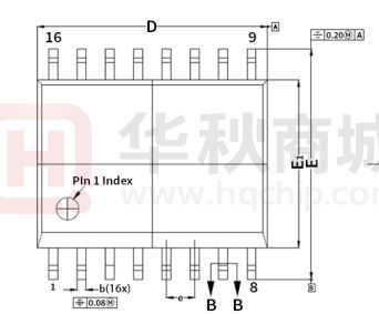
Figure 9.1 SOP16(300mil)/SOW16 Package Shape and Dimension in millimeters
Figure 9.2 SOP16(300mil)/SOW16 Package Board Layout Example
Copyright © 2023, NOVOSENSE
Page 26
�NSi8260/NSi8261/NSi8262/NSi8263
Datasheet (EN) 1.6
Figure 9.3 SSOP16 Package Shape and Dimension in millimeters
Figure 9.4 SSOP16 Package Board Layout Example
Copyright © 2023, NOVOSENSE
Page 27
�NSi8260/NSi8261/NSi8262/NSi8263
Datasheet (EN) 1.6
Figure 9.5 SOP16(150mil) Package Shape and Dimension in millimeters
Figure 9.6 SOP16(150mil) Package Board Layout Example
Copyright © 2023, NOVOSENSE
Page 28
�NSi8260/NSi8261/NSi8262/NSi8263
Datasheet (EN) 1.6
10. Order Information
Part
Number
NSi8260W
0-DSWR
NSi8260W
1-DSWR
NSi8261W
0-DSWR
NSi8261W
1-DSWR
NSi8262W
0-DSWR
NSi8262W
1-DSWR
NSi8263W
0-DSWR
NSi8263W
1-DSWR
NSi8260S
0-DSSR
NSi8260S
1-DSSR
NSi8261S
0-DSSR
NSi8261S
1-DSSR
NSi8262S
0-DSSR
NSi8262S
1-DSSR
NSi8263S
0-DSSR
NSi8263S
1-DSSR
NSi8260N
0-DSPNR
NSi8260N
1- DSPNR
NSi8261N
0- DSPNR
NSi8261N
1- DSPNR
NSi8262N
0- DSPNR
NSi8262N
1- DSPNR
NSi8263N
0- DSPNR
NSi8263N
1- DSPNR
Isolatio
n Rating
(kV)
5
Number
of side 1
inputs
6
Number
of side 2
inputs
0
Max Data
Rate
(Mbps)
150
Default
Output
State
Low
Temperature
MSL
Package
Type
Package
Drawing
SPQ
-55 to 125℃
2
SOW16
1000
5
6
0
150
High
-55 to 125℃
2
SOW16
1000
5
5
1
150
Low
-55 to 125℃
2
SOW16
1000
5
5
1
150
High
-55 to 125℃
2
SOW16
1000
5
4
2
150
Low
-55 to 125℃
2
SOW16
1000
5
4
2
150
High
-55 to 125℃
2
SOW16
1000
5
3
3
150
Low
-55 to 125℃
2
SOW16
1000
5
3
3
150
High
-55 to 125℃
2
SOW16
1000
3
6
0
150
Low
-55 to 125℃
1
SOP16
(300mil)
SOP16
(300mil)
SOP16
(300mil)
SOP16
(300mil)
SOP16
(300mil)
SOP16
(300mil)
SOP16
(300mil)
SOP16
(300mil)
SSOP16
SSOP16
2500
3
6
0
150
High
-55 to 125℃
1
SSOP16
SSOP16
2500
3
5
1
150
Low
-55 to 125℃
1
SSOP16
SSOP16
2500
3
5
1
150
High
-55 to 125℃
1
SSOP16
SSOP16
2500
3
4
2
150
Low
-55 to 125℃
1
SSOP16
SSOP16
2500
3
4
2
150
High
-55 to 125℃
1
SSOP16
SSOP16
2500
3
3
3
150
Low
-55 to 125℃
1
SSOP16
SSOP16
2500
3
3
3
150
High
-55 to 125℃
1
SSOP16
SSOP16
2500
3
6
0
150
Low
-55 to 125℃
1
SOP16
2500
3
6
0
150
High
-55 to 125℃
1
SOP16
2500
3
5
1
150
Low
-55 to 125℃
1
SOP16
2500
3
5
1
150
High
-55 to 125℃
1
SOP16
2500
3
4
2
150
Low
-55 to 125℃
1
SOP16
2500
3
4
2
150
High
-55 to 125℃
1
SOP16
2500
3
3
3
150
Low
-55 to 125℃
1
SOP16
2500
3
3
3
150
High
-55 to 125℃
1
SOP16
(150mil)
SOP16
(150mil)
SOP16
(150mil)
SOP16
(150mil)
SOP16
(150mil)
SOP16
(150mil)
SOP16
(150mil)
SOP16
(150mil)
SOP16
2500
Copyright © 2023, NOVOSENSE
Page 29
�NSi8260/NSi8261/NSi8262/NSi8263
Datasheet (EN) 1.6
NOTE: All packages are RoHS-compliant with peak reflow temperatures of 260 °C according to the JEDEC industry standard
classifications and peak solder temperatures.
Part Number Rule:
NSi(82)(6)(1)(W)(1)-DSWR
Series Number
6=6Channels
Reverse Channel Amount:
N=N Channels N=0,1,2…
Package Type:
S= SSOP
W= WB
N=NB
Package Type:
SS=SSOP16
SW=SOP16(300mil)
SPN=SOP16(150mil)
D = Industrial
Q1 = Auto
Fail-Safe Output State:
0 = Logic Low
1 = Logic High
11. Documentation Support
Part Number
Product Folder
Datasheet
NSi826x
tbd
tbd
Copyright © 2023, NOVOSENSE
Technical
Documents
tbd
Isolator selection
guide
tbd
Page 30
�NSi8260/NSi8261/NSi8262/NSi8263
Datasheet (EN) 1.6
12. Tape and Reel Information
Figure 12.1 Reel Information (for all packages)
Copyright © 2023, NOVOSENSE
Page 31
�NSi8260/NSi8261/NSi8262/NSi8263
Datasheet (EN) 1.6
Direction of Feed
1
2
3
4
Quadrant
Designations
Copyright © 2023, NOVOSENSE
Figure 12.2 Tape Information of SOP16(300mil)
Page 32
�NSi8260/NSi8261/NSi8262/NSi8263
Datasheet (EN) 1.6
Direction of Feed
1
2
3
4
Quadrant
Designations
Copyright © 2023, NOVOSENSE
Figure 12.3 Tape Information of SSOP16
Page 33
�NSi8260/NSi8261/NSi8262/NSi8263
Datasheet (EN) 1.6
Direction of Feed
1
2
3
4
Quadrant
Designations
Copyright © 2023, NOVOSENSE
Figure 12.4 Tape Information of SOP16(150mil)
Page 34
�NSi8260/NSi8261/NSi8262/NSi8263
Datasheet (EN) 1.6
13. Revision history
Revision
1.0
1.1
1.2
1.3
1.4
1.5
1.6
Description
Initial version
Changed tape and reel information
Updated Safety Regulatory
Updated Safety-Limiting Values. Update SSOP16 Package Shape
and Dimension in millimeters. Changed AEC-Q100 description.
Update SOW16\SSOP16 Package Board Layout Example
Update SSOP16 CTI and VDE file.
Update SOP16 Package, Typical Supply Current Equations
Copyright © 2023, NOVOSENSE
Date
2020/11/13
2020/12/20
2021/6/28
2022/4/25
2022/6/6
2023/1/12
2023/3/22
Page 35
�NSi8260/NSi8261/NSi8262/NSi8263
Datasheet (EN) 1.6
IMPORTANT NOTICE
The information given in this document shall in no event be regarded as any warranty or authorization of, express or
implied, including but not limited to accuracy, completeness, merchantability, fitness for a particular purpose or
infringement of any third party’s intellectual property rights.
You are solely responsible for your use of Novosense’ products and applications, and for the safety thereof. You shall
comply with all laws, regulations and requirements related to Novosense’s products and applications, although information
or support related to any application may still be provided by Novosense.
The resources are intended only for skilled developers designing with Novosense’ products. Novosense reserves the
rights to make corrections, modifications, enhancements, improvements or other changes to the products and services
provided. Novosense authorizes you to use these resources exclusively for the development of relevant applications
designed to integrate Novosense’s products. Using these resources for any other purpose, or any unauthorized
reproduction or display of these resources is strictly prohibited. Novosense shall not be liable for any claims, damages,
costs, losses or liabilities arising out of the use of these resources.
For further information on applications, products and technologies, please contact Novosense (www.novosns.com ).
Suzhou Novosense Microelectronics Co., Ltd
Copyright © 2023, NOVOSENSE
Page 36
�