SLG5NT1586V
Ultra-small 22.5 mΩ 2.5 A
Integrated Power Switch with Reverse Blocking
General Description
Pin Configuration
The SLG5NT1586V is a 22.5 mΩ 2.5 A single-channel load
switch that is able to switch 1 to 5 V power rails. The product
is packaged in an ultra-small 1.0 x 1.6 mm package.
1
ON
2
D
3
D
4
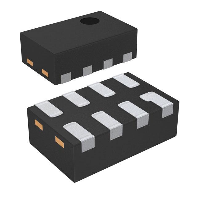
• 1.0 x 1.6 x 0.55 mm STDFN 8L package (2 fused pins for
drain and 2 fused pins for source)
• Logic level ON pin capable of supporting 0.85 V CMOS
Logic
• 22.5 mΩ RDSONwhile supporting 2.5 A
• Power Good Output
• Pb-Free / Halogen-Free / RoHS compliant
• Operating Temperature: -40 °C to 85°C
• Operating Voltage: 1.5 V to 5.5 V
SLG5NT1586V
Features
VDD
8
GND
7
PG
6
S
5
S
8-pin STDFN
(Top View)
Applications
• Notebook Power Rail Switching
• Tablet Power Rail Switching
• Smartphone Power Rail Switching
Block Diagram
2.5 A @ 22.5 mΩ
Reverse
Blocking
D
VDD
+1.5 to 5.5 V
S
Charge
Pump
Linear Ramp
Control
ON
Silego Technology, Inc.
000-005NT1586-100
PG
D
CMOS Input
Rev 1.00
Revised March 1, 2016
�SLG5NT1586V
Pin Description
Pin #
Pin Name
Type
Pin Description
1
VDD
PWR
VDD power for load switch control (1.5 V to 5.5 V)
2
ON
Input
Turns MOSFET ON (4 MΩ pull down resistor)
CMOS input with VIL < 0.3 V, VIH > 0.85 V
3
D
MOSFET
Drain of Power MOSFET (fused with pin 4)
4
D
MOSFET
Drain of Power MOSFET (fused with pin 3)
5
S
MOSFET
Source of Power MOSFET (fused with pin 6)
6
S
MOSFET
Source of Power MOSFET (fused with pin 5)
7
PG
Output
8
GND
GND
Power Good Output. Active High. Pin drives HIGH when VOUT > 95% VIN
Ground
Ordering Information
Part Number
Type
Production Flow
SLG5NT1586V
STDFN 8L
Industrial, -40 °C to 85 °C
SLG5NT1586VTR
STDFN 8L (Tape and Reel)
Industrial, -40 °C to 85 °C
000-005NT1586-100
Page 2 of 8
�SLG5NT1586V
Absolute Maximum Ratings
Parameter
VDD
TS
ESDHBM
WDIS
Description
Conditions
Power Supply
Storage Temperature
ESD Protection
Human Body Model
Min.
Typ.
Max.
Unit
--
--
7
V
-65
--
150
°C
2000
--
--
V
--
--
0.4
W
--
--
3.5
A
Package Power Dissipation
MOSFET IDSPK Peak Current from Drain to Source For no more than 1 ms with 1% duty cycle
Note: Stresses greater than those listed under “Absolute Maximum Ratings” may cause permanent damage to the device. This is a stress rating
only and functional operation of the device at these or any other conditions above those indicated in the operational sections of this
specification is not implied. Exposure to absolute maximum rating conditions for extended periods may affect reliability.
Electrical Characteristics
TA = -40 °C to 85 °C (unless otherwise stated)
Parameter
Description
Conditions
VDD
Power Supply Voltage
-40 °C to 85 °C
IDD
Power Supply Current (PIN 1)
RDSON
IDS
ISDLKG
VD
Static Drain to Source
ON Resistance
Operating Current
ISD Leakage
(Reverse Blocking Enabled)
when OFF
Min.
Typ.
Max.
Unit
1.5
--
5.5
V
--
--
1
μA
when ON, No load
--
14
30
μA
TA 25°C @ 100 mA
--
22.5
25
mΩ
TA 70°C @ 100 mA
--
25.6
30
mΩ
TA 85°C @ 100 mA
--
25.6
30
mΩ
VD = 1.0 V to 5.5 V
--
--
2.5
A
VS = 1. 0 V to 5.5 V, VD = 0 V,
VDD = 0 V, @ 25°C
--
0.29
0.50
μA
VS = 1. 0 V to 5.5 V, VD = 0 V,
VDD = 0 V, @ 85°C
--
0.85
1.30
μA
VS = 1. 0 V to 5.5 V, VD = 0 V,
VDD = 0 V, @ -40°C
--
3.35
5.00
μA
1.0
--
VDD
V
0
300
500
μs
Drain Voltage
TON_Delay
ON pin Delay Time
50% ON to Ramp Begin
TTotal_ON
Total Turn On Time
Example: VDD = VD = 5 V,
Source_Cap = 10 μF, RL = 20 Ω
2.1
2.6
3.1
ms
Slew Rate
Example: VDD = VD = 5 V,
Source_Cap = 10 μF, RL = 20 Ω
1.4
1.95
2.2
V/ms
--
--
500
μF
TSLEWRATE
CAPSOURCE Source Cap
Source to GND
ON_VIH
High Input Voltage on ON pin
0.85
--
VDD
V
ON_VIL
Low Input Voltage on ON pin
-0.3
0
0.3
V
VOL
High Output Voltage on PG pin
VDD = 5 V, IOL = -0.1 mA
--
--
0.4
V
VOH
High Output Voltage on PG pin
VDD = 5 V, IOH = 0.1 mA
VDD-0.4
--
VDD
V
Thermal shutoff turn-on temperature
--
125
--
°C
THERMOFF Thermal shutoff turn-off temperature
--
100
--
°C
THERMON
THERMTIME Thermal shutoff time
TOFF_Delay
OFF Delay Time
PGTRIGGER Power Good Trigger Level
--
--
1
ms
50% ON to VS Fall, VDD = VD = 5 V
--
8
--
μs
VOUT % of VIN
--
92
--
%
Notes:
1. Refer to table for configuration details.
000-005NT1586-100
Page 3 of 8
�SLG5NT1586V
TTotal_ON, TON_Delay and Slew Rate Measurement
ON
50% ON
50% ON
TOFF_DELAY
90% VS
VS
90% VS
TON_DELAY
10% VS
10% VS
Slew Rate (V/ms)
TFALL
TTotal_ON
000-005NT1586-100
Page 4 of 8
�SLG5NT1586V
Package Top Marking System Definition
ABC
Serial Number
Pin 1 Identifier
000-005NT1586-100
Page 5 of 8
�SLG5NT1586V
Package Drawing and Dimensions
8 Lead STDFN Package 1.0 x 1.6 mm (Fused Lead)
IC Net Weight: 0.0025 g
000-005NT1586-100
Page 6 of 8
�SLG5NT1586V
Tape and Reel Specifications
Max Units
Leader (min)
Nominal
Reel &
Package # of
Package Size
Hub Size
Length
Type
Pins
per Reel per Box
Pockets
[mm]
[mm]
[mm]
STDFN 8L
1x1.6mm
0.4P FC
Green
8
1.0 x 1.6 x 0.55
3,000
3,000
178 / 60
100
400
Trailer (min)
Pockets
Length
[mm]
Tape
Width
[mm]
100
400
8
Part
Pitch
[mm]
4
Carrier Tape Drawing and Dimensions
Pocket BTM Pocket BTM
Package
Length
Width
Type
STDFN 8L
1x1.6mm
0.4P FC
Green
Pocket
Depth
Index Hole
Pitch
Pocket
Pitch
Index Hole
Diameter
Index Hole Index Hole
to Tape
to Pocket Tape Width
Edge
Center
A0
B0
K0
P0
P1
D0
E
F
W
1.12
1.72
0.7
4
4
1.55
1.75
3.5
8
Recommended Reflow Soldering Profile
Please see IPC/JEDEC J-STD-020: latest revision for reflow profile based on package volume of 0.88 mm3 (nominal). More
information can be found at www.jedec.org.
000-005NT1586-100
Page 7 of 8
�SLG5NT1586V
Revision History
Date
Version
03/01/2016
1.00
000-005NT1586-100
Change
Production Release
Page 8 of 8
�
很抱歉,暂时无法提供与“SLG5NT1586VTR”相匹配的价格&库存,您可以联系我们找货
免费人工找货