矽睿
Document #:
13-52-20 Title: QMA6100P Preliminary Datasheet
Rev: A1
Abstract
3-Axis Accelerometer QMA6100P
Advanced Information
The QMA6100P is a three-axis accelerometer. This surface-mount, small sized chip has integrated acceleration
transducer with signal conditioning ASIC, sensing tilt, motion, shock and vibration, targeted for applications such as
screen rotation, step counting, sleep monitor, gaming and personal navigation in mobile and wearable smart devices.
The QMA6100P is based on the state-of-the-art, high resolution single crystal silicon MEMS technology. Along with
custom-designed 14-bit ADC ASIC, it offers the advantages of low noise, high accuracy, low power consumption, and offset
trimming. The device supports digital interface I2C and SPI.
The QMA6100P is in a 2x2x0.95 mm3 surface mount 12-pin land grid array (LGA) package.
FEATURES
3-Axis Accelerometer in a 2x2x0.95 mm3 Land
Grid Array Package (LGA), guaranteed to
operate over a temperature range of -40 °C to
+85 °C.
14-Bit ADC with low noise accelerometer
sensor
I C Interface with SDR modes.
2
Support SPI digital interface
Built-In Self-Test
BENEFIT
Small size for highly integrated products.
Signals have been digitized and factory
trimmed.
High resolution allows for motion and tilt
sensing
High-Speed Interfaces for fast data
communications.
Enables low-cost functionality test after
assembly in production
Wide range operation voltage (1.71V to 3.6V)
and low power consumption (5-44uA low
power conversion current)
Automatically maintains sensor’s sensitivity
under wide operation voltage range and
compatible with battery powered
applications
Integrated FIFO with depth of 64 frames
RoHS compliant, halogen-free
Environmental protection and wide
Built–in motion algorithm
Low power and easy applications including
applications
step counting, sleep monitor, gaming and
personal navigation
�矽睿
Document #:
13-52-20 Title: QMA6100P Preliminary Datasheet
Rev: A1
CONTENTS
CONTENTS....................................................................................................................................................................................... 2
1
INTERNAL SCHEMATIC DIAGRAM ................................................................................................................................... 3
1.1
Internal Schematic Diagram ..................................................................................................................................... 3
2
SPECIFICATIONS AND I/O CHARACTERISTICS .............................................................................................................. 3
2.1
Product Specifications .............................................................................................................................................. 3
2.2
Absolute Maximum Ratings ..................................................................................................................................... 4
2.3
I/O Characteristics .................................................................................................................................................... 5
3
PACKAGE PIN CONFIGURATIONS ..................................................................................................................................... 5
3.1
Package 3-D View .................................................................................................................................................... 5
3.2
Package Outlines ...................................................................................................................................................... 7
4
EXTERNAL CONNECTION ................................................................................................................................................... 8
4.1
I2C Single Supply connection .................................................................................................................................. 8
4.2
SPI Single Supply connection .................................................................................................................................. 8
5
BASIC DEVICE OPERATION ................................................................................................................................................ 9
5.1
Acceleration sensor................................................................................................................................................... 9
5.2
Power Management .................................................................................................................................................. 9
5.3
Power On/Off Time ................................................................................................................................................ 10
5.4
Communication Bus Interface I2C and Its Addresses ............................................................................................. 11
6
MODES OF OPERATION ..................................................................................................................................................... 11
6.1
Modes Transition .................................................................................................................................................... 11
6.2
Description of Modes ............................................................................................................................................. 12
7
Functions and interrupts .......................................................................................................................................................... 12
7.1
STEP_ INT ............................................................................................................................................................. 13
7.2
DRDY_INT ............................................................................................................................................................ 13
7.3
ANY_MOT_INT .................................................................................................................................................... 14
7.4
SIG_MOT_INT ...................................................................................................................................................... 16
7.5
NO_MOT_INT ....................................................................................................................................................... 16
7.6
TAP_INT ................................................................................................................................................................ 17
7.7
RAISE_INT ............................................................................................................................................................ 18
7.8
FIFO_INT ............................................................................................................................................................... 18
7.9
Interrupt configuration ............................................................................................................................................ 19
8
I2C COMMUNICATION PROTOCOL .................................................................................................................................. 21
8.1
I2C Timings ............................................................................................................................................................ 21
8.2
I2C R/W Operation ................................................................................................................................................. 21
8.3
Serial Peripheral Interface(SPI) .............................................................................................................................. 23
9
REGISTERS ........................................................................................................................................................................... 26
9.1
Register Map .......................................................................................................................................................... 26
9.2
Register Definition ................................................................................................................................................. 28
The information contained herein is the exclusive property of QST, and shall not be distributed,
reproduced, or disclosed in whole or in part without prior written permission of QST.
2 / 37
�矽睿
Document #:
13-52-20 Title: QMA6100P Preliminary Datasheet
Rev: A1
1 INTERNAL SCHEMATIC DIAGRAM
1.1 Internal Schematic Diagram
Sinc
FS
Offset
SDM
G-SENSOR
CVA
INT1
Interrupt
Gain
INT2
AD0
IF
(I2C/SPI)
VPMXYZ
BG
OSC
FIFO
SDX
Reg File
SCX
OTP
SENB
GND
POWER(A+D)
POR
Mode
FSM
SelfTest
Block Diagram
Table 1.
Block Function
Block
Transducer
CVA
Interrupt
FSM
I2C/SPI
OSC
Power
VDD
GND
Figure 1.
RESV2
Function
3-axis acceleration sensor
Charge-to-Voltage amplifier for sensor signals
Digital interrupt engine, to generate interrupt signal on data conversion, and
motion function
Finite state machine, to control device in different mode
Interface logic data I/O
Oscillator for internal operation
Power block, including LDO
2 SPECIFICATIONS AND I/O CHARACTERISTICS
2.1
Product Specifications
Table 2.
Specifications (* Tested and specified at 25°C and 3.0V VDD except stated otherwise.)
The information contained herein is the exclusive property of QST, and shall not be distributed,
reproduced, or disclosed in whole or in part without prior written permission of QST.
3 / 37
�矽睿
Parameter
Supply voltage VDD
Standby current
Low power current
Low noise current
Document #:
13-52-20 Title: QMA6100P Preliminary Datasheet
Conditions
VDD, for internal blocks
VDD and VDDIO on
ODR=800 Hz
ODR=400 Hz
ODR=200 Hz
ODR=80 Hz
ODR=50Hz
ODR=25 Hz
ODR=12.5 Hz
ODR=6.25 Hz
Min
1.71
Data output rate
(ODR)
Max
3.6
Unit
V
μA
μA
μA
1.25
1000
Samples
/sec
Startup time
From the time when VDD reaches to
90% of final value to the time when
device is ready for conversion
2
ms
Wakeup time
From the time device enters into
active mode to the time device is
ready for conversion
1
ms
Operating
temperature
Acceleration Full
Range
Sensitivity
Sensitivity
Temperature Drift
Sensitivity tolerance
Zero-g offset
Zero-g offset
Temperature Drift
Noise density
Nonlinearity
Cross Axis Sensitivity
2.2
Typ
3.3
0.5
38
19
10
5
149
75
38
19
Rev: A1
-40
±2/±4/±8/
±16/±32
4096
2048
1024
512
256
FS=±2g
FS=±4g
FS=±8g
FS=±16g
FS=±32g
℃
85
g
LSB/g
FS=±2g, Normal VDD Supplies
±0.02
%/℃
Gain accuracy
FS=±2g, Normal VDD Supplies
±4
±80
%
mg
FS=±2g, Normal VDD Supplies
±2
mg/℃
FS=±2g, run state
FS=±2g, Best fit straight line,
220
±0.5
1
μg/√Hz
%FS
%
Absolute Maximum Ratings
Table 3.
Absolute Maximum Ratings (Tested at 25°C except stated otherwise.)
Item
Power Supply Voltage
Input Voltage (other than power)
Reflow Classificaition
Storage Temperature
Symbol Min
Max
Unit
Vddmax -0.3
5.4
V
Vmax
-0.2 Vdd+0.2
V
MSL3, 260℃ Peak Temperature
℃
Tstr
-50
150
The information contained herein is the exclusive property of QST, and shall not be distributed,
reproduced, or disclosed in whole or in part without prior written permission of QST.
Remark
4 / 37
�矽睿
Document #:
13-52-20 Title: QMA6100P Preliminary Datasheet
Storage Humidity
ESD(HBM)
ESD(MM)
ESD(CDM)
Shock Immunity
Hstr
Vhbm
Vmm
Vcdm
10
95
±2000
±200
±500
10000
%RH
V
V
V
g
Rev: A1
duration < 200uS
2.3 I/O Characteristics
Table 4.
I/O Characteristics
Item
Digital Input Low Voltage
Digital Input High Voltage
Digital Input Hysterisis
Digital Output Low Voltage(I2C)
Digital Output Low Voltage (SPI)
Digital Output High Voltage1
(SPI)
(Vio>=1.62V)
Digital Output High Voltage2
(SPI)
(Vio>=1.2V)
Leakage Current at Output OFF
Internal Pullup Resistor
I2C Load Capacitor
Load Capacitance of
Reset Terminal
Pulse Width of
Asynchronous Reset
Power on Startup Time
Symbol
Vil_d
Vih_d
Vidhys
Vol_d1
Vol_d2
Condition
Min
Vddio*0.8
Vddio*0.1
0
0
Typ
-
Max
Vddio*0.2
Vddio*0.2
Vddio*0.2
Unit
V
V
V
V
V
Vddio*0.8
-
-
V
Vddio*0.6
-
-
V
-10
-
10
70
120
190
-
-
400
µA
koh
m
pF
Crst
-
-
20
pF
Trst
100
-
-
µsec
Tstart
-
-
10
msec
Io=3mA (SDI) *1)
Io=1mA (SDI, SDO) *1)
Voh_d1
Io=1mA (SDI, SDO) *1)
Voh_d2
Ioff
Rpullup
Cb
Io=1mA (SDI, SDO) *1)
SDX, AD0
SENB
SDX, SCX
3 PACKAGE PIN CONFIGURATIONS
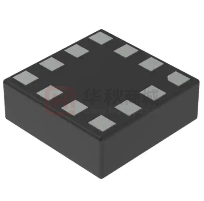
3.1 Package 3-D View
Arrow indicates direction of g field that generates a positive output reading in normal measurement configuration.
Z
X
QMA6100P
Y
The information contained herein is the exclusive property of QST, and shall not be distributed,
reproduced, or disclosed in whole or in part without prior written permission of QST.
5 / 37
�Document #:
矽睿
Figure 2.
Package View
Table 5.
Pin Configurations
13-52-20 Title: QMA6100P Preliminary Datasheet
No
Name
IO
Description
1
2
3
4
5
6
7
8
9
10
11
12
AD0
SDX
VDD
RESV1
INT1
INT2
NC
GNDIO
GND
SENB
RESV2
SCX
I
I/O
P
A
O
O
NC
G
G
I
A
I
LSB of I2C address, or SDO of SPI serial data output
SDA of I2C serial data, or SDI of SPI serial data input
Power supply to internal circuitry
Reserved
Interrupt1
Interrupt2
Not connected
Ground to IO
Ground to internal circuitry
Protocol selection
Reserved
SCL of I2C serial clock, or SCK of SPI serial clock
No
Name
IO
1
2
3
4
5
6
AD0
SDX
VDD
RESV1
INT1
INT2
I
I/O
P
A
O
O
I2C
VDDIO/GND
SDA
VDD
Float/GND
INT1
INT2
Rev: A1
Logic Level
Connectivity
SPI_3W
Float
SDI/SDO
VDD
Float/GND
INT1
INT2
VDDIO
VDDIO
NA
NA
VDDIO
VDDIO
NA
GND
NA
VDDIO
NA
VDDIO
SPI_4W
MISO
MOSI
VDD
Float/GND
INT1
INT2
The information contained herein is the exclusive property of QST, and shall not be distributed,
reproduced, or disclosed in whole or in part without prior written permission of QST.
6 / 37
�矽睿
7
8
9
10
11
12
NC
GNDIO
GND
SENB
RESV2
SCX
NC
G
G
I
A
I
Document #:
NC
GND
GND
VDDIO/Float
VDDIO/Float/GND
SCL
13-52-20 Title: QMA6100P Preliminary Datasheet
NC
GND
GND
CSB
VDDIO/Float/GND
SCK
Rev: A1
NC
GND
GND
CSB
VDDIO/Float/GND
SCK
3.2 Package Outlines
3.2.1
Package Type
LGA (Land Grid Array)
3.2.2
Package Outline Drawing
2.0mm (Length)*2.0mm (Width)*0.95mm (Height)
NOTE:
1. CONTROLLING DIMENSION: MILLIMETER.
Figure 3.
3.2.3
Package Outline Drawing
Tape And Reel
Devices are shipped in reels, in standard cardboard box packaging.
Package
Reel Size
WidthxPitch
Qty/reel
Trailer(Inner
layer Min length)
LGA(2x2)
13”
12*4
5000
300mm
Leader(Outer
layer Min length
300mm
The information contained herein is the exclusive property of QST, and shall not be distributed,
reproduced, or disclosed in whole or in part without prior written permission of QST.
Pin 1 Location
Up Right
7 / 37
�矽睿
4
4.1
Document #:
13-52-20 Title: QMA6100P Preliminary Datasheet
Rev: A1
EXTERNAL CONNECTION
I2C Single Supply connection
P
Figure 4.
4.2
I2C Single Supply Connection
SPI Single Supply connection
The information contained herein is the exclusive property of QST, and shall not be distributed,
reproduced, or disclosed in whole or in part without prior written permission of QST.
8 / 37
�矽睿
Document #:
13-52-20 Title: QMA6100P Preliminary Datasheet
Rev: A1
P
Figure 5.
SPI Single Supply Connection
5 BASIC DEVICE OPERATION
5.1
Acceleration sensor
The QMA6100P acceleration sensor circuit consists of tri-axial sensors and application specific support circuits to measure
the acceleration of device. When a DC power supply is applied to the sensor, the sensor converts any accelerating incident in
the sensitive axis directions to charge output.
5.2
Power Management
Device has one power supply pins. VDD is the main power supply for all of the internal blocks, including analog and digital.
The device contains a power-on-reset generator. It generates reset pulse as power on, which can load the register’s default
value, for the device to function properly.
To make sure the POR block functions well, we should have such constrains on the timing of VDD
The information contained herein is the exclusive property of QST, and shall not be distributed,
reproduced, or disclosed in whole or in part without prior written permission of QST.
9 / 37
�矽睿
Document #:
13-52-20 Title: QMA6100P Preliminary Datasheet
Rev: A1
The device should turn-on both power pins in order to operate properly. When the device is powered on, all registers are
reset by POR, then the device transits to the standby mode and waits for further commends.
Table 6 provides references for four power states.
Table 6. Power States
Power State
1
2
5.3
VDD
0V
1.71V-3.6V
Power State Description
Device off
Device on, normal operation mode, enters standby mode
after POR
Power On/Off Time
Device has one power supply pins and two ground pins. VDD is the main power supply for all of the internal blocks,
including analog and digital. GND is 0V supply for all of internal blocks, and GNDIO for digital interface.
There is no limitation on the voltage levels of VDD , as long as it is within operating range.
The device contains a power-on-reset generator. It generates reset pulse as power on, which can load the register’s default
value, for the device to function properly.
To make sure the POR block functions well, we should have such constrains on the timing of VDD.
The power on/off time related to the device is in Table 7
Table 7. Time Required for Power On/Off
Parameter
POR Completion
Time
Symbol
PORT
Power off Voltage
SDV
Power on Interval
PINT
Power on Time
PSUP
Condition
Time Period After VDD and
VDDIO at Operating Voltage to
Ready for I2C Commend and
Analogy Measurement.
Voltage that Device Considers to
be Power Down.
Time Period Required for Voltage
Lower Than SDV to Enable Next
POR
Time Period Required for Voltage
from SDV to 90% of final value
Min.
Typ.
Max.
250
Unit
μs
0.2
V
100
The information contained herein is the exclusive property of QST, and shall not be distributed,
reproduced, or disclosed in whole or in part without prior written permission of QST.
μs
50
ms
10 / 37
�矽睿
Figure 9.
5.4
Document #:
13-52-20 Title: QMA6100P Preliminary Datasheet
Rev: A1
Power On/Off Timing
Communication Bus Interface I2C and Its Addresses
This device will be connected to a serial interface bus as a slave device under the control of a master device, such as the
processor. Control of this device is carried out via I²C.
This device is compliant with I²C -Bus Specification, document number: 9398 393 40011. As an I²C compatible device, this
device has a 7-bit serial address and supports I²C protocols. This device supports standard and fast speed modes, 100 kHz
and 400 kHz, respectively. External pull-up resistors are required to support all these modes.
There are two I2C addresses selected by connecting pin 1 (AD0) to GND or VDD.
to “001001” and the LSB can be configured by AD0.
Table 8.
The first six MSB are hardware configured
I2C Address Options
AD0 (pin 1)
Connect to GND
Connect to VDD
I2C Slave Address (HEX)
12
13
I2C Slave Address (BIN)
0010010
0010011
6 MODES OF OPERATION
6.1
Modes Transition
QMA6100P has two different operational modes, controlled by register (0x11), MODE_BIT. The main purpose of these
modes is for power management. The modes can be transited from one to another, as shown below, through I2C
commands. The default mode after power-on is standby mode.
The information contained herein is the exclusive property of QST, and shall not be distributed,
reproduced, or disclosed in whole or in part without prior written permission of QST.
11 / 37
�Document #:
矽睿
13-52-20 Title: QMA6100P Preliminary Datasheet
Rev: A1
Power Off
Reset
(POR or Soft Reset)
Reset
(POR or Soft Reset)
NVM Load
NVM Load
0x36=0xB6
0x36=0xB6
Standby
Standby
0x11=1
0x11=1
0x33=1
Active
0x33=1
0x11=0
Active
0x11=0
0x36=0xB6
0x36=0xB6
Figure 10.
Basic operation flow after power-on
Figure 11.
The work mode transferring
The default mode after power on is standby mode. Through I2C instruction, device can switch between standby mode and
active mode. With SOFTRESET by writing 0xB6 into register 0x36, all of the registers will get default values. SOFTRESET can
be done both in active mode and in standby mode. Also, by writing 1 in NVM_LOAD (0x33) when device is in active
mode, the NVM related image registers will get default value from NVM, however, other registers will keep the values of
their own.
6.2 Description of Modes
6.2.1
Active Mode
In active mode, the ADC digitizes the charge signals from transducer, and digital signal processor conditions these signals in
digital domain, processes the interrupts, and send data to Data registers (0x01~0x06) and FIFO (accessible through register
0x3F).
6.2.2
Standby Mode
In standby mode, most of the blocks are off, while device is ready for access through I2C. Standby mode is the default mode
after power on or soft reset. Device can enter into this mode by set the soft reset register (0x36) to 0xB6 or set the
MODE_BIT (0x11) to logic 0.
7 Functions and interrupts
ASIC support interrupts, such as STEP_INT, DRDY_INT, ANY_MOT_INT, SIG_MOT_INT, NO_MOT_INT, RAISE_INT and
FIFO_INT, etc.
The information contained herein is the exclusive property of QST, and shall not be distributed,
reproduced, or disclosed in whole or in part without prior written permission of QST.
12 / 37
�矽睿
Document #:
13-52-20 Title: QMA6100P Preliminary Datasheet
Rev: A1
7.1 STEP_ INT
The STEP_FPAG detect that the user is entering/exiting step mode. When the user enters into step mode, at least one axis
sensor data will vary periodically, by numbering the variation periods and the acceleration intensity the step counter can be
calculated.
Figure 10.
STEP SIGNAL
The related interrupt status bit is STEP_INT (0x0A) and SIG_STEP (0x0A). When the interrupt is generated, the value
of STEP_INT will be set to logic 1, which will be cleared after the interrupt status register is read by user.
STEP_IEN/SIG_STEP_IEN (0x16/0x16) is the enable bit for the STEP_INT/SIG_STEP_INT. Also, to get this interrupt on
PIN_INT1 and/or PIN_INT2, we need to set INT1_STEP (0x19)/INT1_SIG_STEP (0x19)
or INT2_STEP (0x1B)
/INT2_SIG_STEP (0x1B) to logic 1, to map the internal interrupt to the interrupt PINs.
7.2 DRDY_INT
The width of the acceleration data is 14 bits, in two’s complement representation. The data of each axis is split into 2 parts,
the MSB part (one byte contains bit 13 to bit 6) and the LSB part (one byte contains bit 5 to bit 0). Reading data should start
with LSB part. When user is reading the LSB byte of data, to ensure the integrity of the acceleration data, the content of
MSB can be locked, by setting SHADOW_DIS (0x21) to logic 0. This lock function can be disabled by setting SHADOW_DIS
to logic 1. Without lock, the MSB and LSB content will be updated by new value immediately. The bit NEW_DATA in the LSB
byte is the flag of the new data. If new data is updated, this NEW_DATA flag will be 1, and will be cleared when
corresponding MSB or LSB is read by user.
Also, the user should note that even with SHADOW_DIS=0, the data of 3 axes are not guaranteed from the same time point.
The device supports four different acceleration measurement ranges. The range is setting through RANGE (0x0F), and
the details as following:
Acceleration
RANGE
Resolution
range
0001
2g
244ug/LSB
0010
4g
488ug/LSB
0100
8g
977ug/LSB
The information contained herein is the exclusive property of QST, and shall not be distributed,
reproduced, or disclosed in whole or in part without prior written permission of QST.
13 / 37
�矽睿
1000
1111
Others
Document #:
13-52-20 Title: QMA6100P Preliminary Datasheet
16g
32g
2g
Rev: A1
1.95mg/LSB
3.91mg/LSB
244ug/LSB
The interrupt for the new data serves for the synchronous data reading for the host. It is generated after storing a new
value of z-axis acceleration data into data register. This interrupt will be cleared automatically when the next data
conversion cycle starts, and the interrupt will be effective about 64*MCLK, and automatically cleared.
The interrupt mode for the new data is fixed to be non-latched.
7.3 ANY_MOT_INT
Any motion Any motion detection uses slope between two successive data to detect the changes in motion. It generates
interrupt when a preset threshold ANY_MOT_TH (0x2E) is exceeded.
The time difference between two successive data depends on the output data rate (ODR).
Slope(t1) = (𝑎𝑐𝑐(𝑡1) − 𝑎𝑐𝑐(𝑡0)) ∗ 𝑂𝐷𝑅
The any motion detection criteria are fulfilled and interrupt is generated if any of enabled channels exceeds ANY_MOT_TH
for ANY_MOT_DUR (0x2C) consecutive times.
As long as all the enabled channels data fall or stay below ANY_MOT_TH for ANY_MOT_DUR consecutive times, the
interrupt will be reset unless the interrupt signal is latched.
The any motion detection engine will send out the signals of axis which triggered the interrupt (ANY_MOT_FIRST_X
(0x09), ANY_MOT_FIRST_Y (0x09), ANY_MOT_FIRST_Z (0x09)) and the sign of the motion (ANY_MOT_SIGN
(0x09))
The information contained herein is the exclusive property of QST, and shall not be distributed,
reproduced, or disclosed in whole or in part without prior written permission of QST.
14 / 37
�矽睿
Document #:
13-52-20 Title: QMA6100P Preliminary Datasheet
Rev: A1
acceleration
time
slope
+threshould
time
-threshould
duration
duration
counter
duration
time
interrupt
time
There is an option for using any motion detector to detect high-g.
If the 0x2F (any_mot_in_sel) is logic-1, the input of any-motion detector would be acceleration, and the threshold range
would cover full scale range.
ANY_MOT_TH*16 LSB
0
Threshold of Any Motion
ANY_MOT_TH*32 LSB
Slope of Accel
1
0
Any Motion
Detector
Accel
1
any_mot_in_sel
any_mot_in_sel (0x2F) : 0 for any motion detection
1 for high-g detection
The information contained herein is the exclusive property of QST, and shall not be distributed,
reproduced, or disclosed in whole or in part without prior written permission of QST.
15 / 37
�矽睿
Document #:
13-52-20 Title: QMA6100P Preliminary Datasheet
Rev: A1
7.4 SIG_MOT_INT
A significant motion is a motion due to a change in user location.
The algorithm is as following:
1) Look for movement, same setting as any motion detection
2) If movement detected, sleep for T_Skip (0x2F)
3) Look for movement
a) If no movement detected within T_Proof (0x2F), go back to 1
b) If movement detected, report a significant movement, and generate the interrupt
The significant motion detection and any motion detection are exclusive, user can select either one through SIG_MOT_SEL
(0x2F).
If significant motion is detected, the engine will set SIG_MOT_INT (0x0A).
any-motion result
time
T_skip
(sleep)
T_proof
(detect)
interrupt
1/ODR
time
7.5 NO_MOT_INT
No-motion interrupt is generated if the slope (absolute value of acceleration difference) on all selected axes is smaller than
the programmable threshold for a programmable time. Figure shows the timing for the no-motion interrupt. Register (0x2C)
NO_MOT_DUR defines the delay times before the no-motion interrupt is generated. Table lists the delay times adjustable
with register (0x2C) NO_MOT_DUR.
The no-motion interrupt is enabled per axis by writing logic 1 to bits (0x18) NO_MOTION_EN_X, (0x18) NO_MOTION_EN_Y,
and (0x18) NO_MOTION_EN_Z, respectively. The no-motion threshold is set through the (0x2D) NO_MOT_TH register. The
meaning of an LSB of (0x2D) NO_MOT_TH depends on the selected g-range: it corresponds to 3.91mg in 2g-range (7.81mg
in 4g-range, 15.6mg in 8g-range, 31.25mg in 16g-range, 62.5mg in 32g-range). Therefore the maximum value is 996mg in
2g-range (2g in 4g-range, 4g in 8g-range, 8g in 16g-range, and 16g in 32g-range). The time difference between the
successive acceleration samples depends on the selected ODR and equates to 1/ODR.
The information contained herein is the exclusive property of QST, and shall not be distributed,
reproduced, or disclosed in whole or in part without prior written permission of QST.
16 / 37
�矽睿
Document #:
13-52-20 Title: QMA6100P Preliminary Datasheet
Rev: A1
acceleration
time
slope
+threshould
time
`
-threshould
duration
counter
duration
time
interrupt
time
7.6 TAP_INT
Tap detection allows the device to detect the events such as clicking or double clicking of a touch-pad. A tap event is detected if
a pre-defined slope of the acceleration. The tap detection includes single tap (S_TAP), double tap (D_TAP), triple tap (T_TAP), and
quadruple tap (Q_TAP). A ‘Single tap’ is a single event within a certain shock time, followed by a certain quiet time. A ‘double tap’
consists of a first such event followed by a second event within a defined time frame, and so on.
Each tap interrupt can be enabled (disabled) by setting ‘1’ (‘0’) to S_TAP_EN(0x16), D_TAP_EN(0x16),
T_TAP_EN(0x16), and Q_TAP_EN(0x16).
The status of each tap interrupt is stored in S_TAP_INT(0x0A), D_TAP_INT(0x0A), T_TAP_INT(0x0A), and
Q_TAP_INT(0x0B).
The shock and quiet threshold for detecting a tap event is set by register (0x2B) TAP_SHOCK_TH and (0x1E) TAP_QUIET_TH.
The meaning of threshold LSB is 31.25mg, the range is 0 ~ 2G.
The tap input selection is defined in (0x2B) TAP_IN_SEL, the default input is √𝑥 2 + 𝑦 2 + 𝑧 2 , the tap detector could only
detect 1 axis as shown below:
TAP_IN_SEL:
0: X-axis
1: Y-axis
2: Z-axis
3: √𝑥 2 + 𝑦 2 + 𝑧 2
In figure the timing for tap is visualized:
The information contained herein is the exclusive property of QST, and shall not be distributed,
reproduced, or disclosed in whole or in part without prior written permission of QST.
17 / 37
�矽睿
Document #:
13-52-20 Title: QMA6100P Preliminary Datasheet
Rev: A1
Slope
+Shock Threshould
+Quiet Threshould
-Quiet Threshould
time
-Shock Threshould
shock time
quiet time
shock time
quiet time
shock time
Single Tap Interrupt
quiet time
shock time
quiet time
duration time
duration time
duration time
12.5ms
time
Double Tap Interrupt
12.5ms
time
Triple Tap Interrupt
12.5ms
time
Quadruple Tap Interrupt
12.5ms
time
7.7 RAISE_INT
Raise wake algorithm is used to detect the action of raise hand (or hand down). The interrupt is enabled by writing logic 1 to
bits (0X16[1]) RAISE_EN, (0X16[2]) HD_EN. User can adjust the sensitivity through the registers. The register
RAISE_WAKE_SUM_TH(0X22[5:0]) defines the strength of hand action (raise and down). The register
RAISE_DIFF_TH(0X23[1:0],0X22[7:6]) defines the differential values of twice actions, when the hand behavior almost done
the differential value will be smaller and we can use this register to set the threshold. RAISE_WAKE_PERIOD and
RAISE_WAKE_TIMEOUT_TH define the duration of the total hand action.
7.8 FIFO_INT
This device has integrated FIFO memory, capable of storing up to 64 frames, with each frame contains three 14bits words,
for acceleration data of X, Y, and Z axis. All of the 3-axes acceleration is sampled at same time point
The FIFO can be configured as three modes, FIFO mode, STREAM mode, and BYPASS mode.
FIFO mode.
In FIFO mode, the acceleration data of selected axes are stored in the buffer memory. If enabled, a watermark interrupt can
be triggered when the buffer filled up to the defined level. The buffer will continuously be filled until the fill level reaches to
64. When the buffer is full, data collection stops, and the new data will be ignored. Also, FIFO_FULL interrupt will be
triggered when enabled.
STREAM mode
In STREAM mode, the acceleration data of selected axes will be stored into the buffer until the buffer is full. The buffer’s
depth is 64 now. when the buffer is full, data collection continues, and the oldest data is discarded. If enabled, a watermark
interrupt will be triggered when the fill level reached to the defined level. Also, when buffer is full, FIFO_FULL interrupt will
be triggered if enabled. If any old data is discarded, the FIFO_OR (0x0B) will be set to be logic 1.
BYPASS mode
In BYPASS mode, only the current acceleration data of selected axes can be read out from FIFO. The FIFO acts like the
STREAM mode when a depth of 1. Compared to reading directly from data register, this mode has the advantage of
ensuring the package of xyz data are from same time point. The data registers are updated sequentially and have chance for
The information contained herein is the exclusive property of QST, and shall not be distributed,
reproduced, or disclosed in whole or in part without prior written permission of QST.
18 / 37
�矽睿
Document #:
13-52-20 Title: QMA6100P Preliminary Datasheet
Rev: A1
xyz data are from different time. Also, if any old data is discarded, the FIFO_OR will be set to be logic 1, similar as that in
STREAM mode.
The FIFO mode can be configured by setting FIFO_MODE (0x3E).
FIFO_MODE
MODE
00
BYPASS
01
FIFO
10
STREAM
11
FIFO
User can select the acceleration data of which axes to be stored in FIFO. This configuration can be done by setting FIFO_CH
(0x3E)
If all of the 3-axes data are selected, the format of data read from 0x3F is as following
XLSB
XMSB
YLSB
YMSB
ZLSB
ZMSB
These comprise one frame
If only one axis is enabled, the format data read from 0x3F is as following
YLSB
YMSB
These comprise one frame
If the frame is not read completely, the remaining parts of the frame will be discarded.
If the FIFO is read beyond the FIFO fill level, all zeroes will be read out.
FIFO_FRAME_COUNTER (0x0E) reflects the current filled level of the buffer. If additional data frames are written into
the buffer when FIFO is full (in STREAM mode or BYPASS mode), then FIFO_OR (0x0B) is set to be logic 1. This FIFO_OR
bit can be considered as flag of discarding old data.
When a write access to one of the FIFO configuration registers (0x3E) or watermark registers (0x31) occurs, the FIFO buffer
will be cleared, the FIFO fill level indication register FIFO_FRAME_COUNTER (0x0E) will be cleared, and the FIFO_OR
(0x0B) will be cleared as well.
As mentioned above, FIFO controller contains two interrupts, FIFO_FULL interrupt and watermark interrupt. These two
interrupts are functional in all of the FIFO operating modes.
The watermark interrupt is triggered when the filled level of buffer reached to the level that is defined by register
FIFO_WM_LVL (0x31), if the interrupt is enabled by setting INT_FWM_EN (0x17) to logic 1 and INT1_FWM
(0x1A) or INT2_FWM (0x1C) is set.
The FIFO_FULL interrupt is triggered when the buffer has been fully filled. In FIFO mode, the filled level is 64, and in STREAM
mode the filled level is 64, in BYPASS mode the filled level is 1. To enable FIFO_FULL interrupt, INT_FFULL_EN (0x17)
should be set to 1, and INT1_FFULL (0x1A) and INT2_FFULL (0x1C) is set.
The status of watermark interrupt and FIFO full interrupt can be read through INT_STAT (0x0B)
After soft-reset, the watermark interrupt and FIFO full interrupt are disabled.
For the FIFO to recollect the data, user should reconfigure the register FIFO_MODE.
7.9 Interrupt configuration
The device has the above 3 interrupt engines. Each of the interrupts can be enabled and configured independently. If the
trigger condition of the enabled interrupt fulfilled, the corresponding interrupt status bit will be set to logic 1, and the
mapped interrupt pin will be activated. The device has two interrupt PINs, INT1 and INT2. Each of the interrupts can be
mapped to either PIN or both PINs.
The interrupt status registers INT_ST(0x09~0x0d) will update when a new data word is written into the data registers. If an
interrupt is disabled, the related active interrupt status bit is disabled immediately.
The information contained herein is the exclusive property of QST, and shall not be distributed,
reproduced, or disclosed in whole or in part without prior written permission of QST.
19 / 37
�矽睿
Document #:
13-52-20 Title: QMA6100P Preliminary Datasheet
Rev: A1
When interrupt condition is fulfilled, related bit of interrupt will be set, until the associated interrupt condition is no more
valid. Read operation to related register will also clear the register.
Device supports 2 interrupt modes, non-latched, and latched mode. The interrupt modes are set through LATCH_INT
(0x21).
In non-latched mode, the mapped interrupt pin will be set and/or cleared same as associated interrupt register bit. Also, the
mapped interrupt pin can be cleared with read operation to any of the INT_ST(0x09~0x0d).
Exception to this is the new data interrupt and step interrupt, which are automatically reset after a fixed time (T_Pulse =
64/MCLK), no matter LATCH_INT (0x21) is set to 0 or 1.
In latched mode, the clearings of mapped pins are determined by INT_RD_CLR (0x21).
If the condition for trigging the interrupt still holds, the interrupt status will be set again with the next change of the data
registers.
Mapping the interrupt pins can be set by INT_MAP (0x19~0x1B).
The electrical interrupt pins can be set INT_PIN_CONF (0x20). The active logic level can be set to 1 or 0, and the
interrupt pin can be set to open-drain or push-pull.
The information contained herein is the exclusive property of QST, and shall not be distributed,
reproduced, or disclosed in whole or in part without prior written permission of QST.
20 / 37
�矽睿
Document #:
13-52-20 Title: QMA6100P Preliminary Datasheet
Rev: A1
8 I2C COMMUNICATION PROTOCOL
8.1
I2C Timings
Table 9 and Figure 11 describe the I2C communication protocol times
Table 9.
I2C Timings
Parameter
SCL Clock
SCL Low Period
SCL High Period
SDA Setup Time
SDA Hold Time
Start Hold Time
Start Setup Time
Stop Setup Time
New Transmission
Time
Rise Time
Fall Time
Figure 11.
t sudat
t hddat
t hdsta
t susta
t susto
t buf
Condition
Min.
0
1
1
0.1
0
0.6
0.6
0.6
1.3
Typ.
Max.
400
Unit
kHz
μs
μs
0.9
tr
tf
μs
μs
μs
μs
μs
μs
μs
μs
I2C Timing Diagram
8.2
I2C R/W Operation
8.2.1
Abbreviation
Table 10.
Symbol
fscl
t low
t high
Abbreviation
The information contained herein is the exclusive property of QST, and shall not be distributed,
reproduced, or disclosed in whole or in part without prior written permission of QST.
21 / 37
�矽睿
SACK
MACK
NACK
RW
8.2.2
Document #:
13-52-20 Title: QMA6100P Preliminary Datasheet
Rev: A1
Acknowledged by slave
Acknowledged by master
Not acknowledged by master
Read/Write
Start/Stop/Ack
START: Data transmission begins with a high to transition on SDA while SCL is held high. Once I 2C transmission starts, the
bus is considered busy.
STOP: STOP condition is a low to high transition on SDA line while SCL is held high.
ACK: Each byte of data transferred must be acknowledged. The transmitter must release the SDA line during the
acknowledge pulse while the receiver must then pull the SDA line low so that it remains stable low during the high period of
the acknowledge clock cycle.
NACK: If the receiver doesn’t pull down the SDA line during the high period of the acknowledge clock cycle, it’s recognized
as NACK by the transmitter.
8.2.3
I2C Write
I C write sequence begins with start condition generated by master followed by 7 bits slave address and a write bit
(R/W=0). The slave sends an acknowledge bit (ACK=0) and releases the bus. The master sends the one-byte register
address. The slave again acknowledges the transmission and waits for 8 bits data which shall be written to the specified
register address. After the slave acknowledges the data byte, the master generates a stop signal and terminates the writing
protocol.
2
Table 11.
I2C Write
Slave Address
STOP
Data
(0x80)
1 0 0 0 0 0 0 0
SACK
Register Address
(0x11)
0 0 0 1 0 0 0 1
SACK
SACK
START
8.2.4
R
W
0 0 1 0 0 1 0 0
I2C Read
I C write sequence consists of a one-byte I2C write phase followed by the I2C read phase. A start condition must be
generated between two phases. The I2C write phase addresses the slave and sends the register address to be read. After
slave acknowledges the transmission, the master generates again a start condition and sends the slave address together
with a read bit (R/W=1). Then master releases the bus and waits for the data bytes to be read out from slave. After each
data byte the master has to generate an acknowledge bit (ACK = 0) to enable further data transfer. A NACK from the master
stops the data being transferred from the slave. The slave releases the bus so that the master can generate a STOP
condition and terminate the transmission.
The register address is automatically incremented and more than one byte can be sequentially read out. Once a new data
read transmission starts, the start address will be set to the register address specified in the current I 2C write command.
2
Table 12.
I2C Read
Slave Address
Data
(0x00)
SACK
Register Address
(0x00)
0 0 0 0 0 0 0 0
M
AC
K
R
W
SA
CK
ST
AR
T
Slave Address
SACK
START
R
W
0 0 1 0 0 1 0 0
Data
(0x01)
The information contained herein is the exclusive property of QST, and shall not be distributed,
reproduced, or disclosed in whole or in part without prior written permission of QST.
22 / 37
�矽睿
Data
(0x02)
0 0 0 0 0 0 1 0
……………………………….
Data
(0x07)
0 0 0 0 0 0 0 0
……………………………….
Rev: A1
STOP
0 0 0 0 0 0 0 0
NACK
0 0 0 0 0 0 1 0
MACK
0 0 1 0 0 1 0 1
MACK
MACK
8.3
13-52-20 Title: QMA6100P Preliminary Datasheet
Document #:
Serial Peripheral Interface(SPI)
The timing specification of SPI is given in the following table.
Table 13: SPI timing
Parameter
Clock Frequency
Symbol
fSPI
Condition
Max. load on SDI or
SDO=25pF
Min.
0
Max.
10
Unit
MHz
t SCKL
t SCKH
20
20
ns
SDI Setup Time
SDI Hold Time
SDO Output Delay
t SDI_setup
t SDI_hold
t SDO_OD
20
20
ns
ns
ns
ns
SENB Setup Time
SENB Hold Time
t SENB_setup
t SENB_hold
SCK Low Pulse
SCK High Pulse
ns
Load =25pF
Load =250pF,
Vddio =2.4V
30
40
20
40
ns
ns
The following figure shows the definition of SPI timing given in table 13:
tSENB_hold
tSENB_setup
SENB
SCK
tSCKL
tSCKH
SDI
tSDI_setup
tSDI_hold
SDO
tSDO_OD
Figure. 12 SPI timing diagram
The SPI interface of QMA6100P is compatible with two modes, ‘00’ and ‘11’. The automatic selection between mode ‘00’ and mode
‘11’ is done based on the value of SCK at the falling edge of SENB. Two configurations of SPI interface are supported by QMA6100P:
4-wire and 3-wire. The same protocol is used by both configurations. The device operates in 4-wire configuration by default. The
configuration can be switched to 3-wire configuration by setting EN_SPI3W(0x20[5])=1. Pin SDI is used as the common data pin in 3wire configuration.
The information contained herein is the exclusive property of QST, and shall not be distributed,
reproduced, or disclosed in whole or in part without prior written permission of QST.
23 / 37
�13-52-20 Title: QMA6100P Preliminary Datasheet
Document #:
矽睿
Rev: A1
For single byte read or write operation, 16-bit protocols are used. QMA6100P also supports multiple-byte read or write operations.
In 4-wire configuration, SENB(low active), SCK(serial clock), SDI(serial data input) and SDO(serial data output) pins are used. The
communication starts when SENB is pulled low by SPI master and stops when SENB is pulled high. SCK is also controlled by SPI
master. SDI and SDO are driven at the falling edge of SCK and should be captured at the rising edge of SCK.
The basic write operation waveform for 4-wire configuration is depicted below in figure 13. During the entire write cycle SDO
remains in high impedance state.
4-Wire SPI Write Timing Diagram (Mode 3)
SENB
SCK
SDI
R/W
A6
A5
A4
A3
A2
A1
A0
DI7
DI6
DI5
DI4
DI3
DI2
DI1
DI0
DI5
DI4
DI3
DI2
DI1
DI0
SDO
4-Wire SPI Write Timing Diagram (Mode 0)
SENB
SCK
SDI
R/W
A6
A5
A4
A3
A2
A1
A0
DI7
DI6
SDO
Bit 0 : R/W bit, R/W=0 : write mode; R/W=1 : read mode.
Bit 1-7 : 7-bit address of registers.
Bit 8-15 : Data DI7~DI0 (write mode). It is the data that will be written into the slave. (MSB first)
Bit 8-15 : Data DO7~DO0 (read mode). It is the data that will be read from the device. (MSB first)
Figure 13: 4-wire basic SPI Write sequence
The basic read operation waveform for 4-wire configuration is depicted in figure 14 below.
The information contained herein is the exclusive property of QST, and shall not be distributed,
reproduced, or disclosed in whole or in part without prior written permission of QST.
24 / 37
�13-52-20 Title: QMA6100P Preliminary Datasheet
Document #:
矽睿
Rev: A1
4-Wire SPI Read Timing Diagram (Mode 3)
SENB
SCK
SDI
R/W
A6
A5
A4
A3
A2
A1
A0
SDO
DI7
DI6
DI5
DI4
DI3
DI2
DI1
DI0
DO7
DO6
DO5
DO4
DO3
DO2
DO1
DO0
4-Wire SPI Read Timing Diagram (Mode 0)
SENB
SCK
SDI
R/W
A6
A5
A4
A3
A2
SDO
A1
A0
DI7
DI6
DI5
DI4
DI3
DI2
DI1
DI0
DO7
DO6
DO5
DO4
DO3
DO2
DO1
DO0
Bit 0 : R/W bit, R/W=0 : write mode; R/W=1 : read mode.
Bit 1-7 : 7-bit address of registers.
Bit 8-15 : Data DI7~DI0 (write mode). It is the data that will be written into the slave. (MSB first)
Bit 8-15 : Data DO7~DO0 (read mode). It is the data that will be read from the device. (MSB first)
Figure 14: 4-wire basic SPI Read sequence
The data bits are defined as follows:
Bit0: Read/Write bit. When 0, the data DI is written to the chip. When 1, the data DO is read from the chip.
Bit1-7: Address A(6:0).
Bit8-15: when in write mode, these are the data DI, which will be written to the address. When in read mode, these are the DO,
which are read from the address.
Multiple byte read/write operations are possible by keeping SENB low and continuing the data transfer. Only the first register
address has to be provided. Addresses are automatically incremented after each read/write access as long as SENB stays low.
The principle of multiple read/write is shown below.
The information contained herein is the exclusive property of QST, and shall not be distributed,
reproduced, or disclosed in whole or in part without prior written permission of QST.
25 / 37
�矽睿
Document #:
13-52-20 Title: QMA6100P Preliminary Datasheet
Rev: A1
Burst Read Timing Diagram
SENB
SCK
SDI
R, Index Address
DataR from
Regindex+1
DataR from
Regindex
SDO
DataR from
Regindex+2
Burst Write Timing Diagram
SENB
SCK
SDI
W, Index Address
Dataw to Regindex
Dataw to Regindex+1
Dataw to Regindex+2
SDO
Figure 15: SPI multiple byte Read/Write
In 3-wire configuration, SENB(low active), SCK(serial clock) and SDI(serial data input) pins are used. The communication starts when
SENB is pulled low by SPI master and stops when SENB is pulled high. SCK is also controlled by SPI master. SDI is driven at the falling
edge of SCK when used as input of the device and should be captured at the rising edge of SCK when used as the output of the
device.
3-Wire SPI Read/Write Timing Diagram (Mode 3)
SENB
SCK
SDI
R/W
A6
A5
A4
A3
A2
A1
A0
D7
D6
D5
D4
D3
D2
D1
D0
Bit 0 : R/W bit, R/W=0 : write mode; R/W=1 : read mode.
Bit 1-7: 7-bit address of registers.
Bit 8-15: R/W=0 : D7 ~ D0 are written into slave; R/W=1 : D7~D0 are read from slave. (MSB first).
Figure 16: 3-wire basic SPI Read/Write sequence
9 REGISTERS
9.1
Register Map
The information contained herein is the exclusive property of QST, and shall not be distributed,
reproduced, or disclosed in whole or in part without prior written permission of QST.
26 / 37
�Document #:
矽睿
13-52-20 Title: QMA6100P Preliminary Datasheet
Rev: A1
The table below provides a list of the 8-bit registers embedded in the device and their respective function and addresses
Table 14. Register Map
Add.
0x3F
0x3E
0x3D
0x3C
0x3B
0x3A
0x39
0x38
0x37
0x36
0x35
0x34
0x33
0x32
0x31
0x30
0x2F
0x2E
0x2D
0x2C
0x2B
0x2A
0x29
0x28
0x27
0x26
0x25
0x24
0x23
0x22
0x21
0x20
0x1F
0x1E
0x1D
0x1C
0x1B
0x1A
0x19
0x18
0x17
0x16
0x15
0x14
0x13
0x12
0x11
0x10
0x0F
0x0E
0x0D
0x0C
0x0B
0x0A
0x09
0x08
0x07
0x06
0x05
0x04
0x03
0x02
0x01
0x00
Name
FIFO_CFG
bit7
bit6
FIFO_MODE
IMAGE
OFFSET_X
S_RESET
Z_TH[3:0]
YZ_TH_SEL[2:0]
Internal
ST
FIFO_WM
RST_MOT
MOT_CFG
TAP
OS_CUST
na
INT_CFG
INT_PIN_CFG
STEP_CFG
INT_MAP
INT_EN
na
PM
BW
FSR
FIFO_ST
INT_ST
na
DATA
CHIP ID
bit5
bit4
bit3
bit2
bit1
FIFO_DATA
RAISE_XYZ_SW
FIFO_EN_Z
FIFO_EN_Y
GAIN_Z
GAIN_Y
GAIN_X
OFFSET_Z
OFFSET_Y
OFFSET_X
GAIN_Z
OFFSET_Y
SOFTRESET: 0xB6 / NVM_UNLOCK: 0xB3
X_TH[3:0]
Y_TH[4:0]
SELFTEST_BIT
SELFTEST_SIGN
bit0
FIFO_EN_X
STEP_BP_AXIS
FIFO_WTMK_LVL
MO_BP_LPF
RFF_BP_LPF
STEP_BP_LPF
TAP_RST_N
NO_MOT_RST_N SIG_MOT_RST_NANY_MOT_RST_N
SIG_MOT_TPROOF
SIG_MOT_TSKIP
SIG_MOT_SEL
ANY_MOT_TH
NO_MOT_TH
NO_MOT_DUR
ANY_MOT_DUR
TAP_IN_SEL
TAP_SHOCK_TH
TAP_DUR
TAP_QUIET
TAP_SHOCK
T_TAP_DELAY
TAP_EARIN
OS_CUST_Z
OS_CUST_Y
OS_CUST_X
RAISE_MODE
RAISE_WAKE_PERIOD[10:8]
RAISE_WAKE_TIMEOUT_TH[11:8]
RAISE_WAKE_PERIOD[7:0]
RAISE_WAKE_TIMEOUT_TH[7:0]
HD_Z_TH[2:0]
HD_X_TH[2:0]
RAISE_WAKE_DIFF_TH[3:2]
RAISE_WAKE_DIFF_TH[1:0]
RAISE_WAKE_SUM_TH[5:0]
LATCH_INT_STEP
INT_RD_CLR
SHADOW_DIS
DIS_I2C
LATCH_INT
DIS_PU_SENB
DIS_IE_AD0
EN_SPI3W STEP_COUNT_PEAK
INT2_OD
INT2_LVL
INT1_OD
INT1_LVL
STEP_START_CNT
STEP_COUNT_PEAK
STEP_COUNT_P2P
NLPF_STEP
TAP_QUIET_TH[5:0]
STEP_INTERVAL
EN_RESET_DC
INT2_NO_MOT
INT2_FWM
INT2_FFULL
INT2_DATA
INT2_Q_TAP INT2_ANY_MOT
INT2_S_TAP
INT2_SIG_STEP INT2_D_TAP
INT2_T_TAP
INT2_STEP
INT2_HD
INT2_RAISE
INT2_SIG_MOT
INT1_NO_MOT
INT1_FWM
INT1_FFULL
INT1_DATA
INT1_Q_TAP INT1_ANY_MOT
INT1_S_TAP
INT1_SIG_STEP INT1_D_TAP
INT1_T_TAP
INT1_STEP
INT1_HD
INT1_RAISE
INT1_SIG_MOT
NO_MOT_EN_Z NO_MOT_EN_Y NO_MOT_EN_X
ANY_MOT_EN_Z ANY_MOT_EN_Y ANY_MOT_EN_X
INT_FWM_EN INT_FFULL_EN INT_DATA_EN
S_TAP_EN
SIG_STEP_IEN
D_TAP_EN
T_TAP_EN
STEP_IEN
HD_EN
RAISE_EN
Q_TAP_EN
STEP_TIME_UP
STEP_TIME_LOW
STEP_CLR
STEP_PRECISION
STEP_EN
STEP_SAMPLE_CNT
T_RSTB_SINC_SEL
MCLK_SEL
MODE_BIT
NLPF
BW
RANGE
EN_16B
FIFO_FRAME_COUNTER
STEP_CNT
TAP_SIGN
FIFO_OR
FIFO_WM_INT FIFO_FULL_INT
DATA_INT
EARIN_FLAG
Q_TAP_INT
S_TAP_INT
SIG_STEP
D_TAP_INT
T_TAP_INT
STEP_INT
HD_INT
RAISE_INT
SIG_MOT_INT
NO_MOT
STEP_FLAG
ANY_MOT_SIGN ANY_MOT_FIRST_Z ANY_MOT_FIRST_Y ANY_MOT_FIRST_X
STEP_CNT
STEP_CNT
ACC_Z
ACC_Z
0
NEWDATA_Z
ACC_Y
ACC_Y
0
NEWDATA_Y
ACC_X
ACC_X
0
NEWDATA_X
CHIP ID to indicate the product version
ANY_MOT_IN_SEL
The information contained herein is the exclusive property of QST, and shall not be distributed,
reproduced, or disclosed in whole or in part without prior written permission of QST.
27 / 37
R/W
R
RW
RW
RW
RW
RW
RW
RW
RW
RW
RW
RW
RW
RW
RW
RW
RW
RW
RW
RW
RW
RW
RW
RW
RW
RW
RW
RW
RW
RW
RW
RW
RW
RW
RW
RW
RW
RW
RW
RW
RW
RW
RW
RW
RW
RW
RW
RW
RW
R
R
R
R
R
R
R
R
R
R
R
R
R
R
R
DEF
00
07
NVM
NVM
NVM
NVM
NVM
NVM
NVM
00
66
9D
05
00
00
3F
00
00
00
00
CD
05
00
00
00
02
81
00
7C
D8
00
05
A9
08
00
00
00
00
00
00
00
00
16
19
7F
14
00
00
00
00
00
00
00
00
00
00
00
00
00
00
00
00
00
ANA
�Document #:
矽睿
9.2
13-52-20 Title: QMA6100P Preliminary Datasheet
Rev: A1
Register Definition
Register 0x00 (CHIP ID)
Bit7
Bit6
Bit5
CHIP_ID
This register is used to identify the device
Register 0x01 ~ 0x02 (DXL, DXM)
Bit7
Bit6
Bit5
DX
DX
DX:
NEWDATA_X:
Bit4
Bit3
Bit2
Bit1
Bit0
R/W
RW
Default
0x90
Bit4
Bit3
Bit2
Bit1
Bit0
NEWDATA
_X
R/W
R
Default
0x00
R
0x00
R/W
R
Default
0x00
R
0x00
R/W
R
Default
0x00
R
0x00
Bit0
R/W
R
R
Default
0x00
0x00
14bits acceleration data of x-channel. This data is in two’s complement.
1, acceleration data of x-channel has been updated since last reading
0, acceleration data of x-channel has not been updated since last reading
Register 0x03 ~ 0x04 (DYL, DYM)
Bit7
Bit6
Bit5
DY
DY
DY:
NEWDATA_Y:
Bit4
Bit3
Bit2
Bit1
14bits acceleration data of y-channel. This data is in two’s complement.
1, acceleration data of y-channel has been updated since last reading
0, acceleration data of y-channel has not been updated since last reading
Register 0x05 ~ 0x06 (DZL, DZM)
Bit7
Bit6
Bit5
DZ
DZ
DZ:
NEWDATA_Z:
Bit4
Bit3
Bit2
Bit1
Register 0x09 (INT_ST0)
Bit7
Bit6
NO_MOT
STEP_FLAG
STEP_FLAG:
ANY_MOT_SIGN:
ANY_MOT_FIRST_Z:
ANY_MOT_FIRST_Y:
ANY_MOT_FIRST_X:
Bit0
NEWDATA
_Z
14bits acceleration data of z-channel. This data is in two’s complement.
1, acceleration data of z-channel has been updated since last reading
0, acceleration data of z-channel has not been updated since last reading
Register 0x07 ~ 0x08 (STEP_CNT)
Bit7
Bit6
Bit5
Bit4
Bit3
Bit2
Bit1
STEP_CNT
STEP_CNT
STEP_CNT:
16 bits of step counter, out of total 24bits data. The MSB data are in 0x0e
NO_MOT:
Bit0
NEWDATA
_Y
Bit5
Bit4
Bit3
ANY_MOT
_SIGN
Bit2
ANY_MOT
_FIRST_Z
Bit1
ANY_MOT
_FIRST_Y
Bit0
ANY_MOT
_FIRST_X
R/W
R
Default
0x00
Bit2
HD_INT
Bit1
RAISE_INT
Bit0
SIG_MOT_I
NT
R/W
R
Default
0x00
1, no_motion interrupt active
0, no_motion interrupt inactive
1, STEP detected
0, STEP not detected
1, sign of any_motion triggering signal is negative
0, sign of any_motion triggering signal is positive
1, any_motion interrupt is triggered by Z axis
0, any_motion interrupt is not triggered by Z axis
1, any_motion interrupt is triggered by Y axis
0, any_motion interrupt is not triggered by Y axis
1, any_motion interrupt is triggered by X axis
0, any_motion interrupt is not triggered by X axis
Register 0x0a (INT_ST1)
Bit7
Bit6
S_TAP_INT
SIG_STEP
Bit5
D_TAP_INT
Bit4
T_TAP_INT
Bit3
STEP_INT
The information contained herein is the exclusive property of QST, and shall not be distributed,
reproduced, or disclosed in whole or in part without prior written permission of QST.
28 / 37
�矽睿
S_TAP_INT:
SIG_STEP:
D_TAP_INT:
STEP_INT:
T_TAP_INT:
HD_INT:
RAISE_INT:
SIG_MOT_INT:
13-52-20 Title: QMA6100P Preliminary Datasheet
Document #:
Rev: A1
1, single tap is active
0, single tap is inactive
1, significant step is active
0, significant step is inactive
1, double tap is active
0, double tap is inactive
1, step valid interrupt is active
0, step quit interrupt is inactive
1, triple tap is active
0, triple tap is inactive
1, hand down interrupt is active
0, hand down interrupt is inactive
1, raise hand interrupt is active
0, raise hand interrupt is inactive
1, significant interrupt is active
0, significant interrupt is inactive
Register 0x0b (INT_ST2)
Bit7
Bit6
Bit5
Bit4
Bit3
FIFO_OR
FIFO_WM_ FIFO_FULL
DATA_INT
INT
_INT
FIFO_OR:
1, FIFO Over-Run occurred
0, FIFO Over-Run not occurred
FIFO_WM_INT:
1, FIFO watermark interrupt is active
0, FIFO watermark interrupt is inactive
FIFO_FULL_INT:
1, FIFO full interrupt is active
0, FIFO full interrupt is inactive
DATA_INT:
1, data ready interrupt active
0, data ready interrupt inactive
EARIN_FLAG:
1, ear-in interrupt is active
0, ear-in interrupt is inactive
Q_TAP_INT:
1, quad tap is active
0, quad tap is inactive
Bit2
Bit1
EARIN_FLA
G
Register 0x0c (INT_ST3)
Bit7
Bit6
Bit5
Bit4
Bit3
TAP_SIGN
TAP_SIGN:
1, tap sign is along with positive direction
0, tap sign is along with negative direction
Bit2
Bit0
Q_TAP_INT
Bit1
Register 0x0d (INT_ST4)
Bit7
Bit6
Bit5
Bit4
Bit3
Bit2
Bit1
STEP_CNT
STEP_CNT:
8bit MSB data of step counter, out of total 24bits data. The LSB data are in 0x07 and 0x08
R/W
R
Default
0x00
Bit0
R/W
R
Default
0x00
Bit0
R/W
R
Default
0x00
Register 0x0e (FIFO_ST)
Bit7
Bit6
Bit5
Bit4
Bit3
Bit2
Bit1
Bit0
R/W
Default
FIFO_FRAME_COUNTER
R
0x00
FIFO_FRAME_COUNTER: Fill level of FIFO buffer. An empty FIFO corresponds to 0x00. The frame counter can be cleared by reading out all of the frames, or by
writing register 0x3e (FIFO_CFG1) or 0x31.
Register 0x0f (FSR)
Bit7
Bit6
Bit5
Bit4
Bit3
Bit2
LPF_HPF
RANGE
RANGE:
set the full scale of the accelerometer. Setting as following
RANGE
0001
0010
0100
1000
1111
Others
Acceleration range
2g
4g
8g
16g
32g
2g
Bit1
Bit0
R/W
RW
Default
0x00
Resolution
244ug/LSB
488g/LSB
977ug/LSB
1.95mg/LSB
3.91mg/LSB
244ug/LSB
The information contained herein is the exclusive property of QST, and shall not be distributed,
reproduced, or disclosed in whole or in part without prior written permission of QST.
29 / 37
�矽睿
Document #:
Register 0x10 (BW)
Bit7
Bit6
Bit5
Bit4
HPF[2]
NLPF
BW
NLPF:
00: no LPF.
01: NLPF=2.
10: NLPF=4.
11: NLPF=8
BW:
bandwidth setting, as following
13-52-20 Title: QMA6100P Preliminary Datasheet
Bit3
Bit2
Bit1
Bit0
R/W
RW
Default
0xE0
Bit5
Bit4
Bit3
Bit2
Bit1
T_RSTB_SINC_SEL
MCLK_SEL
1, set device into active mode
0, set device into standby mode
T_RSTB_SINC_SEL: Reset clock setting. The preset time is reserved for CIC filter in digital
MCLK_SEL:
set the master clock to digital
Bit0
R/W
RW
Default
0x00
Register 0x11 (PM)
Bit7
Bit6
MODE_BIT
MODE_BIT:
Rev: A1
Register 0x12 (STEP_CONF0)
Bit7
Bit6
Bit5
Bit4
Bit3
Bit2
Bit1
Bit0
R/W
Default
STEP_EN
STEP_SAMPLE_CNT
RW
0x14
STEP_EN:
enable step counter, this bit should be set 1 when using step counter
STEP_SAMPLE_CNT:
sample count setting to renew dynamic threshold. The actual value is STEP_SAMPLE_CNT*8, default is 0xC, 96 sample count
Register 0x13 (STEP_CONF1)
Bit7
Bit6
Bit5
Bit4
Bit3
Bit2
STEP_CLR
STEP_PRECISION
STEP_CLR:
clear step count in register 0x0D ,0x08 and 0x07
STEP_PRECISION: algorithm setting
Register 0x14 (STEP_CONF2)
Bit7
Bit6
Bit5
STEP_TIME_LOW
STEP_TIME_LOW: algorithm setting
Register 0x15 (STEP_CONF3)
Bit7
Bit6
Bit5
STEP_TIME_UP
STEP_TIME_UP:
algorithm setting
Bit1
Bit0
R/W
RW
Default
0x7F
Bit4
Bit3
Bit2
Bit1
Bit0
R/W
RW
Default
0x19
Bit4
Bit3
Bit2
Bit1
Bit0
R/W
RW
Default
0x00
Bit2
HD_EN
Bit1
RAISE_EN
Bit0
Q_TAP_EN
R/W
RW
Default
0x00
Register 0x16 (INT_EN0)
Bit7
Bit6
Bit5
Bit4
Bit3
S_TAP_EN
SIG_STEP_I D_TAP_EN
T_TAP_EN
STEP_IEN
EN
S_TAP_EN:
1, enable single tap
0, disable single tap
SIG_STEP_IEN:
1, enable significant step interrupt
0, disable significant step interrupt
D_TAP_EN:
1, enable double tap
0, disable double tap
T_TAP_EN:
1, enable triple tap
0, disable triple tap
STEP_IEN:
1, enable step valid interrupt
0, disable step valid interrupt
HD_EN:
1, enable hand-down interrupt
0, disable hand-down interrupt
RAISE_EN:
1, enable raise-hand interrupt
0, disable raise-hand interrupt
Q_TAP_EN:
1, enable quad tap
0, disable quad tap
Register 0x17 (INT_EN1)
The information contained herein is the exclusive property of QST, and shall not be distributed,
reproduced, or disclosed in whole or in part without prior written permission of QST.
30 / 37
�矽睿
Document #:
13-52-20 Title: QMA6100P Preliminary Datasheet
Bit7
Bit6
Bit5
Bit4
Bit3
INT_FWM_ INT_FFULL
INT_DATA
EN
_INT
_EN
INT_FWM_EN:
1, enable FIFO watermark interrupt
0, disable FIFO watermark interrupt
INT_FFULL_EN:
1, enable FIFO full interrupt
0, disable FIFO full interrupt
INT_DATA_EN:
1, enable data ready interrupt
0, disable data ready interrupt
Register 0x18 (INT_EN2)
Bit7
Bit6
Bit5
Bit4
Bit3
NO_MOT_
NO_MOT_
NO_MOT_
EN_Z
EN_Y
EN_X
NO_MOT_EN_Z:
1, enable no_motion interrupt on Z axis
0, disable no_motion interrupt on Z axis
NO_MOT_EN_Y:
1, enable no_motion interrupt on Y axis
0, disable no_motion interrupt on Y axis
NO_MOT_EN_X:
1, enable no_motion interrupt on X axis
0, disable no_motion interrupt on X axis
ANY_MOT_EN_Z:
1, enable any_motion interrupt on Z axis
0, disable any_motion interrupt on Z axis
ANY_MOT_EN_Y:
1, enable any_motion interrupt on Y axis
0, disable any_motion interrupt on Y axis
ANY_MOT_EN_X:
1, enable any_motion interrupt on X axis
0, disable any_motion interrupt on X axis
Bit2
Bit1
Bit0
R/W
RW
Default
0x00
Bit2
ANY_MOT
_EN_Z
Bit1
ANY_MOT
_EN_Y
Bit0
ANY_MOT
_EN_X
R/W
RW
Default
0x00
Bit1
INT1_RAIS
E
Bit0
INT1_SIG_
MOT
R/W
RW
Default
0x00
Bit1
INT1_Q_TA
P
Bit0
INT1_ANY_
MOT
R/W
RW
Default
0x00
Register 0x19 (INT_MAP0)
Bit7
Bit6
Bit5
Bit4
Bit3
Bit2
INT1_S_TA
INT1_SIG_
INT1_D_TA INT1_T_TA
INT1_STEP
INT1_HD
P
STEP
P
P
INT1_S_TAP:
1, map single tap interrupt to INT1 pin
0, not map single tap interrupt to INT1 pin
INT1_SIG_STEP:
1, map significant step interrupt to INT1 pin
0, not map significant step interrupt to INT1 pin
INT1_D_TAP:
1, map double tap interrupt to INT1 pin
0, not map double tap interrupt to INT1 pin
INT1_T_TAP:
1, map triple tap interrupt to INT1 pin
0, not map triple tap interrupt to INT1 pin
INT1_STEP:
1, map step valid interrupt to INT1 pin
0, not map step valid interrupt to INT1 pin
INT1_HD:
1, map hand down interrupt to INT1 pin
0, not map hand down interrupt to INT1 pin
INT1_RAISE:
1, map raise hand interrupt to INT1 pin
0, not map raise hand interrupt to INT1 pin
INT1_SIG_MOT:
1, map significant interrupt to INT1 pin
0, not map significant interrupt to INT1 pin
Register 0x1a (INT_MAP1)
Bit7
Bit6
Bit5
Bit4
Bit3
Bit2
INT1_NO_
INT1_FWM INT1_FFUL
INT1_DAT
MOT
L
A
INT1_NO_MOT:
1, map no_motion interrupt to INT1 pin
0, not map no_motion interrupt to INT1 pin
INT1_FWM:
1, map FIFO watermark interrupt to INT1 pin
0, not map FIFO watermark interrupt to INT1 pin
INT1_FFULL:
1, map FIFO full interrupt to INT1 pin
0, not map FIFO full interrupt to INT1 pin
INT1_DATA:
1, map data ready interrupt to INT1 pin
0, not map data ready interrupt to INT1 pin
INT1_Q_TAP:
1, map quad tap interrupt to INT1 pin
0, not map quad tap interrupt to INT1 pin
INT1_ANY_MOT:
1, map any motion interrupt to INT1 pin
The information contained herein is the exclusive property of QST, and shall not be distributed,
reproduced, or disclosed in whole or in part without prior written permission of QST.
Rev: A1
31 / 37
�Document #:
矽睿
13-52-20 Title: QMA6100P Preliminary Datasheet
Rev: A1
0, not map any motion interrupt to INT1 pin
Register 0x1b (INT_MAP2)
Bit7
Bit6
Bit5
Bit4
Bit3
Bit2
INT2_S_TAP
INT2_SIG_S INT2_D_ INT2_T_TA
INT2_STEP
INT2_HD
TEP
TAP
P
INT2_S_TAP:
1, map single tap interrupt to INT2 pin
0, not map single tap interrupt to INT2 pin
INT2_SIG_STEP:
1, map significant step interrupt to INT2 pin
0, not map significant step interrupt to INT2 pin
INT2_D_TAP:
1, map double tap interrupt to INT2 pin
0, not map double tap interrupt to INT2 pin
INT2_T_TAP:
1, map triple tap interrupt to INT2 pin
0, not map triple tap interrupt to INT2 pin
INT2_STEP:
1, map step valid interrupt to INT2 pin
0, not map step valid interrupt to INT2 pin
INT2_HD:
1, map hand down interrupt to INT2 pin
0, not map hand down interrupt to INT2 pin
INT2_RAISE:
1, map raise hand interrupt to INT2 pin
0, not map raise hand interrupt to INT2 pin
INT2_SIG_MOT:
1, map significant interrupt to INT2 pin
0, not map significant interrupt to INT2 pin
Register 0x1c (INT_MAP3)
Bit7
Bit6
Bit5
Bit4
Bit3
Bit2
INT2_NO_
INT2_FWM INT2_FFUL
INT2_DAT
MOT
L
A
INT2_NO_MOT:
1, map no_motion interrupt to INT2 pin
0, not map no_motion interrupt to INT2 pin
INT2_FWM:
1, map FIFO watermark interrupt to INT2 pin
Bit1
INT2_RAISE
Bit1
INT2_Q_TA
P
Bit0
INT2_SI
G_MOT
Bit0
INT2_ANY_
MOT
R/W
RW
R/W
RW
Default
0x00
Default
0x00
0, not map FIFO watermark interrupt to INT2 pin
INT2_FFULL:
INT2_DATA:
INT2_Q_TAP:
INT2_ANY_MOT:
1, map FIFO full interrupt to INT2 pin
0, not map FIFO full interrupt to INT2 pin
1, map register data ready interrupt to INT2 pin
0, not map register data ready interrupt to INT2 pin
1, map quad tap interrupt to INT2 pin
0, not map quad tap interrupt to INT2 pin
1, map any motion interrupt to INT2 pin
0, not map any motion interrupt to INT2 pin
Register 0x1d (STEP_CFG0)
Bit7
Bit6
Bit5
STEP_INTERVAL
STEP_INTERVAL : algorithm setting
Bit4
Bit3
Bit2
Bit1
Bit0
Register 0x1e (STEP_CFG1)
Bit7
Bit6
Bit5
Bit4
Bit3
Bit2
Bit1
Bit0
NLPF_STEP
TAP_QUIET
NLPF_STEP:
Moving Average of Step: 1/2/4/8
TAP_QUIET_TH:
Tap quiet threshold selection, LSB of TAP_QUIET_TH is 31.25mg in all full scale.
Register 0x1f
Bit7
Bit6
STEP_START_CNT
STEP_START_CNT:
STEP_COUNT_PEAK:
STEP_COUNT_P2P:
Bit5
Bit4
Bit3
STEP_COUNT_PEAK
algorithm setting
algorithm setting
algorithm setting
Register 0x20 (INTPIN_CONF)
Bit7
Bit6
Bit5
DIS_PU_SE
DIS_IE_AD
EN_SPI3W
NB
0
Bit4
STEP_COU
NT_PEAK<
2>
Bit3
INT2_OD
R/W
RW
Default
0x00
R/W
RW
Default
0x08
Bit2
Bit1
STEP_COUNT_P2P
Bit0
R/W
RW
Default
0xA9
Bit2
INT2_LVL
Bit0
INT1_LVL
R/W
RW
Default
0x05
Bit1
INT1_OD
The information contained herein is the exclusive property of QST, and shall not be distributed,
reproduced, or disclosed in whole or in part without prior written permission of QST.
32 / 37
�矽睿
Document #:
13-52-20 Title: QMA6100P Preliminary Datasheet
Rev: A1
DIS_PU_SENB:
1, disable pull-up resistor of PIN_SENB
0, enable pull-up resistor of PIN_SENB
DIS_IE_AD0:
1, disable input of AD0
0, not disable input of AD0
EN_SPI3W:
1, enable 3W SPI
0, 4W SPI
STEP_COUNT_PEAK:
Definition in 0x1F
INT2_OD:
1, open-drain for INT2 pin
0, push-pull for INT2 pin
INT2_LVL:
1, logic high as active level for INT2 pin
0, logic low as active level for INT2 pin
INT1_OD:
1, open-drain for INT1 pin
0, push-pull for INT1 pin
INT1_LVL:
1, logic high as active level for INT1 pin
0, logic low as active level for INT1 pin
Register 0x21 (INT_CFG)
Bit7
Bit6
Bit5
Bit4
Bit3
Bit2
Bit1
Bit0
R/W
INT_RD_CL SHADOW_
DIS_I2C
LATCH_INT LATCH_INT RW
R
DIS
_STEP
INT_RD_CLR:
1, clear all the interrupts in latched-mode, when any read operation to any of registers from 0x09 to 0x0D
0, clear the related interrupts, only when read the register INT_ST (0x09 to 0x0D),
no matter the interrupts in latched-mode, or in non-latched-mode.
Reading 0x09 will clear the register 0x09 only and the others keep the status
SHADOW_DIS:
1, disable the shadowing function for the acceleration data
0, enable the shadowing function for the acceleration data.
When shadowing is enabled, the MSB of the acceleration data is locked,
when corresponding LSB of the data is reading.
This can ensure the integrity of the acceleration data during the reading.
The MSB will be unlocked when the MSB is read.
DIS_I2C:
1: disable I2C. Setting this bit to 1 in SPI mode is recommended
0: enable I2C
LATCH_INT_STEP: 1, step related interrupt is in latch mode
0, step related interrupt is in non-latch mode
LATCH_INT:
1, interrupt is in latch mode
0, interrupt is in non-latch mode
Register 0x22
Bit7
Bit6
Bit5
Bit4
RAISE_WAKE_DIFF_TH
RAISE_WAKE_SUM_TH
RAISE_WAKE_DIFF_TH: Threshold = 0 ~ 31.5 (LSB 0.5)
RAISE_WAKE_SUM_TH:
0
0.2
1
0.3
2
0.4
3
0.5
4
0.6
5
0.7
6
0.8
7
0.9
8
1.0
9
1.1
10
1.2
default
0.2
Bit3
Register 0x23
Bit7
Bit6
Bit5
Bit4
Bit3
HD_Z_TH
HD_X_TH
HD_Z_TH: hand down z threshold, 0~7
HD_X_TH: hand down x threshold, 0~7
RAISE_WAKE_DIFF_TH: Threshold = 0 ~ 31.5 (LSB 0.5)
Bit2
Bit2
Bit1
Bit0
Bit1
Bit0
RAISE_WAKE_DIFF_TH
Default
0x0C
R/W
RW
Default
0xD8
R/W
RW
Default
0x7C
Register 0x24
The information contained herein is the exclusive property of QST, and shall not be distributed,
reproduced, or disclosed in whole or in part without prior written permission of QST.
33 / 37
�矽睿
Document #:
13-52-20 Title: QMA6100P Preliminary Datasheet
Bit7
Bit6
Bit5
Bit4
Bit3
Bit2
Bit1
RAISE_WAKE_TIMEOUT_TH
RAISE_WAKE_TIMEOUT_TH:
Raise_wake_timeout_th[11:0] * ODR period = timeout count
Register 0x25
Bit7
Bit6
RAISE_WAKE_PERIOD
RAISE_WAKE_PERIOD:
Bit5
Bit4
Bit3
Bit2
Bit1
Rev: A1
Bit0
R/W
RW
Default
0x00
Bit0
R/W
RW
Default
0x00
Bit0
R/W
RW
Default
0x02
Raise_wake_period[10:0] * ODR period = wake count
Register 0x26
Bit7
Bit6
Bit5
Bit4
Bit3
Bit2
Bit1
RAISE_MODE RAISE_WAKE_PERIOD
RAISE_WAKE_TIMEOUT_TH
RAISE_MODE:
0:raise wake function, 1:ear-in function
RAISE_WAKE_PERIOD:
Raise_wake_period[10:0] * ODR period = wake count
RAISE_WAKE_TIMEOUT_TH: Raise_wake_timeout_th[11:0] * ODR period = timeout count
Register 0x27 (OS_CUST_X)
Bit7
Bit6
Bit5
Bit4
Bit3
Bit2
Bit1
Bit0
R/W
OS_CUST_X
RW
OS_CUST_X:
offset calibration of X axis for user, the LSB depends on full-scale of the device which is 3.9mg in 2g range,
7.8mg in 4g range, 15.6mg in 8g range, 31.2mg in 16g, and 62.5mg in 32g
Register 0x28 (OS_CUST_Y)
Bit7
Bit6
Bit5
Bit4
Bit3
Bit2
Bit1
Bit0
R/W
OS_CUST_Y
RW
OS_CUST_Y:
offset calibration of Y axis for user, the LSB depends on full-scale of the device which is 3.9mg in 2g range,
7.8mg in 4g range, 15.6mg in 8g range, 31.2mg in 16g, and 62.5mg in 32g
Register 0x29 (OS_CUST_Z)
Bit7
Bit6
Bit5
Bit4
Bit3
Bit2
Bit1
Bit0
R/W
OS_CUST_Z
RW
OS_CUST_Z:
offset calibration of Z axis for user, the LSB depends on full-scale of the device which is 3.9mg in 2g range,
7.8mg in 4g range, 15.6mg in 8g range, 31.2mg in 16g, and 62.5mg in 32g
Register 0x2a (RAISE_WAKE_SUM_TH RAISE_WAKE_DIFF_TH)
Bit7
Bit6
Bit5
Bit4
Bit3
Bit2
Bit1
Bit0
TAP_QUIET TAP_SHOC
TAP_DELA
TAP_EARIN
TAP_DUR
K
Y
TAP_QUIET:
1: Tap quiet time = 30ms 0: Tap quiet time = 20ms
TAP_SHOCK:
1: Tap shock time = 50ms 0: Tap shock time = 75ms
TAP_DELAY_Y:
0 : Triple tap interrupt would not wait for quadruple tap result.
1 : Triple tap interrupt would wait for quadruple tap result.
If quadruple tap is not toggle, triple tap would toggle after tap duration time finish.
TAP_EARIN:
1 : Tap enable would be related with EARIN_FLAG (reg 0x0B).
If EARIN_FLAG is low, tap detection will be disabled.
If EARIN_FLAG is high, tap detection is enabled by reg 0x16.
0 : Tap detection is enabled by reg 0x16.
TAP_DUR: Tap duration time selection
000: 100mS
001: 150mS
010: 200mS
011: 250mS
100: 300mS
101: 400mS
110: 500mS
111: 700mS
Register 0x2b (RAISE_WAKE_DIFF_TH HD_X_TH HD_Z_TH)
Bit7
Bit6
Bit5
Bit4
Bit3
TAP_IN_SEL
TAP_SHOCK_TH
Bit2
Bit1
Bit0
Default
0x00
Default
0x00
Default
0x00
R/W
RW
Default
0x05
R/W
RW
Default
0xCD
TAP_IN_SEL: Tap Detector Input Selection
The information contained herein is the exclusive property of QST, and shall not be distributed,
reproduced, or disclosed in whole or in part without prior written permission of QST.
34 / 37
�矽睿
TAP_SHOCK_TH:
Document #:
13-52-20 Title: QMA6100P Preliminary Datasheet
Rev: A1
0 : X-axis
1 : Y-axis
2 : Z-axis
3 : (X^2 + Y^2 + Z^2)^0.5
Tap shock threshold selection, LSB of TAP_SHOCK_TH is 31.25mg in all full scale.
Register 0x2c (MOT_CONF0)
Bit7
Bit6
Bit5
Bit4
Bit3
Bit2
Bit1
Bit0
R/W
Default
NO_MOT_DUR
ANY_MOT_DUR
RW
0x00
NO_MOT_DUR:
no motion interrupt will be triggered when slope < NO_MOT_TH for the times which defined by NO_MOT_DUR
Duration = (NO_MOT_DUR + 1) * 1s, if NO_MOT_DUR =b00
Duration = (NO_MOT_DUR + 4) * 5s, if NO_MOT_DUR =b01
Duration = (NO_MOT_DUR + 10) * 10s, if NO_MOT_DUR =b1x
ANY_MOT_DUR: any motion interrupt will be triggered when slope > ANY_MOT_TH for (ANY_MOT_DUR + 1) samples
Register 0x2d (MOT_CONF1)
Bit7
Bit6
Bit5
Bit4
Bit3
Bit2
Bit1
NO_MOT_TH
NO_MOT_TH:
Threshold of no-motion interrupt. The threshold definition is as following
TH= NO_MOT_TH * 16 * LSB
Register 0x2e (MOT_CONF2)
Bit7
Bit6
Bit5
Bit4
Bit3
Bit2
Bit1
ANY_MOT_TH
ANY_MOT_TH:
Threshold of any motion interrupt. The threshold definition is as following
ANY_MOT_IN_SEL = 0 : Threshold = ANY_MOT_TH * 16LSB
ANY_MOT_IN_SEL = 1 : Threshold = ANY_MOT_TH * 32LSB
ANT_MOT_IN_SEL is 0x2F.
Bit0
R/W
RW
Default
0x00
Bit0
R/W
RW
Default
0x00
Register 0x2f (MOT_CONF3)
Bit7
Bit6
Bit5
Bit4
Bit3
Bit2
Bit1
Bit0
R/W
RFF_BP_LP
ANY_MOT
SIG_MOT_TPROOF
SIG_MOT_TSKIP
SIG_MOT_
RW
F
_IN_SEL
SEL
RFF_BP_LP:
1: Data of register acceleration XYZ (0x01 ~ 0x06) and FIFO (0x3F) would bypass LPF.
0: Data of register file acceleration XYZ (0x01 ~ 0x06) and FIFO (0x3F) would be filtered by LPF.
ANY_MOT_IN_SEL:
0: Any-motion Input is Slope.
1: Any-motion Input is Acceleration, it could detect high-g.
SIG_MOT_TPROOF:
00, T_PROOF=0.25s
01, T_PROOF=0.5s
10, T_PROOF=1s
11, T_PROOF=2s
SIG_MOT_TSKIP:
00, T_SKIP=1.5s
01, T_SKIP=3s
10, T_SKIP=6s
11, T_SKIP=12s
SIG_MOT_SEL:
1, select significant motion interrupt
0, select any motion interrupt
Register 0x30
Bit7
MO_BP_LP
F
MO_BP_LPF:
Bit6
Bit5
Bit4
Bit3
Bit2
Bit1
STEP_BP_L
TAP_RST_
NO_MOT_
SIG_MOT_
PF
N
RST_N
RST_N
1: Input of any motion, sig motion and no motion would bypass LPF.
0: Input of any motion, significant motion and no motion would be filtered by LPF.
STEP_BP_LPF:
1: Input of step counter, raise wake, and tap detector would bypass LPF.
0: Input of step counter, raise wake, and tap detector would be filtered by LPF.
TAP_RST_N:
0, Reset tap detector. After reset, user should write 1 back.
NO_MOT_RST_N: 0, Reset no motion detector. After reset, user should write 1 back.
SIG_MOT_RST_N: 0, Reset significant motion detector. After reset, user should write 1 back.
ANY_MOT_RST_N: 0, Reset any motion detector. After reset, user should write 1 back.
Bit0
ANY_MOT
_RST_N
R/W
RW
Default
0x00
Default
0x1F
Register 0x31
Bit7
Bit6
Bit5
Bit4
Bit3
Bit2
Bit1
Bit0
R/W
Default
FIFO_WTMK_LVL
0x00
FIFO_WTMK_LVL: defines FIFO water mark level. Interrupt will be generated, when the number of entries in the FIFO exceeds FIFO_WTMK_LVL.
The information contained herein is the exclusive property of QST, and shall not be distributed,
reproduced, or disclosed in whole or in part without prior written permission of QST.
35 / 37
�Document #:
矽睿
13-52-20 Title: QMA6100P Preliminary Datasheet
Rev: A1
When the value of this register is changed, the FIFO_FRAME_COUNTER in 0x0E is reset to 0.
Register 0x32 (ST)
Bit7
Bit6
SELFTEST_
BIT
SELFTEST_BIT:
SELFTEST_SIGN:
STEP_BP_AXIS:
Bit5
Bit4
Bit2
Bit1
Bit0
R/W
SELFTEST_
STEP_BP_AXIS
RW
SIGN
1, self-test enabled. When self-test enabled, a delay of 3ms is necessary for the value settling.
0, normal
1, set self-test excitation positive
0, set self-test excitation negative
11, bypass Z axis, use only X and Y axes data for step counter algorithm
10, bypass Y axis, use only X and Z axes data for step counter algorithm
01, bypass X axis, use only Y and Z axes data for step counter algorithm
00, use all of 3 axes data for step counter algorithm
Register 0x34 (Y_TH YZ_TH_SEL)
Bit7
Bit6
Bit5
Bit4
YZ_TH_SEL
Y_TH
Y_TH: -16 ~ 15 (m/s2)
YZ_TH_SEL
UNIT (m/s2)
0
7.0
1
7.5
2
8.0
3
8.5
4
9.0
5
9.5
6
10.0
7
10.5
Register 0x35 (RAISE_WAKE_PERIOD)
Bit7
Bit6
Bit5
Z_TH
X_TH[3:0]: 0 ~ 7.5
Z_TH[3:0] : -8 ~ 7
Bit4
Bit3
Default
0x00
Bit3
Bit2
Bit1
Bit0
R/W
RW
Default
0x9D
Bit3
X_TH
Bit2
Bit1
Bit0
R/W
RW
Default
0x66
Bit0
R/W
RW
Default
0x00
Register 0x36 (SR)
Bit7
Bit6
Bit5
Bit4
Bit3
Bit2
Bit1
SOFT_RESET
SOFT_RESET:
0xB6, soft reset all of the registers. After soft-reset, user should write 0x00 back
Register 0x3e (FIFO_CFG0)
Bit7
Bit6
Bit5
Bit4
Bit3
Bit2
Bit1
Bit0
R/W
Default
FIFO_MODE
RAISE_XYZ_SW
FIFO_EN_Z
FIFO_EN_Y
FIFO_EN_X RW
0x07
FIFO_MODE : FIFO_MODE: FIFO_MODE defines FIFO mode of the device. Settings as following
FIFO_MODE
MODE
11
FIFO
10
STREAM
01
FIFO
00
BYPASS
RAISE_XYZ_SW is x/y/z axis switcher, default setting is “0: XYZ” and below is the detail configuration. Both raise wake and ear in/out can use this function.
0x3E[5:3]
X
Y
Z
0
X
Y
Z
1
X
Z
Y
2
Y
X
Z
3
Y
Z
X
4
Z
X
Y
5
Z
Y
X
6
X
Y
Z
7
X
Y
Z
0x3E[2:0]: User can select the acceleration data of which axis to be stored in the FIFO. This configuration can be done by setting FIFO_CH, where ‘111b’ for x-, y-, and
z-axis, ‘001b’ for x-axis only, ‘010b’ for y-axis only, ‘100b’ for z-axis only.
The information contained herein is the exclusive property of QST, and shall not be distributed,
reproduced, or disclosed in whole or in part without prior written permission of QST.
36 / 37
�Document #:
矽睿
Register 0x3f (FIFO_DATA)
Bit7
Bit6
FIFO_DATA
Bit5
Bit4
13-52-20 Title: QMA6100P Preliminary Datasheet
Bit3
Bit2
Bit1
Bit0
R/W
R
Rev: A1
Default
0x00
FIFO_DATA: FIFO read out data. User can read out FIFO data through this register. Data format depends on the setting of FIFO_CH (0x3e).
When the FIFO data is the LSB part of acceleration data, and if FIFO is empty, then FIFO_DATA is 0. Otherwise if FIFO is not empty and the data is effective,
FIFO_DATA is 1 when reading LSB of acceleration.
ORDERING INFORMATION
Ordering Number
Temperature Range
Package
Packaging
QMA6100P
-40℃~85℃
LGA-12
Tape and Reel: 5k pieces/reel
FIND OUT MORE
For more information on QST’s Accelerometer Sensors contact us at 86-21-69517300.
The application circuits herein constitute typical usage and interface of QST product. QST does not provide warranty or assume
liability of customer-designed circuits derived from this description or depiction.
QST reserves the right to make changes to improve reliability, function or design. QST does not assume any liability arising out
of the application or use of any product or circuit described herein; neither does it convey any license under its patent rights
nor the rights of others.
ISO9001 : 2015
China Patents 201510000399.8, 201510000425.7, 201310426346.3, 201310426677.7, 201310426729.0, 201210585811.3 and
201210553014.7 apply to the technology described.
The information contained herein is the exclusive property of QST, and shall not be distributed,
reproduced, or disclosed in whole or in part without prior written permission of QST.
37 / 37
�