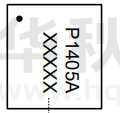
P1405A
Over voltage protector
Description
The P1405A over-voltage protection device features an ultra-low 30mΩ (typical) on-resistance high current integrated
N-MOSFET which actively protects low-voltage systems from voltage supply faults up to +32VDC. An input voltage
exceeding the over-voltage threshold will cause the internal MOSFET to turn off, preventing excessive voltage from
damaging downstream devices. P1405A has thermal protection at 140°C
The P1405A is available in a RoHS and Green compliant DFN2x2-6L package.
VIN
VBUS
VOUT
VBUSOUT
1uF
PUDN
1uF
P1405A
GND
Figure 1. Typical Application
6
1
VBUSOUT
2
PUND
3
GND
P1405X
XXXXX
YYMM
VBUS
VBUS
NC5
5
NC4
4
GND
P1405A
Figure 2. Pin order (Bottom view) and Marking (Top view)
Feature
Application
Wide Input voltage range: 3.0-32V
Cellular Phones, Smart Phones, PDAs
Ultra-low 30mohm On-resistance.
Tablet, Portable Media Players
Fixed OVP Threshold:6.0V
Gaming Device, Digital Cameras
Fast turn-off response time: 50ns
Soft-start function to avoid in-rush current
-40-85°C operation temperature
DFN2x2-6L
Rev.06.7
1
www.prisemi.com
�P1405A
Over voltage protector
Pin Definitions
Pin#
PIN Name
Description
1
VBUSOUT
2
PUND
3
GND
Ground.
4
NC4
Not connected.
5
NC5
Not connected.
6
VBUS
Output voltage.
Pull down output voltage to ground when input voltage is higher than OVP threshold
voltage.
Input voltage.
Block Diagram
VBUS,6
VBUSOUT,1
PUDN,2
OVP
Charge
control
Pump
LDO
Figure 3. IC Block Diagram
Rev.06.7
2
www.prisemi.com
�P1405A
Over voltage protector
Absolute maximum rating
Parameter(Note1)
Symbol
Value
Units
VBUS
-0.3 to 32
V
VBUSOUT
-0.3 to 7
V
PUDN voltage range
VPUDN
-0.3 to 7
V
AVDD voltage range
VAVDD
-0.3 to 7
V
Switch I/O Continuous Current
IIN
3
A
Junction temperature
TJ
150
℃
Lead temperature(Soldering,10s)
TL
260
℃
TSTG
-55 to 150
℃
3000
V
500
V
VBUS voltage range
VBUSOUT voltage range
Storage temperature
HBM
(Except VBUSOUT PIN)
ESD Ratings
CDM
Note 1: Stresses greater than those listed under "Absolute Maximum Ratings" may cause permanent damage to the device.
These are stress ratings only, and functional operation of the device at these or any other conditions beyond those indicated
under "Recommended Operating Conditions" is not implied. Exposure to "Absolute Maximum Ratings" for extended periods
may affect device reliability.
Recommended Operating Conditions
Parameter
Symbol
Value
Units
VBUS
3.0 to 32,typical=5
V
TA
-40 to 85
℃
RθJA
67.5
℃/W
VBUS input voltage range
Operating ambient temperature
Thermal Resistance
Note 2: Junction to Ambient thermal resistance is highly dependent on PCB layout. Values are based on thermal properties
of the device when soldered to an EV board.
Rev.06.7
3
www.prisemi.com
�P1405A
Over voltage protector
Electrical Characteristics
(TA=25℃,VBUS=5V,CIN=1uF,COUT=1uF,for 5V application,unless otherwise specified.)
Parameter
Symbol
Conditions
Min.
Typ.
Max.
Units
Basic Operation
IDDQ1
VBUS=5V,No load
120
uA
IDDQ2
VBUS=30V,No load
190
uA
VBUS Rising
2.4
VBUS=0->5V to Output ON
18
VBUS=5V,IOUT=1A
30
40
mΩ
6.0
6.15
V
Quiescent Supply Current
UVLO Threshold Voltage
Start-up Delay Time
Main Switch ON-Resistance
VUVLO
TSTART_DLY
RON
3.2
V
ms
Over-Voltage Protection
VBUS OVP Threshold
VOVP
OVP Response Time
tOVP
OVP Recovery Time
tR_OVP
Output discharge resistance
RDCHG
VBUS Rising
VIN >
VOVP to VOUT
stop rising
VIN <
VOVP to VOUT
start rising
VIN >
VOVP
5.85
50
ns
18
ms
400
Ω
Thermal Protection
Over-Temperature Protection Threshold
TSD
140
℃
Over-Temperature Protection Hysteresis
THYS
20
℃
Rev.06.7
4
www.prisemi.com
�P1405A
Over voltage protector
Typical Characteristics
VBUS
VBUS
VBUSOUT
VBUSOUT
IOUT
5ms/div
2ms/div
Figure 4. Start-up waveform(Rload=10Ω)
Figure 5. OVP response
VBUS
VBUSOUT
5ms/div
Figure 6. OVP recovery waveform
Rev.06.7
5
www.prisemi.com
�P1405A
Over voltage protector
Product dimension (DFN2x2-6L)
A
Millimeters
C
4
Inches
Dim
5
6
MIN
MAX
MIN
MAX
A
1.924
2.076
0.076
0.082
B
1.924
2.076
0.076
0.082
C
0.250
0.400
0.010
0.016
H
F
E
6
3
B
3
G
1
2
D
Bottom view
L
D
0.650(typ.)
0.026(typ.)
E
0.200 MIN.
0.008 MIN.
F
0.520
0.720
0.020
0.028
G
0.750
1.100
0.030
0.043
H
0.174
0.380
0.007
0.015
J
0.550
0.800
0.022
0.031
L
0
0.050
0
0.002
K
0.180
0.200
0.007
0.008
K
J
Side view
2.30
0.40
0.45
0.25
0.65
0.77
1.15
Unit:mm
PCB Layout Guide
Rev.06.7
6
www.prisemi.com
�P1405A
Over voltage protector
IMPORTANT NOTICE
and
are registered trademarks of Prisemi Electronics Co., Ltd (Prisemi) ,Prisemi
reserves the right to make changes without further notice to any products herein. Prisemi makes
no warranty, representation or guarantee regarding the suitability of its products for any particular
purpose, nor does Prisemi
assume any liability arising out of the application or use of any
product or circuit, and specifically disclaims any and all liability, including without limitation
special, consequential or incidental damages. “Typical” parameters which may be provided in
Prisemi data sheets and/or specifications can and do vary in different applications and actual
performance may vary over time. All operating parameters, including “Typicals” must be
validated for each customer application by customer’s technical experts. Prisemi does not
convey any license under its patent rights nor the rights of others. The products listed in this
document are designed to be used with ordinary electronic equipment or devices, Should you
intend to use these products with equipment or devices which require an extremely high level of
reliability and the malfunction of with would directly endanger human life (such as medical
instruments, aerospace machinery, nuclear-reactor controllers, fuel controllers and other safety
devices), please be sure to consult with our sales representative in advance.
Website: http://www.prisemi.com
For additional information, please contact your local Sales Representative.
©Copyright 2009, Prisemi Electronics
is a registered trademark of Prisemi Electronics.
All rights are reserved.
Rev.06.7
7
www.prisemi.com
�
很抱歉,暂时无法提供与“P1405A”相匹配的价格&库存,您可以联系我们找货
免费人工找货