PYu-RE_105_RoH
S_P_1.doc
DATA SHEET
THICK FILM LEAD FREE CHIP RESISTORS
Precision grade
RE_P series
0.1%, 0.5%, 1%, TC 50 & 100
Product specification – June 06, 2023 V.3
sizes 0201/0402/0603/0805/1206
�Product specification
Chip Resistor Surface Mount
RE_P
SCOPE
ORDERING INFORMATION - GLOBAL PART NUMBER
This specification describes
RE0201 to RE1206 ultra precision
chip resistors made by thick film
process.
Both part numbers are identified by the series, size, tolerance, packing
type, temperature coefficient, taping reel and resistance value.
APPLICATIONS
RE XXXX X X X XX XXXX P
Total lead free without RoHS
exemption
Converters
Printer equipment
Server board
Telecom
Consumer
FEATURES
Halogen Free Epoxy
Reducing environmentally
hazardous wastes
High component and equipment
reliability
Non-forbidden material used in
products/production
Moisture sensitivity level: MSL 1
2
8
0201 to 1206
SERIES
YAGEO BRAND ordering code
GLOBAL PART NUMBER (PREFERRED )
(1)
(2) (3) (4)
(5)
(6)
(7)
(1) SIZE
0201 / 0402 / 0603 / 0805 / 1206
(2) TOLERANCE
B = ± 0.1%
D = ± 0.5%
F = ± 1%
(3) PACKAGING TYPE
R = Paper/PE taping reel
(4) TEMPERATURE COEFFICIENT OF RESISTANCE
E = ± 50 ppm/°C
F = ± 100 ppm/°C
(5) TAPING REEL
07 = 7 inch dia. Reel
10 = 10 inch dia. Reel
13 = 13 inch dia. Reel
(6) RESISTANCE VALUE
There are 2~4 digits indicated the resistor value. Letter R/K/M is decimal point, no need
to mention the last zero after R/K/M, e.g.1K2, not 1K20.
Detailed resistance rules show in table of “Resistance rule of global part number”.
(7) DEFAULT CODE
Letter P is lead free (without RoHS exemption)
Resistance rule of global part
number
Resistance code rule
Example
XXRX
(10 to 97.6 Ω)
10R = 10 Ω
97R6 = 97.6 Ω
XXXR
(100 to 976 Ω)
100R = 100 Ω
XKXX
(1 to 9.76 KΩ)
1K = 1,000 Ω
9K76 = 9760 Ω
XMXX
(1 MΩ)
O RDERING EXAMPLE
The ordering code of a RE0603
chip resistor, TC 50 value 56 with
±0.5% tolerance, supplied in 7-inch
tape reel is: RE0603DRE0756RP.
1M = 1,000,000 Ω
www.yageo.com
Jun. 06, 2023 V.3
�Product specification
Chip Resistor Surface Mount
RE_P
3
8
0201 to 1206
SERIES
MARKING
RE0805 / RE1206
00
Either resistance in E-24 or E-96: 4 digits
YNSC004
Fig. 1 Value = 10 kΩ
First three digits for significant figure and 4th digit for number of zeros
RE0603
0
1%, 0.5%, 0.1% E24 exception values 10/11/13/15/20/75 of E24 series
YNSC037
Fig. 2 Value = 24 Ω
1%, 0.5%, 0.1% E96 refer to EIA-96 marking method, including values
Fig. 3 Value = 12.4 kΩ
10/11/13/15/20/75 of E24 series
RE0201/0402
No marking
ynsc007
Fig. 4
For further marking information, please see special data sheet “Chip resistors marking”.
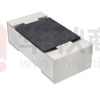
CONSTRUCTION
OUTLINES
The resistors are constructed out of a high-grade ceramic
body. Internal metal electrodes are added at each end and
connected by a resistive layer. The resistive layer is adjusted
to give the approximate required resistance and laser cutting
of this resistive layer that achieves tolerance trims the value.
The resistive layer is covered with a protective coat and
printed with the resistance value. Finally, the two external
terminations (matte tin) are added. See fig. 5.
For dimension see Table 1
DIMENSION
Table 1 For outlines see fig. 5
TYPE
L (mm) W (mm) H (mm)
I1 (mm)
I2 (mm)
RE0201 0.60 ± 0.03 0.30 ± 0.03 0.23 ± 0.03 0.10 ± 0.05 0.15 ± 0.05
RE0402 1.00 ± 0.05 0.50 ± 0.05 0.32 ± 0.05 0.20 ± 0.10 0.25 ± 0.10
RE0603 1.60 ± 0.10 0.80 ± 0.10 0.45 ± 0.10 0.25 ± 0.15 0.25 ± 0.15
RE0805 2.00 ± 0.10 1.25 ± 0.10 0.50 ± 0.10 0.35 ± 0.20 0.35 ± 0.20
RE1206 3.10 ± 0.10 1.60 ± 0.10 0.55 ± 0.10 0.45 ± 0.20 0.45 ± 0.20
Fig. 5 Chip resistor outlines
www.yageo.com
Jun. 06, 2023 V.3
�Product specification
Chip Resistor Surface Mount
RE_P
SERIES
4
8
0201 to 1206
ELECTRICAL CHARACTERISTICS
Table 2
RESISTANCE
RANGE
TYPE
(E24/E96)
OPERATING
TEMPERATURE RANGE
MAXIMUM
WORKING
RATING VOLTAGE
POWER
DIELECTRIC
WITHSTAND
VOLTAGE
MAXIMUM
OVERLOAD
VOLTAGE
RE0201
100 Ω to 2 MΩ
–55 °C to +155 °C
1/20W
25 V
50 V
50 V
RE0402
10 Ω to 10 MΩ
–55 °C to +155 °C
1/16 W
50 V
100 V
100 V
RE0603
10 Ω to 10 MΩ
–55 °C to +155 °C
1/10 W
75 V
150 V
150 V
RE0805
10 Ω to 10 MΩ
–55 °C to +155 °C
1/8 W
150 V
300 V
300 V
RE1206
10 Ω to 10 MΩ
–55 °C to +155 °C
1/4 W
200 V
500 V
400 V
TEMPERATURE
COEFFICIENT OF
RESISTANCE
± 50 ppm/°C
± 100 ppm/°C
± 50 ppm/°C
± 100 ppm/°C
± 50 ppm/°C
± 100 ppm/°C
± 50 ppm/°C
± 100 ppm/°C
± 50 ppm/°C
± 100 ppm/°C
NOTE
The maximum working voltage that may be continuously applied to the resistor element, see “IEC publication 60115-8”
FOOTPRINT AND SOLDERING PROFILES
For recommended footprint and soldering profiles, please see the special data sheet “Chip resistors mounting”.
PACKING STYLE AND PACKAGING QUANTITY
Table 3 Packing style and packaging quantity
PACKING STYLE
REEL DIMENSION
Paper/PE taping reel (R)
RE0201
RE0402
RE0603
RE0805
RE1206
7" (178 mm)
10,000
10,000
5,000
5,000
5,000
10" (254 mm)
20,000
20,000
10,000
10,000
10,000
13" (330 mm)
50,000
50,000
20,000
20,000
20,000
NOTE
1. For Paper/PE tape and reel specification/dimensions, please see the special data sheet “Chip resistors packing”
FUNCTIONAL DESCRIPTION
POWER RATING
Each type rated power at 70°C:
RE0201=1/20W, RE0402=1/16W, RE0603=1/10 W,
RE0805=1/8 W, RE1206=1/4W
MLB206_2
P
(%Prated )
100
50
R ATED VOLTAGE
The DC or AC (rms) continuous working voltage
corresponding to the rated power is determined by
the following formula:
V=√(P X R)
or max. working voltage whichever is less
0
55
0
50
70
100
155
o
Tamb ( C)
Fig. 6 Maximum dissipation (P) in percentage of rated power as a
function of the operating ambient temperature (T amb )
Where
V=Continuous rated DC or
AC (rms) working voltage (V)
P=Rated power (W)
R=Resistance value (Ω)
www.yageo.com
Jun. 06, 2023 V.3
�Product specification
Chip Resistor Surface Mount
RE_P
SERIES
5
8
0201 to 1206
TESTS AND REQUIREMENTS
Table 4 Test condition, procedure and requirements
TEST
TEST METHOD
PROCEDURE
REQUIREMENTS
Life/Endurance
IEC 60115-1 7.1
± (3%+0.05 Ω)
MIL-STD-202 Method 108
At 70± 2 °C for 1,000 hours, RCWV applied for
1.5 hours on, 0.5 hour off, still air required
High
Temperature
Exposure
IEC 60068-2-2
1,000 hours at 155± 5 °C, unpowered
± (3%+0.05 Ω)
Moisture
Resistance
MIL-STD-202 Method 106
Each temperature / humidity cycle is defined at 8
hours, 3 cycles / 24 hours for 10d. with 25 °C /
65 °C 95% R.H, without steps 7a & 7b,
unpowered
± (3%+0.05 Ω)
MIL-STD-202 Method 108
Parts mounted on test-boards, without
condensation on parts
Measurement at 24± 2 hours after
test conclusion
Thermal Shock
MIL-STD-202 Method 107
-55/+125 °C
Number of cycles required is 300.
± (1%+0.05 Ω)
Devices mounted
Maximum transfer time is 20 seconds. Dwell time
is 15 minutes. Air – Air
Short Time
Overload
IEC60115-1 8.1
Board Flex/
Bending
IEC 60115-1 9.8
2.5 times of rated voltage or maximum overload
voltage whichever is less for 5 sec at room
temperature
± (1%+0.05 Ω)
Chips mounted on a 100mm x 40mm glass epoxy
resin PCB (FR4)
± (1%+0.05 Ω)
No visible damage
No visible damage
Bending: see table 5 for each size
Bending time: 60± 5 seconds
www.yageo.com
Jun. 06, 2023 V.3
�Product specification
Chip Resistor Surface Mount
RE_P
SERIES
6
8
0201 to 1206
TEST
TEST METHOD
PROCEDURE
REQUIREMENTS
Humidity
IEC 60115-1 10.4
Steady state for 1000 hours at 40 °C / 95%
R.H. RCWV applied for 1.5 hours on and 0.5
hour off
± (3%+0.05 Ω)
Solderability
- Wetting
J-STD-002 test B1
Electrical Test not required
Magnification 50X
SMD conditions:
1st step: aging 4 hours at 155°C dry heat
2nd step: method B1, leadfree solder bath at
245± 3°C
Dipping time: 3± 0.5 seconds
Well tinned (≥95% covered)
No visible damage
- Leaching
J-STD-002 test D
Leadfree solder, 260 °C, 30 seconds
immersion time
No visible damage
IEC 60115-1 4.18
Condition B, no pre-heat of samples.
Leadfree solder, 260 °C, 10 seconds
immersion time
Procedure 2 for SMD: devices fluxed and
cleaned with isopropanol
± (1%+0.05 Ω)
- Resistance to
Soldering Heat
No visible damage
Table 5 Bending for sizes 0201 to 1206
TYPE
Specification (mm)
RE0201
RE0402
RE0603
RE0805
RE1206
5
5
3
3
2
www.yageo.com
Jun. 06, 2023 V.3
�Product specification
Chip Resistor Surface Mount
RE_P
SERIES
0201 to 1206
7
8
REVISION HISTORY
REVISION DATE
CHANGE NOTIFICATION
DESCRIPTION
Version 3
Jun. 06, 2023
-
- Range of 0402~1206 upgrade to 10Mohm
Version 2
Oct. 29, 2021
-
- Add TCR ± 100 ppm/°C
Version 1
Oct. 15, 2021
-
- Range of 0201 upgrade to 2Mohm
Version 0
Mar. 13, 2021
-
- First issue of this specification
www.yageo.com
Jun. 06, 2023 V.3
�Product specification
Chip Resistor Surface Mount
RE_P
SERIES
8
8
0201 to 1206
LEGAL DISCLAIMER
YAGEO, its distributors and agents (collectively, “YAGEO”), hereby disclaims any and all liabilities for any
errors, inaccuracies or incompleteness contained in any product related information, including but not limited
to product specifications, datasheets, pictures and/or graphics. YAGEO may make changes, modifications and/or
improvements to product related information at any time and without notice.
YAGEO makes no representation, warranty, and/or guarantee about the fitness of its products for any
particular purpose or the continuing production of any of its products. To the maximum extent permitted by
law, YAGEO disclaims (i) any and all liability arising out of the application or use of any YAGEO product, (ii)
any and all liability, including without limitation special, consequential or inciden tal damages, and (iii) any and all
implied warranties, including warranties of fitness for a particular purpose, non -infringement and
merchantability.
YAGEO products are designed for general purpose applications under normal operation and usage conditio ns.
Please contact YAGEO for the applications listed below which require especially high reliability for the
prevention of defects which might directly cause damage to the third party's life, body or property: Aerospace
equipment (artificial satellite, rocket, etc.), Atomic energy-related equipment, Aviation equipment, Disaster
prevention equipment, crime prevention equipment, Electric heating apparatus, burning equipment, Highly
public information network equipment, data-processing equipment , Medical devices, Military equipment, Power
generation control equipment, Safety equipment, Traffic signal equipment, Transportation equipment and
Undersea equipment, or for any other application or use in which the failure of YAGEO products could result
in personal injury or death, or serious property damage. Particularly YAGEO Corporation and its affiliates
do not recommend the use of commercial or automotive grade products for high reliability
applications or manned space flight.
Information provided here is intended to indicate product specifications only. YAGEO reserves all the rights
for revising this content without further notification, as long as products are unchanged. Any product change
will be announced by PCN.
www.yageo.com
Jun. 06, 2023 V.3
�


 工商网监
湘ICP备2023018690号
工商网监
湘ICP备2023018690号
