芯
洲
科
SCT2A26
技
Silicon Content Technology
Rev.1.0
5.5V-100V Vin, 4A Peak Current Limit, High Efficiency Asynchronous
Step-down DCDC Converter
FEATURES
DESCRIPTION
The SCT2A26 is an asynchronous buck converter with
wide input voltage ranging from 5.5V to 100V which
accommodates a variety of step-down applications,
making it ideal for automotive, industry, and lighting
applications. The SCT2A26 integrates an 500mΩ highside MOSFET and has 4A peak output current limit to
support high peak current application in GPS tracker
with 4G Module.
Wide Input Range: 5.5V-100V
Maximum Output Voltage: 30V
2A Continuous Output Current
4A Peak Current Limit
Integrated 500mΩ High-Side Power MOSFET
140uA Quiescent Current
1.2V ±1% Feedback Reference Voltage
4ms Internal Soft-start Time
Fixed Switching Frequency at 300KHz
COT Control Mode with Integrated Loop
Compensation
Precision Enable Threshold for Programmable
Input Voltage Under-voltage Lock Out Protection
(UVLO) Threshold and Hysteresis
Cycle-by-Cycle Current Limiting
Over-Voltage Protection
Over-Temperature Protection
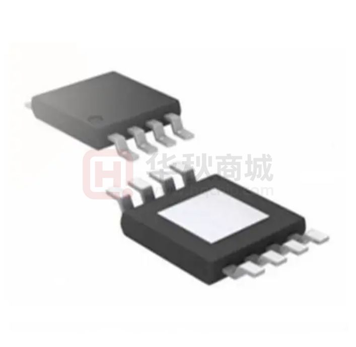
Available in an ESOP-8 Package
APPLICATIONS
The SCT2A26, adopting the constant-on time (COT)
mode control with integrated loop compensation
greatly simplifies the converter off-chip configuration.
The SCT2A26 features Pulse Frequency Modulation
(PFM) mode at light load with typical 140uA low
quiescent current, which enables the converter to
achieve the high-power efficiency during light-load or
no-load conditions.
The SCT2A26 offers cycle-by-cycle current limit,
thermal shutdown protection, output over-voltage
protection and input voltage under-voltage protection.
The device is available in an 8-pin thermally enhanced
SOP-8 package.
GPS Tracker
E-bike, Scooter
Moto Drives, Drones
48V Industry Power Bus System
TYPICAL APPLICATION
100
GND
90
SW
80
VIN
BST
Efficiency(%)
VIN
SCT2A26
ON/OFF
EN
NC
TM
FB
70
60
50
24VIN 12VOUT
40
36VIN 12VOUT
30
48VIN 12VOUT
20
60VIN 12VOUT
10
0
0.001
72VIN 12VOUT
0.01
Iout(A)
0.1
1
Efficiency, Vout=12V
For more information www.silicontent.com
© 2022 Silicon Content Technology Co., Ltd. All Rights Reserved
Product Folder Links: SCT2A26
1
�SCT2A26
REVISION HISTORY
NOTE: Page numbers for previous revisions may differ from page numbers in the current version.
Revision 0.8: Sampling
DEVICE ORDER INFORMATION
PART NUMBER
PACKAGE MARKING
PACKAGE DISCRIPTION
SCT2A26STE
2A26
8-Lead Plastic ESOP
1)For Tape & Reel, Add Suffix R (e.g. SCT2A26STER).
ABSOLUTE MAXIMUM RATINGS
PIN CONFIGURATION
Over operating free-air temperature unless otherwise
DESCRIPTION
MIN
noted(1)
MAX
UNIT
VIN
-0.3
110
V
BST
-0.3
116
V
SW
-1
110
V
BST-SW
-0.3
6
V
EN, FB, TM
-0.3
6
V
Operating junction temperature TJ(2)
-40
150
°C
Storage temperature TSTG
-65
150
°C
(1)
(2)
GND
1
VIN
2
EN
3
NC
4
Thermal
PAD
9
8
SW
7
BST
6
TM
5
FB
Figure 1. 8-Lead Plastic E-SOP
Stresses beyond those listed under Absolute Maximum Rating may cause device permanent damage. The device is not guaranteed to
function outside of its Recommended Operation Conditions.
The IC includes over temperature protection to protect the device during overload conditions. Junction temperature will exceed 150°C
when over temperature protection is active. Continuous operation above the specified maximum operating junction temperature will
reduce lifetime.
PIN FUNCTIONS
NAME
NO.
GND
1
VIN
2
EN
3
NC
2
FB
5
TM
6
BST
7
SW
8
Thermal Pad
9
2
PIN FUNCTION
Ground
Input supply voltage. Connect a local bypass capacitor from VIN pin to GND pin. Path
from VIN pin to high frequency bypass capacitor and GND must be as short as possible.
Enable pin to the regulator with internal pull-up current source. Pull below 1.23V to
disable the converter. Floating to enable the converter.
Not Connection.
Inverting input of the comparator. The tap of external feedback resistor divider from the
output to GND sets the output voltage. The device regulates FB voltage to the internal
reference value of 1.2V typical.
Test mode pin for factory use only. Connect TM to EN pin, ground or leave floating.
Power supply bias for high-side power MOSFET gate driver. Connect a 0.1uF capacitor
from BOOT pin to SW pin. Bootstrap capacitor is charged when low-side power
MOSFET is on or SW voltage is low.
Regulator switching output. Connect SW to an external power inductor
Heat dissipation path of die. Electrically connection to GND pin. Must be connected to
ground plane on PCB for proper operation and optimized thermal performance.
For more information www.silicontent.com
© 2022 Silicon Content Technology Co., Ltd. All Rights Reserved
Product Folder Links: SCT2A26
�SCT2A26
RECOMMENDED OPERATING CONDITIONS
Over operating free-air temperature range unless otherwise noted
PARAMETER
DEFINITION
VIN
VOUT
TJ
Input voltage range
Output voltage range
Operating junction temperature
MIN
MAX
UNIT
5.5
1.2
-40
100
30
150
V
V
°C
MIN
MAX
UNIT
-1
+1
kV
-1
+1
kV
ESD RATINGS
PARAMETER
VESD
DEFINITION
Human Body Model(HBM), per ANSI-JEDEC-JS-001-2014
specification, all pins(1)
Charged Device Model(CDM), per ANSI-JEDEC-JS-0022014 specification, all pins(2)
(1) JEDEC document JEP155 states that 500V HBM allows safe manufacturing with a standard ESD control process.
(2) JEDEC document JEP157 states that 250V CDM allows safe manufacturing with a standard ESD control process.
THERMAL INFORMATION
PARAMETER
RθJA
RθJC
THERMAL METRIC
Junction to ambient thermal resistance(1)
Junction to case thermal
resistance(1)
ESOP-8L
42
45.8
UNIT
°C/W
(1) SCT provides RθJA and RθJC numbers only as reference to estimate junction temperatures of the devices. RθJA and RθJC are not a
characteristic of package itself, but of many other system level characteristics such as the design and layout of the printed circuit
board (PCB) on which the SCT2A26 is mounted, thermal pad size, and external environmental factors. The PCB board is a heat sink
that is soldered to the leads and thermal pad of the SCT2A26. Changing the design or configuration of the PCB board changes the
efficiency of the heat sink and therefore the actual RθJA and RθJC.
For more information www.silicontent.com
© 2022 Silicon Content Technology Co., Ltd. All Rights Reserved
Product Folder Links: SCT2A26
3
�SCT2A26
ELECTRICAL CHARACTERISTICS
VIN=48V, TJ=-40°C~125°C, typical value is tested under 25°C.
SYMBOL
PARAMETER
TEST CONDITION
Power Supply
VIN
Operating input voltage
VIN rising
Hysteresis
Shutdown current from VIN
pin
Quiescent current from VIN
pin
ISHDN
IQ
TYP
5.5
VIN UVLO Threshold
VUVLO
MIN
Power MOSFETs
High-side MOSFET onRDSON_H
resistance
4.7
5
MAX
UNIT
100
V
5.3
V
440
mV
EN=0, no load
4.2
10
μA
EN floating, no load, non- switching,
BOOT-SW=5V
140
240
μA
VBOOT-VSW=5V
500
950
mΩ
1.2
1.212
Reference and Control Loop
VREF
Reference voltage of FB
1.188
Enable and Soft-startup
VEN_H
Enable high threshold
V
1.25
V
IEN_L
Enable pin pull-up current
EN=0V
0.3
uA
IEN_H
Enable pin pull-up current
Enable pin pull-up current
hysteresis
Internal soft start time
EN=1.5V
2.1
μA
1.8
uA
4
ms
IEN_Hys
Tss
Switching Frequency Timing
FSW
Switching frequency
TOFF_MIN
Minimum off-time
260
300
340
kHz
200
260
ns
A
Current Limit and Over Current Protection
ILIM
HS MOSFET current limit
TJ=25°C
3.5
4
4.5
TJ=-40°C~125°C
3.3
4
4.7
Protection
VOVP
TSD
Feedback overvoltage with
respect to
reference voltage
Thermal shutdown threshold*
VFB/VREF rising
120
%
VFB/VREF falling
TJ rising
Hysteresis
115
160
23
%
°C
°C
*Derived from bench characterization
4
For more information www.silicontent.com
© 2022 Silicon Content Technology Co., Ltd. All Rights Reserved
Product Folder Links: SCT2A26
�SCT2A26
100
100
90
90
80
80
70
70
Efficiency(%)
Efficiency(%)
TYPICAL CHARACTERISTICS
60
50
24VIN 12VOUT
40
36VIN 12VOUT
30
48VIN 12VOUT
20
60VIN 12VOUT
10
0.01
Iout(A)
0.1
12VIN 5VOUT
40
24VIN 5VOUT
30
36VIN 5VOUT
20
48VIN 5VOUT
60VIN 5VOUT
1
5
4.99
12.06
4.98
12.04
4.97
12.02
4.96
Vout(V)
12.1
12
11.98
VIN=24V
1
4.95
4.94
VIN=24V
VIN=36V
VIN=48V
4.91
VIN=60V
11.9
0.1
4.92
VIN=48V
11.92
Iout(A)
4.93
VIN=36V
11.94
0.01
Figure 3. Efficiency vs Load Current, Vout=5V
12.08
11.96
72VIN 5VOUT
0
0.001
Figure 2. Efficiency vs Load Current, Vout=12V
Vout(V)
50
10
72VIN 12VOUT
0
0.001
60
VIN=60V
4.9
0
0.5
1
1.5
2
0
0.5
Iout(A)
1
1.5
2
Iout(A)
Figure 4. Load Regulation, Vout=12V
Figure 5. Load Regulation, Vout=5V
12.07
330
325
12.05
320
Fsw(KHz)
Vout(V)
12.03
12.01
11.99
315
310
305
300
295
290
11.97
285
11.95
280
10
20
30
40
50
60
70
80
90
100
20
Vin(V)
40
60
80
100
Vin(V)
Figure 6. Line Regulation, Vout=12V
Figure 7. Switching Frequency vs Vin, Vout=5V
For more information www.silicontent.com
© 2022 Silicon Content Technology Co., Ltd. All Rights Reserved
Product Folder Links: SCT2A26
5
�SCT2A26
FUNCTIONAL BLOCK DIAGRAM
VIN
0.3uA
2.1uA
Thermal
Shutdown
+
EN
EN LOGIC
VIN UVLO
Reference
1.25V
VREF
VCC
Boot
Charge
Current Limit
and Off Timer
Soft-start
Timer
BST
DC Error
Correction
1.2V
Boot
UVLO
PWM
+
+
FB
Q1
Ramp
Compensation
+
Control
Logic
SW
OVP
120%VREF
VCC
On-Time
Generator
TM
GND
Figure 8. Functional Block Diagram
6
For more information www.silicontent.com
© 2022 Silicon Content Technology Co., Ltd. All Rights Reserved
Product Folder Links: SCT2A26
�SCT2A26
OPERATION
Overview
The SCT2A26 is a 5.5V-100V input, 4A peak current limit, Step-down DCDC converter with built-in 500mΩ highside power MOSFET. It implements constant on time control to regulate output voltage, providing excellent line and
load transient response, and internal error amplifier integrated improve the line and load regulation.
The SCT2A26 features an internal 4ms soft-start time to avoid large inrush current and output voltage overshoot
during startup. The switching frequency is fixed at 300KHz. The device also supports monolithic startup with prebiased output condition.
The SCT2A26 has a default input start-up voltage of 5V with 440mV hysteresis. The EN pin has a precision
threshold that can be used to adjust the input voltage lockout thresholds with two external resistors to meet accurate
higher UVLO system requirements. Floating EN pin enables the device with the internal pull-up current to the pin.
The SCT2A26 full protection features include the VIN input under-voltage lockout, the output over-voltage protection,
over current protection with cycle-by-cycle current limit, output hard short protection and thermal shutdown
protection.
Constant On-Time Mode Control
The SCT2A26 employs constant on-time (COT) Mode control providing fast transient with pseudo fixed switching
frequency. At the beginning of each switching cycle, since the feedback voltage (VFB) is lower than the internal
reference voltage (VREF), the high-side MOSFET (Q1) is turned on during one on-time and the inductor current
rises to charge up the output voltage. The on-time is determined by the input voltage and output voltage. After the
on-time, the high-side MOSFET (Q1) turns off. The inductor current drops and the output capacitors are discharged.
When the output voltage decreases and the VFB decreased below the VREF or SS, the Q1 turns on again after
another dead time duration. This repeats on cycle-by-cycle.
The SCT2A26 works with an internal compensation, so customer could use the device easily. Feedforward cap Cf
is necessary to provide flexibility for optimizing the loop stability and transient response.
Enable and Under Voltage Lockout Threshold
The SCT2A26 is enabled when the VIN pin voltage rises above 5V and the EN pin voltage exceeds the enable
threshold of 1.24V. The device is disabled when the VIN pin voltage falls below 4.56V or when the EN pin voltage
is below 1.23V. Internal pull up current source to EN pin allows the device enable when EN pin floats.
For a higher system UVLO threshold, connect an external resistor divider (R3 and R4) shown in Figure 9 from VIN
to EN. The UVLO rising and falling threshold can be calculated by Equation 1 and Equation 2 respectively.
𝑉𝐼𝑁𝑟𝑖𝑠𝑒 = 𝑉𝐸𝑁_𝐻 ∗
𝑅3 + 𝑅4
𝑅4
(1)
VIN
I2
2.1 uA
I1
0.3uA
(2)
𝑉𝐼𝑁_ℎ𝑦𝑠 = 𝐼2 ∗ 𝑅3
R3
Where
EN
VIN_rise: Vin rise threshold to enable the device
VIN_hys: Vin hysteresis threshold
+
EN
1.25V
R4
I2=2.1uA
VEN_H=1.25V
Figure 9. System UVLO by enable divide
For more information www.silicontent.com
© 2022 Silicon Content Technology Co., Ltd. All Rights Reserved
Product Folder Links: SCT2A26
7
�SCT2A26
Output Voltage
The SCT2A26 regulates the internal reference voltage at 1.2V with 1% tolerance over the operating temperature
and voltage range. The output voltage is set by a resistor divider from the output node to the FB pin. It is
recommended to use 1% tolerance or better resistors. Use Equation 3 to calculate resistance of resistor dividers.
To improve efficiency at light loads, larger value resistors are recommended. However, if the values are too high,
the regulator will be more susceptible to noise affecting output voltage accuracy.
𝑉𝑂𝑈𝑇
𝑅𝐹𝐵_𝑇𝑂𝑃 = (
− 1) ∗ 𝑅𝐹𝐵_𝐵𝑂𝑇
𝑉𝑅𝐸𝐹
(3)
where
RFB_TOP is the resistor connecting the output to the FB pin.
RFB_BOT is the resistor connecting the FB pin to the ground.
Internal Soft-Start
The SCT2A26 integrates an internal soft-start circuit that ramps the reference voltage from zero volts to 1.2V
reference voltage in 4ms. If the EN pin is pulled below 1.23V, switching stops and the internal soft-start resets.
The soft-start also resets during shutdown due to thermal overloading.
Bootstrap Voltage Regulator
An external bootstrap capacitor between BOOT pin and SW pin powers the floating gate driver to high-side power
MOSFET. The bootstrap capacitor voltage is charged from an integrated voltage regulator when high-side power
MOSFET is off and low-side power MOSFET is on.
The UVLO of high-side MOSFET gate driver has rising threshold of 2.95V and hysteresis of 250mV. When the
device operates with high duty cycle or extremely light load, bootstrap capacitor may be not recharged in
considerable long time. The voltage at bootstrap capacitor is insufficient to drive high-side MOSFET fully on. When
the voltage across bootstrap capacitor drops below 2.7V, BOOT UVLO occurs. The converter forces turning on an
integrated low-side MOSFET periodically to refresh the voltage of bootstrap capacitor to guarantee the converter’s
operation over a wide duty range.
Over Current Limit
The inductor current is monitored during high-side FET turn on. The SCT2A26 implements over current protection
with cycle-by-cycle limiting high-side MOSFET peak current during unexpected overload or output hard short.
SCT2A26 also provide a HS current limit off timer for making the IC safer when trigger over current condition. Once
trigger HS over current, the present on-time period is immediately terminated to avoid the inductor current run away.
The length of off time is controlled by FB voltage and VIN voltage and could be calculated by the following equation.
𝑉𝐼𝑁
𝑇𝑜𝑓𝑓 = 1.5 ∗ (
) 𝑢𝑠
20 ∗ 𝑉𝐹𝐵 + 4.35
(4)
Over voltage Protection
The SCT2A26 implements the Over-voltage Protection OVP circuitry to minimize output voltage overshoot during
load transient, recovering from output fault condition or light load transient. The overvoltage comparator in OVP
circuit compares the FB pin voltage to the internal reference voltage. When FB voltage exceeds 120% of internal
1.2V reference voltage, the high-side MOSFET turns off to avoid output voltage continue to increase. When the FB
pin voltage falls below 115% of the 1.2V reference voltage, the high-side MOSFET can turn on again.
Thermal Shutdown
The SCT2A26 protects the device from the damage during excessive heat and power dissipation conditions. Once
the junction temperature exceeds 160°C, the internal thermal sensor stops power MOSFETs switching. When the
junction temperature falls below 137°C, the device restarts with internal soft start phase.
8
For more information www.silicontent.com
© 2022 Silicon Content Technology Co., Ltd. All Rights Reserved
Product Folder Links: SCT2A26
�SCT2A26
APPLICATION INFORMATION
Typical application
L1 68uH
VOUT=12V IOUT= 2A
GND
C1
10uF
SW
C2
0.1uF
C3
0.1uF
VIN
VIN=5.5~100V
D1
100V/5A
BST
C4
44uF
R2
271K
C5
150pF
SCT2A26
ON/OFF
EN
TM
NC
FB
R3
5K
R1
30K
Figure 10. SCT2A26 Design Example, 12V Output with Programmable UVLO
Design Parameters
Design Parameters
Example Value
Input Voltage
48V Normal, 24V to 100V
Output Voltage
12V
Maximum Output Current
2A
Switching Frequency
300 KHz
Output voltage ripple (peak to peak)
15mV
Transient Response 0.2A to 1.8A load step
∆Vout = 100mV
Transient Response 0.75A to 1.25A load step
∆Vout = 50mV
For more information www.silicontent.com
© 2022 Silicon Content Technology Co., Ltd. All Rights Reserved
Product Folder Links: SCT2A26
9
�SCT2A26
Output Voltage
The output voltage is set by an external resistor divider
R1 and R2 in typical application schematic.
Recommended R1 resistance is 30KΩ. Use equation 5
to calculate R2.
𝑉𝑂𝑈𝑇
𝑅2 = (
− 1) ∗ 𝑅1
𝑉𝑅𝐸𝐹
where:
Table 1. R1, R2Value for Common Output Voltage
(Room Temperature)
(5)
VOUT
R2
R1
5 V
95 KΩ
30 KΩ
12 V
271 KΩ
30 KΩ
24V
191 KΩ
10 KΩ
VREF is the feedback reference voltage of 1.2V
Under Voltage Lock-Out
An external voltage divider network of R3 from the input to EN pin and R4 from EN pin to the ground can set the
input voltage’s Under Voltage Lock-Out (UVLO) threshold. The UVLO has two thresholds, one for power up when
the input voltage is rising and the other for power down or brown outs when the input voltage is falling. For the
example design, the supply should turn on and start switching once the input voltage increases above 15V (start or
enable). After the regulator starts switching, it should continue to do so until the input voltage falls below 14V (stop
or disable). Use Equation 6 and Equation 7 to calculate the values 464 kΩ and 42.2 kΩ of R3 and R4 resistors.
𝑉𝐼𝑁𝑟𝑖𝑠𝑒 = 𝑉𝐸𝑁_𝐻 ∗
𝑅3 + 𝑅4
𝑅4
VIN
(6)
I2
2.1uA
I1
0.3uA
(7)
𝑉𝐼𝑁_ℎ𝑦𝑠 = 𝐼2 ∗ 𝑅3
R3
Where
EN
VIN_rise: Vin rise threshold to enable the device
VIN_hys: Vin hysteresis threshold
+
EN
1.25V
R4
I2=2.1uA
VEN_H=1.25V
Figure 11. System UVLO by enable divide
Inductor Selection
There are several factors should be considered in selecting inductor such as inductance, saturation current, the
RMS current and DC resistance(DCR). Larger inductance results in less inductor current ripple and therefore leads
to lower output voltage ripple. However, the larger value inductor always corresponds to a bigger physical size,
higher series resistance, and lower saturation current. A good rule for determining the inductance to use is to allow
the inductor peak-to-peak ripple current to be approximately 20%~40% of the maximum output current.
The peak-to-peak ripple current in the inductor ILPP can be calculated as in Equation 8.
𝐼𝐿𝑃𝑃 =
10
𝑉𝑂𝑈𝑇 ∗ (𝑉𝐼𝑁 − 𝑉𝑂𝑈𝑇 )
𝑉𝐼𝑁 ∗ 𝐿 ∗ 𝑓𝑆𝑊
(8)
For more information www.silicontent.com
© 2022 Silicon Content Technology Co., Ltd. All Rights Reserved
Product Folder Links: SCT2A26
�SCT2A26
Where
ILPP is the inductor peak-to-peak current
L is the inductance of inductor
fSW is the switching frequency
VOUT is the output voltage
VIN is the input voltage
Since the inductor-current ripple increases with the input voltage, so the maximum input voltage in application is
always used to calculate the minimum inductance required. Use Equation 9 to calculate the inductance value.
𝐿𝑀𝐼𝑁 =
Where
𝑉𝑂𝑈𝑇
𝑉𝑂𝑈𝑇
∗ (1 −
)
𝑓𝑆𝑊 ∗ 𝐿𝐼𝑅 ∗ 𝐼𝑂𝑈𝑇(𝑚𝑎𝑥)
𝑉𝐼𝑁(𝑚𝑎𝑥)
(9)
LMIN is the minimum inductance required
fsw is the switching frequency
VOUT is the output voltage
VIN(max) is the maximum input voltage
IOUT(max) is the maximum DC load current
LIR is coefficient of ILPP to IOUT
The total current flowing through the inductor is the inductor ripple current plus the output current. When selecting
an inductor, choose its rated current especially the saturation current larger than its peak operation current and
RMS current also not be exceeded. Therefore, the peak switching current of inductor, ILPEAK and ILRMS can be
calculated as in equation 10 and equation 11.
𝐼𝐿𝑃𝐸𝐴𝐾 = 𝐼𝑂𝑈𝑇 +
𝐼𝐿𝑃𝑃
2
𝐼𝐿𝑅𝑀𝑆 = √(𝐼𝑂𝑈𝑇 )2 +
Where
(10)
1
∗ (𝐼𝐿𝑃𝑃 )2
12
(11)
ILPEAK is the inductor peak current
IOUT is the DC load current
ILPP is the inductor peak-to-peak current
ILRMS is the inductor RMS current
In overloading or load transient conditions, the inductor peak current can increase up to the switch current limit of
the device which is typically 4A. The most conservative approach is to choose an inductor with a saturation current
rating greater than 4A. Because of the maximum ILPEAK limited by device, the maximum output current that the
SCT2A26 can deliver also depends on the inductor current ripple. Thus, the maximum desired output current also
affects the selection of inductance. The smaller inductor results in larger inductor current ripple leading to a lower
maximum output current.
Diode Selection
The SCT2A26 requires an external catch diode between the SW pin and GND. The selected diode must have a
reverse voltage rating equal to or greater than VIN(max). The peak current rating of the diode must be greater than
the maximum inductor current. Schottky diodes are typically a good choice for the catch diode due to their low
forward voltage. The lower the forward voltage of the diode, the higher the efficiency of the regulator.
Typically, diodes with higher voltage and current ratings have higher forward voltages. A diode with a minimum of
100-V reverse voltage is preferred to allow input voltage transients up to the rated voltage of the SCT2A26.
For more information www.silicontent.com
© 2022 Silicon Content Technology Co., Ltd. All Rights Reserved
Product Folder Links: SCT2A26
11
�SCT2A26
For the example design, the SS510 Schottky diode is selected for its lower forward voltage and good thermal
characteristics compared to smaller devices. The typical forward voltage of the SS510 is 0.7 volts at 5 A.
The diode must also be selected with an appropriate power rating. The diode conducts the output current during
the off-time of the internal power switch. The off-time of the internal switch is a function of the maximum input
voltage, the output voltage, and the switching frequency. The output current during the off-time is multiplied by the
forward voltage of the diode to calculate the instantaneous conduction losses of the diode. At higher switching
frequencies, the ac losses of the diode need to be taken into account. The ac losses of the diode are due to the
charging and discharging of the junction capacitance and reverse recovery charge. Equation 12 is used to calculate
the total power dissipation, including conduction losses and ac losses of the diode.
The SS510 diode has a junction capacitance of 300 pF. Using Equation 12, the total loss in the diode at the
maximum input voltage is 1.24 W.
If the power supply spends a significant amount of time at light load currents or in sleep mode, consider using a
diode which has a low leakage current and slightly higher forward voltage drop.
𝑃𝐷 =
(𝑉𝐼𝑁_𝑀𝐴𝑋 − 𝑉𝑂𝑈𝑇 ) × 𝐼𝑂𝑈𝑇 × 𝑉𝑑 𝐶𝑗 × 𝑓𝑆𝑊 × (𝑉𝐼𝑁 + 𝑉𝑑 )2
+
𝑉𝐼𝑁_𝑀𝐴𝑋
2
(12)
Input Capacitor Selection
The input current to the step-down DCDC converter is discontinuous, therefore it requires a capacitor to supply the
AC current to the step-down DCDC converter while maintaining the DC input voltage. Use capacitors with low ESR
for better performance. Ceramic capacitors with X5R or X7R dielectrics are usually suggested because of their low
ESR and small temperature coefficients, and it is strongly recommended to use another lower value capacitor (e.g.
0.1uF) with small package size (0603) to filter high frequency switching noise. Place the small size capacitor as
close to VIN and GND pins as possible.
The voltage rating of the input capacitor must be greater than the maximum input voltage. And the capacitor must
also have a ripple current rating greater than the maximum input current ripple. The RMS current in the input
capacitor can be calculated using Equation 13.
ICINRMS = IOUT ∗ √
VOUT
VOUT
∗ (1 −
)
VIN
VIN
(13)
The worst case condition occurs at VIN=2*VOUT, where:
(14)
ICINRMS = 0.5 ∗ IOUT
For simplification, choose an input capacitor with an RMS current rating greater than half of the maximum load
current.
When selecting ceramic capacitors, it needs to consider the effective value of a capacitor decreasing as the DC
bias voltage across a capacitor increasing.
The input capacitance value determines the input ripple voltage of the regulator. The input voltage ripple can be
calculated using Equation 15 and the maximum input voltage ripple occurs at 50% duty cycle.
∆VIN =
IOUT
VOUT
VOUT
∗
∗ (1 −
)
fSW ∗ CIN VIN
VIN
(15)
For this example, two 2.2μF, X7R ceramic capacitors rated for 100 V in parallel are used. And a 0.1 μF for highfrequency filtering capacitor is placed as close as possible to the device pins.
Bootstrap Capacitor Selection
12
For more information www.silicontent.com
© 2022 Silicon Content Technology Co., Ltd. All Rights Reserved
Product Folder Links: SCT2A26
�SCT2A26
A 0.1μF ceramic capacitor must be connected between BOOT pin and SW pin for proper operation. A ceramic
capacitor with X5R or better grade dielectric is recommended. The capacitor should have a 10V or higher voltage
rating.
Output Capacitor Selection
The selection of output capacitor will affect output voltage ripple in steady state and load transient performance.
The output ripple is essentially composed of two parts. One is caused by the inductor current ripple going through
the Equivalent Series Resistance ESR of the output capacitors and the other is caused by the inductor current ripple
charging and discharging the output capacitors. To achieve small output voltage ripple, choose a low-ESR output
capacitor like ceramic capacitor. For ceramic capacitors, the capacitance dominates the output ripple. For
simplification, the output voltage ripple can be estimated by Equation 16 desired.
∆VOUT =
Where
𝑉𝑂𝑈𝑇 ∗ (𝑉𝐼𝑁 − 𝑉𝑂𝑈𝑇 )
(16)
8 ∗ 𝑓𝑆𝑊 2 ∗ 𝐿 ∗ 𝐶𝑂𝑈𝑇 ∗ 𝑉𝐼𝑁
ΔVOUT is the output voltage ripple
fSW is the switching frequency
L is the inductance of inductor
COUT is the output capacitance
VOUT is the output voltage
VINis the input voltage
Due to capacitor’s degrading under DC bias, the bias voltage can significantly reduce capacitance. Ceramic
capacitors can lose most of their capacitance at rated voltage. Therefore, leave margin on the voltage rating to
ensure adequate effective capacitance. Typically, two 22μF ceramic output capacitors work for most applications.
Table 2 lists typical values of external components for some standard output voltages.
Table 2: Component List with Typical Output Voltage BOM list
Vout
L1
COUT
R2
R1
C5
5V
33uH
2*22uF
95K
30K
68pF
12V
68uH
2*22uF
271K
30K
150pF
24V
100uH
2*22uF
191k
10K
150pF
For more information www.silicontent.com
© 2022 Silicon Content Technology Co., Ltd. All Rights Reserved
Product Folder Links: SCT2A26
13
�SCT2A26
Application Waveforms
Vin=48V, Vout=12V, unless otherwise noted
14
Figure 12. Power up (Iload=2A)
Figure 13. Power down (Iload=2A)
Figure 14. EN toggle (Iload=2A)
Figure 15. EN toggle (Iload=10mA)
Figure 16. Over Current Protection
Figure 17. Over Current Release
For more information www.silicontent.com
© 2022 Silicon Content Technology Co., Ltd. All Rights Reserved
Product Folder Links: SCT2A26
�SCT2A26
Application Waveforms(Continued)
Vin=48V, Vout=12V, unless otherwise noted
Figure 18. Load Transient (0.2A-1.8A, 1.6A/us)
Figure 19. Load Transient (0.75A-1.25A, 1.6A/us)
Figure 20. Output Ripple (Iload=0A)
Figure 21. Output Ripple (Iload=0.1A)
Figure 22. Output Ripple (Iload=2A)
Figure 23. Thermal, 48VIN, 12Vout,2A
For more information www.silicontent.com
© 2022 Silicon Content Technology Co., Ltd. All Rights Reserved
Product Folder Links: SCT2A26
15
�SCT2A26
Layout Guideline
Proper PCB layout is a critical for SCT2A26’s stable and efficient operation. The traces conducting fast switching
currents or voltages are easy to interact with stray inductance and parasitic capacitance to generate noise and
degrade performance. For better results, follow these guidelines as below:
1. Power grounding scheme is very critical because of carrying power, thermal, and glitch/bouncing noise
associated with clock frequency. The thumb of rule is to make ground trace lowest impendence and power are
distributed evenly on PCB. Sufficiently placing ground area will optimize thermal and not causing over heat area.
2. Place a low ESR ceramic capacitor as close to VIN pin and the ground as possible to reduce parasitic effect.
3. For operation at full rated load, the top side ground area must provide adequate heat dissipating area. Make
sure top switching loop with power have lower impendence of grounding.
4. The bottom layer is a large ground plane connected to the ground plane on top layer by vias. The power pad
should be connected to bottom PCB ground planes using multiple vias directly under the IC. The center thermal
pad should always be soldered to the board for mechanical strength and reliability, using multiple thermal vias
underneath the thermal pad. Improper soldering thermal pad to ground plate on PCB will cause SW higher ringing
and overshoot besides downgrading thermal performance. It is recommended 8mil diameter drill holes of thermal
vias, but a smaller via offers less risk of solder volume loss. On applications where solder volume loss thru the vias
is of concern, plugging or tenting can be used to achieve a repeatable process.
5. Output inductor should be placed close to the SW pin. The area of the PCB conductor minimized to prevent
excessive capacitive coupling.
6. Route BST capacitor trace on the bottom layer to provide wide path for topside ground.
VOUT
Inductor
Output capacitors
GND
Top layer ground area
1
GND
Input bypass
capacitor
SW
VIN
VIN
BST
Programmable
UVLO resistors
EN
TM
BST
Capacitor
Thermal VIA
NC
FB
Feedback resistors
GND
Top layer ground area
Figure 24. PCB Layout Example
16
For more information www.silicontent.com
© 2022 Silicon Content Technology Co., Ltd. All Rights Reserved
Product Folder Links: SCT2A26
�SCT2A26
PACKAGE INFORMATION
ESOP8/PP(95x130) Package Outline Dimensions
Symbol
A
A1
A2
b
c
D
D1
E
E1
E2
e
L
Dimensions in Millimeters
Min.
Max.
1.300
1.700
0.000
0.100
1.350
1.550
0.330
0.510
0.170
0.250
4.700
5.100
3.050
3.250
3.800
4.000
5.800
6.200
2.160
2.360
1.270(BSC)
Dimensions in Inches
Min.
Max.
0.051
0.067
0.000
0.004
0.053
0.061
0.013
0.020
0.007
0.010
0.185
0.201
0.120
0.128
0.150
0.157
0.228
0.244
0.085
0.093
0.050(BSC)
0.400
0°
0.016
0°
1.270
8°
0.050
8°
NOTE:
1.
2.
3.
4.
5.
6.
Drawing proposed to be made a JEDEC package outline MO-220 variation.
Drawing not to scale.
All linear dimensions are in millimeters.
Thermal pad shall be soldered on the board.
Dimensions of exposed pad on bottom of package do not include mold flash.
Contact PCB board fabrication for minimum solder mask web tolerances between the pins.
For more information www.silicontent.com
© 2022 Silicon Content Technology Co., Ltd. All Rights Reserved
Product Folder Links: SCT2A26
17
�SCT2A26
TAPE AND REEL INFORMATION
Orderable Device
SCT2A26STER
Package Type
ESOP-8L
Pins
8
SPQ
4000
NOTICE: The information in this document is subject to change without notice. Users should warrant and guarantee the third
party Intellectual Property rights are not infringed upon when integrating Silicon Content Technology (SCT) products into any
application. SCT will not assume any legal responsibility for any said applications.
18
For more information www.silicontent.com
© 2022 Silicon Content Technology Co., Ltd. All Rights Reserved
Product Folder Links: SCT2A26
�