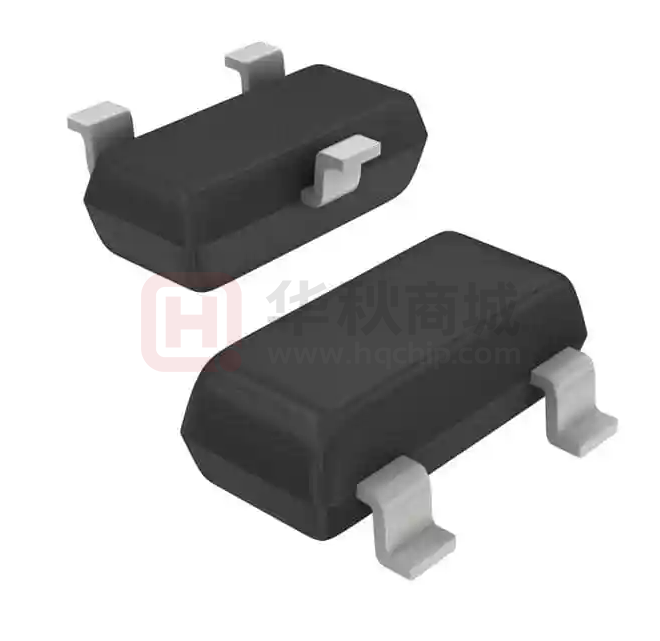
NP2N10MR
100V N-Channel Enhancement Mode MOSFET
Description
Schematic diagram
The NP2N10MR uses advanced trench technology
to provide excellent R DS(ON) , low gate charge and high
density cell Design for ultra low on-resistance. This
device is suitable for use as a load switch or in PWM
applications.
D
G
General Features
S
V DS =100V,I D =2A
R DS(ON) (Typ.)=220mΩ
@V GS =10V
R DS(ON) (Typ.)=240mΩ
@V GS =4.5V
High power and current handing capability
Lead free product is acquired
Surface mount package
Marking and pin assignment
SOT-23-3L
(TOP VIEW)
D
3
Application
NP102
PWM applications
Load switch
Package
SOT-23-3L
1
2
G
S
Ordering Information
Part Number
Storage Temperature
Package
Devices Per Reel
NP2N10MR-G
-55°C to +150°C
SOT-23-3L
3000
Absolute Maximum Ratings (TA=25℃ unless otherwise noted)
parameter
symbol
limit
unit
Drain-source voltage
V DS
100
V
Gate-source voltage
V GS
±20
V
Drain current-continuous@Tj=125℃
-pulse dC
ID
2
A
I DM
8
A
Drain-source Diode forward current
Is
2
A
Avalanche Current
I AS
4.8
A
E AS
6.3
mJ
Maximum power dissipation
PD
1.25
W
Operating junction Temperature range
Tj
-55—150
℃
Single Pulse Avalanche Energy
B
Rev.1.0 —Jan.8.2018
1
www.natlinear.com
�NP2N10MR
Electrical Characteristics (TA=25℃ unless otherwise noted)
Parameter
Symbol
Condition
Min
Typ
Max
Unit
OFF Characteristics
Drain-source breakdown voltage
BV DSS
V GS =0V, I D =250µA
100
-
-
V
Zero gate voltage drain current
I DSS
V DS =100V, V GS =0V
-
-
1
µA
Gate-body leakage
I GSS
V DS =0V, V GS =±20V
-
-
±100
nA
1.2
1.9
2.5
V
-
220
240
240
260
1
-
-
-
190
-
-
22
-
-
13
-
-
6
-
-
10
-
-
10
-
-
6
-
-
5.2
-
-
0.75
-
-
1.4
-
-
0.76
1.16
ON Characteristics
Gate threshold voltage
V GS(th)
Drain-source on-state resistance
R DS(ON)
Forward transconductance
V DS =V GS , I D =250µA
G FS
V GS =10V, I D =2A
V GS =4.5V, I D =2A
V DS =5V, I D =1A
mΩ
S
Dynamic Characteristics
Input capacitance
C ISS
Output capacitance
C OSS
Reverse transfer capacitance
C RSS
V DS =50V ,V GS =0V
f=1.0MHz
pF
Switching Characteristics
Turn-on delay time
t D(ON)
Rise time
V DD =50V
R L =39 ohm
V GS =10V
R G =1ohm
tr
Turn-off delay time
t D(OFF)
Fall time
tf
Total gate charge
Qg
Gate-source charge
Q gs
Gate-drain charge
Q gd
V DS =50V
I D =1.3A
V GS =10V
ns
nC
DRAIN-SOURCE DIODE CHARACTERISTICS
Diode forward voltage
V SD
V GS =0V,Is=2A
V
Thermal Characteristics
Parameter
Maximum Junction-to-Ambient
A
Maximum Junction-to-Ambient
AD
Maximum Junction-to-Lead
Symbol
t≤ 10s
Steady-State
Steady-State
R θJA
R θJL
Typ.
Max.
70
90
100
125
62
80
Unit
℃/W
2
A. The value of R θJA is measured with the device mounted on 1in FR-4 board with 2oz. Copper, in a still air environment with
T A =25°C. The value in any given application depends on the user's specific board design.
B. The power dissipation PD is based on T J(MAX) =150°C, using ≤ 10s junction-to-ambient thermal resistance.
C. Repetitive rating, pulse width limited by junction temperature T J(MAX) =150°C. Ratings are based on low frequency and duty
cycles to keep initialT J =25°C.
D. The R θJA is the sum of the thermal impedence from junction to lead R θJL and lead to ambient.
Rev.1.0 —Jan.8.2018
2
www.natlinear.com
�NP2N10MR
Typical Performance Characteristics
Rev.1.0 —Jan.8.2018
3
www.natlinear.com
�NP2N10MR
Rev.1.0 —Jan.8.2018
4
www.natlinear.com
�NP2N10MR
Rev.1.0 —Jan.8.2018
5
www.natlinear.com
�NP2N10MR
Package Information
SOT-23-3L
θ
D
b
E
E1
L
0.2
e
c
Symbol
Dimensions In Millimeters
A
A2
A1
e1
Dimensions In Inches
Min
Max
Min
Max
A
1.050
1.250
0.041
0.049
A1
0.000
0.100
0.000
0.004
A2
1.050
1.150
0.041
0.045
b
0.300
0.500
0.012
0.020
c
0.100
0.200
0.004
0.008
D
2.820
3.020
0.111
0.119
E
1.500
1.700
0.059
0.067
E1
2.650
2.950
0.104
0.116
e
0.950(BSC)
0.037(BSC)
e1
1.800
2.000
0.071
0.079
L
0.300
0.600
0.012
0.024
θ
0°
8°
0°
8°
Rev.1.0 —Jan.8.2018
6
www.natlinear.com
�
很抱歉,暂时无法提供与“NP2N10MR-G”相匹配的价格&库存,您可以联系我们找货
免费人工找货- 国内价格
- 10+0.36537
- 100+0.29031
- 300+0.25272
- 3000+0.21514
- 6000+0.19268
- 9000+0.18134
