XBLW 24C01
Two-Wire Serial EEPROM 1K(8-bit wide)
General Description
The 24C01 is 1024bits of serial Electrical Erasable and Programmable Read Only Memory, commonly
known as EEPROM. They are organized as 256 words of 8 bits (1 byte) each. The devices are fabricated with
proprietary advanced CMOS process for low power and low voltage applications. These devices are available in
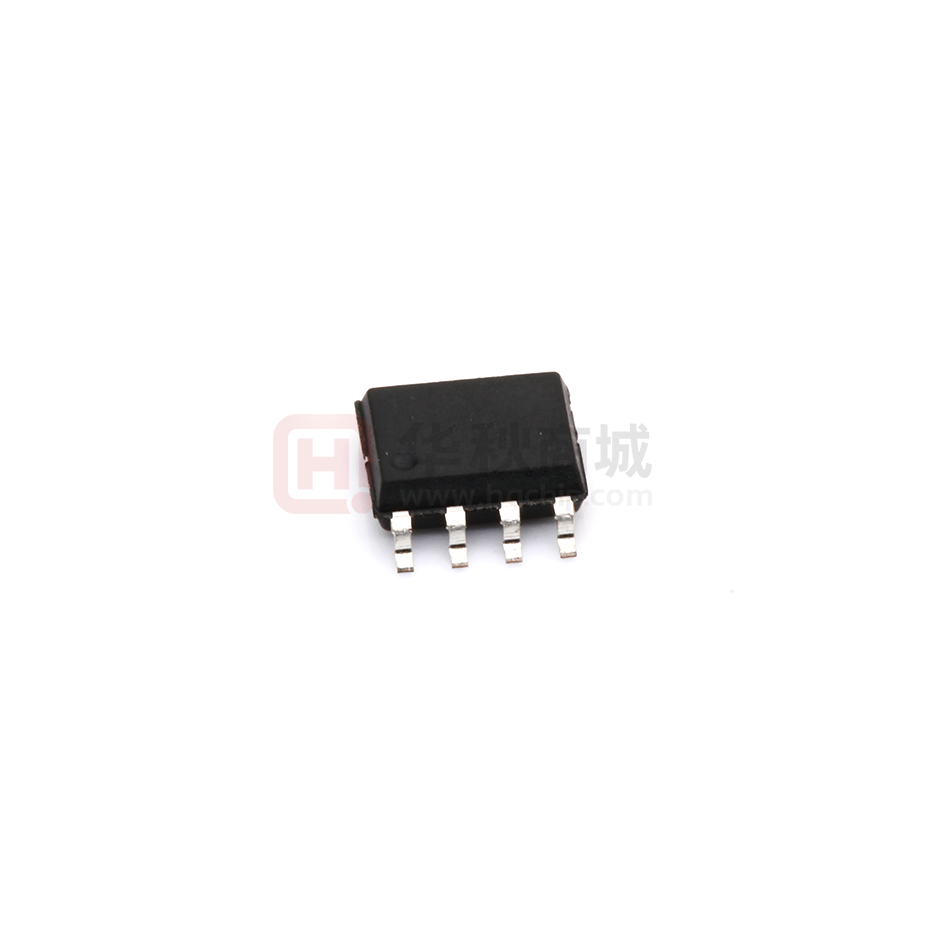
standard 8-lead DIP, 8-lead SOP, 8-lead MSOP, 8-lead TSSOP, 8-lead DFN and 5-lead SOT-23/TSOT-23
packages. A standard 2-wire serial interface is used to address all read and write functions. Our extended VCC
range (1.8V to 5.5V) devices enables wide spectrum of applications.
Features
Low voltage and low power operations:
· 24C01: VCC = 1.8V to 5.5V, Industrial temperature range (-40℃ to 85℃).
· 24C01: With 3 bits device address, the devices are suitable for all application. (For use of 5 pins package, the
device address A2,A1,and A0 bits must be set to zero)
16 bytes page write mode.
Partial page write operation allowed.
Internally organized: 256 × 4 (1K).
Standard 2-wire bi-directional serial interface.
Schmitt trigger, filtered inputs for noise protection.
Self-timed programming cycle (5ms maximum).
1 MHz (2.5-5V), 400 kHz (1.8V) Compatibility.
Automatic erase before write operation.
Write protect pin for hardware data protection.
High reliability: typically 1,000,000 cycles endurance.
100 years data retention.
Standard 8-pin DIP/SOP/MSOP/TSSOP/DFN and 5-pin SOT-23/TSOT-23 Pb-free packages.
Order Information
Product Model
Package Type
Marking
Packing
Packing Qty
24C01S
SOT23-5
24C01S
Tape
3000/Reel
24C01N
DIP-8
24C01N
Tube
2000/Box
24C01BN
SOP-8
24C01BN
Tape
4000/Reel
XBLWversion1.0
文档仅供参考,实际应用测试为准
www.xinboleic.com
技术支持热线:4009682003
第 1 页 共 15 页
�XBLW 24C01
Two-Wire Serial EEPROM 1K(8-bit wide)
PIN CONFIGURATION
Pin Name
A2, A1, A0
SDA
Pin Function
Device Address Inputs
Serial Data Input / Open Drain Output
SCL
Serial Clock Input
WP
Write Protect
VCC
Power Supply
GND
Ground
NC
No- Connect
Table 1
All these packaging types come in conventional or Pb- free certified.
Figure 1: Package types
ABSOLUTE MAXIMUM RATINGS
Industrial operating temperature .......................................................................................................................... -4 0 C to 8 5 C
Storage temperature ............................................................................................................................................. -5 0 C to 12 5 C
Input voltage on any pin relative to ground ............................................................................................. -0.3V to VCC + 0.3V
Maximum voltage ........................................................................................................................................................................ 8V
ESD protection on all pins ................................................................................................................................................ >2000V
* Stresses exceed those listed under “ Absolute Maximum Rating” may cause permanent damage to the
device. Functional operation of the device at conditions beyond those listed in the specification is not
guaranteed. Prolonged exposure to extreme conditions may affect device reliability or functionality.
XBLWversion1.0
文档仅供参考,实际应用测试为准
www.xinboleic.com
技术支持热线:4009682003
第 2 页 共 15 页
�XBLW 24C01
Two-Wire Serial EEPROM 1K(8-bit wide)
Block Diagram And Pin Description
Block Diagram
Figure 2: Block Diagram
PIN DESCRIPTIONS
(A) SERIAL CLOCK (SCL)
The rising edge of this SCL input is to latch data into the EEPROM device while the falling edge of this clock is to
clock data out of the EEPROM device.
(B) SERIAL DATA LINE (SDA)
SDA data line is a bi- directional signal for the serial devices. It is an open drain output signal and can be wiredOR with other open- drain output devices.
( C) DEVICE / CHIP SELECT ADDRESSES (A2, A1, A0)
These are the chip select input signals for the serial EEPROM devices. Typically, these signals are hardwired to
either VIH or VIL. If left unconnected, they are internally recognized as VIL. However, due to capacitive coupling
that may appear in customer applications,
recommends always connecting the address pins to a knownstate .
When using a pull-up or pull-down resistor, recommends using 10 kΩ or less.
(D) WRITE PROTECT (WP)
The 2 4 C0 1 devices have a WP pin to protect the whole EEPROM array from programming. Programming
operations are allowed if WP pin is left un- connected or input to VIL. Conversely all programming functions are
disabled if WP pin is connected to VIH or VCC. Read operations is not affected by the WP pin’s input level.
If left
unconnected, it is internally recognized as VIL. However, due to capacitive coupling that may appear in
customer applications, recommends always connecting the WP pin to a known state. When using a pull-up
or pulldown resistor, recommends using 10kΩ or less.
XBLWversion1.0
文档仅供参考,实际应用测试为准
www.xinboleic.com
技术支持热线:4009682003
第 3 页 共 15 页
�XBLW 24C01
Two-Wire Serial EEPROM 1K(8-bit wide)
MEMORY ORGANIZATION
The 24 C01 devices have 16 pages. Since each page has 16 bytes, random word addressing to 24 C01
will require 8 bits data word addresses.
DEVICE OPERATION
( A) SERIAL CLOCK AND DATA TRANSITIONS
The SDA pin is typically pulled to high by an external resistor.
Data is allowed to change only when Serial clock
SCL is at VIL . Any SDA signal transition may interpret as either a START or STOP condition as described below.
( B) START CONDITION
With SCL ≥ VIH , a SDA transition from high to low is interpreted as a START condition.
All valid commands
must begin with a START condition.
( C) STOP CONDITION
With SCL ≥ VIH, a SDA transition from low to high is interpreted as a STOP condition.
All valid read or write
commands end with a STOP condition. The device goes into the STANDBY mode if it is after a read command.
A STOP condition after page or byte write command will trigger the chip into the STANDBY mode after the selftimed internal programming finish.
( D) ACKNOWLEDGE
The 2-wire protocol transmits address and data to and from the EEPROM in 8 bit words. The EEPROM
acknowledges the data or address by outputting a " 0 " after receiving each word. The ACKNOWLEDGE signal
occurs on the 9 th serial clock after each word.
(E) STANDBY MODE
The EEPROM goes into low power STANDBY mode after a fresh power up, after receiving a STOP bit in read
mode, or after completing a self- time internal programming operation.
(F) SOFT RESET
After an interruption in protocol power loss or system reset, any two- wire part can be reset by following these
steps:
1. Creat a START condition,
2. Clock eighteen data bits “1” ,
3. Creat a start condition as SDA is high.
Figure 3 : Timing diagram for START and STOP conditions
XBLWversion1.0
文档仅供参考,实际应用测试为准
www.xinboleic.com
技术支持热线:4009682003
第 4 页 共 15 页
�XBLW 24C01
Two-Wire Serial EEPROM 1K(8-bit wide)
Figure 4 : Timing diagram for output ACKNOWLEDGE
DEVICE ADDRESSING
The 2 - wire serial bus protocol mandates an 8 bits device address word after a START bit condition to invoke
valid read or write command.
The first four most significant bits of the device address must be 1 0 1 0 , which is
common to all serial EEPROM devices. The next three bits are device address bits. These three device address
bits ( 5 th , 6 th and 7 th) are to match with the external chip select/ address pin states.
EEPROM device outputs an ACKNOWLEDGE signal after the 8
th
If a match is made, the
read/ write bit, otherwise the chip will go into
STANDBY mode.
The last or 8 th bit is a read/ write command bit. If the 8 th bit is at VIH then the chip goes into read mode. If a “0 ”
is detected, the device enters programming mode.
WRITE OPERATIONS
(A) BYTE WRITE
A byte write operation starts when a micro- controller sends a START bit condition, follows by a proper EEPROM
device address and then a write command.
EEPROM device will acknowledge at the
8 bits word address.
9 th
If the device address bits match the chip select address, the
clock cycle. The micro- controller will then send the rest of the lower
At the 1 8 th cycle, the EEPROM will acknowledge the 8 - bit address word.
The micro-
controller will then transmit the 8 bit data. Following an ACKNOWLDEGE signal from the EEPROM at the 2 7 th
clock cycle, the micro- controller will issue a STOP bit.
After receiving the STOP bit, the EEPROM will go into a
self- timed programming mode during which all external inputs will be disabled.
After a programming time of TWC,
the byte programming will finish and the EEPROM device will return to the STANDBY mode.
(B) PAGE WRITE
A page write is similar to a byte write with the exception that one to sixteen bytes can be programmed along the
same page or memory row. All 24 C01 are organized to have 16 bytes per memory row or page.
With the same write command as the byte write, the micro- controller does not issue a STOP bit after sending the
1 st byte data and receiving the ACKNOWLEDGE signal from the EEPROM on the 2 7 th clock cycle.
sends out a second 8 - bit data word, with the EEPROM acknowledging at the
3 6 th
Instead it
cycle. This data sending and
EEPROM acknowledging cycle repeats until the micro- controller sends a STOP bit after the n × 9 th clock cycle.
After which the EEPROM device will go into a self- timed partial or full page programming mode.
After the page
programming completes after a time of TWC, the devices will return to the STANDBY mode.
XBLWversion1.0
文档仅供参考,实际应用测试为准
www.xinboleic.com
技术支持热线:4009682003
第 5 页 共 15 页
�XBLW 24C01
Two-Wire Serial EEPROM 1K(8-bit wide)
The least significant 4 bits of the word address ( column address) increments internally by one after receiving
each data word.
The rest of the word address bits ( row address) do not change internally, but pointing to a
specific memory row or page to be programmed.
The first page write data word can be of any column address.
Up to 16 data words can be loaded into a page. If more then 16 data words are loaded, the 1 7 th data word will
be loaded to the 1 st data word column address. The 1 8 th data word will be loaded to the 2 nd data word column
address and so on. In other word, data word address (column address) will “roll” over the previously loaded data.
( C) ACKNOWLEDGE POLLING
ACKNOWLEDGE polling may be used to poll the programming status during a self-timed internal programming. By
issuing a valid read or write address command, the EEPROM will not acknowledge at the 9th clock cycle if the device is
still in the self-timed programming mode. However, if the programming completes and the chip has returned to the
STANDBY mode, the device will return a valid ACKNOWLEDGE signal at the 9th clock cycle.
READ OPERATIONS
The read command is similar to the write command except the 8th read/write bit in address word is set to “1” . The
three read operation modes are described as follows:
(A) CURRENT ADDRESS READ
The EEPROM internal address word counter maintains the last read or write address plus one if the power supply
to the device has not been cut off. To initiate a current address read operation, the micro-controller issues a START
bit and a valid device address word with the read/write bit (8th) set to “1” . The EEPROM will response with an
ACKNOWLEDGE signal on the 9th serial clock cycle. An 8-bit data word will then be serially clocked out. The
internal address word counter will then automatically increase by one. For current address read the micro-controller
will not issue an ACKNOWLEDGE signal on the 18th clock cycle. The micro-controller issues a valid STOP bit after
the 18th clock cycle to terminate the read operation. The device then returns to STANDBY mode.
(B) SEQUENTIAL READ
The sequential read is very similar to current address read. The micro-controller issues a START bit and a valid device
address word with read/write bit (8th) set to “1” . The EEPROM will response with an ACKNOWLEDGE signal on the
9th serial clock cycle. An 8-bit data word will then be serially clocked out. Meanwhile the internally address word
counter will then automatically increase by one. Unlike current address read, the micro-controller sends an
ACKNOWLEDGE signal on the 18th clock cycle signaling the EEPROM device that it wants another byte of data.
Upon receiving the ACKNOWLEDGE signal, the EEPROM will serially clocked out an 8-bit data word based on the
incremented internal address counter. If the micro-controller needs another data, it sends out an ACKNOWLEDGE
signal on the 27th clock cycle. Another 8-bit data word will then be serially clocked out. This sequential read cont
(C) RANDOM READ
Random read is a two-steps process. The first step is to initialize the internal address counter with a target read
address using a “dummy write” instruction. The second step is a current address read.
To initialize the internal address counter with a target read address, the micro-controller issues a START bit first,
follows by a valid device address with the read/write bit (8th) set to “0” . The EEPROM will then acknowledge. The
micro-controller will then send the address word. Again the EEPROM will acknowledge. Instead of sending a valid
written data to the EEPROM, the micro-controller performs a current address read instruction to read the data. Note
that once a START bit is issued, the EEPROM will reset the internal programming process and continue to execute
the new instruction - which is to read the current address.
XBLWversion1.0
文档仅供参考,实际应用测试为准
www.xinboleic.com
技术支持热线:4009682003
第 6 页 共 15 页
�XBLW 24C01
Two-Wire Serial EEPROM 1K(8-bit wide)
XBLWversion1.0
文档仅供参考,实际应用测试为准
www.xinboleic.com
技术支持热线:4009682003
第 7 页 共 15 页
�XBLW 24C01
Two-Wire Serial EEPROM 1K(8-bit wide)
Electrical Specifications
( A)
Power- Up Requirements
During a power- up sequence, the VCC supplied to the device should monotonically rise from GND to the
minimum VCC level, with a slew rate no faster than 0.05 V/μs and no slower then 0. 1 V/ms. A decoupling cap
should be connected to the VCC PAD which is no smaller than 10 nF.
( B) Device Reset
To prevent inadvertent write operations or any other spurious events from occurring during a power- up
sequence, this device includes a Power- on Reset ( POR) circuit. Upon power- up, the device will not respond to
any commands until the VCC level crosses the internal voltage threshold ( VPOR) that brings the device out of
Reset and into Standby mode. The system designer must ensure the instructions are not sent to the device until
the VCC supply has reached a stable value greater than or equal to the minimum VCC level.
XBLWversion1.0
文档仅供参考,实际应用测试为准
www.xinboleic.com
技术支持热线:4009682003
第 8 页 共 15 页
�XBLW 24C01
Two-Wire Serial EEPROM 1K(8-bit wide)
Figure 1 1: Power on and Power down
If an event occurs in the system where the VCC level supplied to the device drops below the maximum VPOR
level specified, it is recommended that a full power cycle sequence be performed by first driving the VCC pin to
GND, waiting at least the minimum tPOFF time and then performing a new power- up sequence in compliance with
the requirements defined in this section.
AC CHARACTERISTICS
Symbol
f SCL
tLOW
tHIGH
tI
tAA
Parameter
1.8 V
Min
Clock frequency, SCL
tHD. STA
tSU. STA
tHD. DAT
tSU. DAT
tR
tF
tSU. STO
tDH
tPWR,R( 1)
tPUP( 1)
tPOFF( 1)
Max
Min
Unit
Max
Clock pulse width low
1.3
0.4
kHz
µs
Clock pulse width high
0.6
0.4
µs
Noise suppression
tBUF
2.5V-5.5 V
time( 1)
400
1000
50
50
ns
0.55
µs
Clock low to data out valid
Time the bus must be free
before a new transmission can
start( 1)
0.2
1.3
0.5
µs
START hold time
0.6
0.25
µs
START set- up time
0.6
0.25
µs
0
0
µs
100
100
ns
Data in hold time
Data in set-up time
Input rise
Input fall
time( 1)
time( 1)
0.9
0.2
0.3
0.3
µs
300
100
ns
STOP set- up time
0.6
0.25
µs
Date out hold time
50
50
ns
Vcc slew rate at power up
0.1
Time required after VCC is
stable before the device can
accept commands
100
100
µs
Minimum time at Vcc= 0 V
between power cycles
500
500
ms
tWR
Write cycle time
Endurance( 1)
25 oC,
50
0.1
5
Page Mode, 3.3V
V/ ms
50
ms
5
1,000,000
Write Cycles
Notes: 1. This Parameter is expected by characterization but is not fully screened by test.
2 . AC Measurement conditions:
RL (Connects to Vcc): 1.3KΩ
Input Pulse Voltages: 0.3Vcc to 0.7Vcc
Input and output timing reference Voltages: 0. 5 Vcc
XBLWversion1.0
文档仅供参考,实际应用测试为准
www.xinboleic.com
技术支持热线:4009682003
第 9 页 共 15 页
�XBLW 24C01
Two-Wire Serial EEPROM 1K(8-bit wide)
DC CHARACTERISTICS
Symbol
Parameter
Test Conditions
Min
Typical
Max
Unit
s
5.5
V
VCC1
Power supply VCC
ICC1
Supply read current
VCC @ 5.0V SCL = 400 kHz
0.5
1.0
mA
ICC2
Supply write current
VCC @ 5.0V SCL = 400 kHz
2.0
3.0
mA
ISB1
Supply current
VCC @ 1.8V, VIN = VCC or VSS
< 1.0
µA
ISB2
Supply current
VCC @ 2.5V, VIN = VCC or VSS
< 1.0
µA
ISB3
Supply current
VCC @ 5.0V, VIN = VCC or VSS
< 1.0
µA
IIL
Input leakage current
VIN = VCC or VSS
3.0
µA
VIN = VCC or VSS
3.0
µA
1.8
VIL
Output leakage
current
Input low level
VIH
Input high level
VOL1
Output low level
VCC @ 1.8V, IOL = 0. 15 mA
0.2
V
VOL2
Output low level
VCC @ 3.0V, IOL = 2. 1 mA
0.4
V
ILO
XBLWversion1.0
-0.6
VCC × 0.3
V
VCC × 0.7
VCC + 0.5
V
文档仅供参考,实际应用测试为准
www.xinboleic.com
技术支持热线:4009682003
第 10 页 共 15 页
�XBLW 24C01
Two-Wire Serial EEPROM 1K(8-bit wide)
Package Information
DIP8
XBLWversion1.0
文档仅供参考,实际应用测试为准
www.xinboleic.com
技术支持热线:4009682003
第 11 页 共 15 页
�XBLW 24C01
Two-Wire Serial EEPROM 1K(8-bit wide)
TSSOP8
XBLWversion1.0
文档仅供参考,实际应用测试为准
www.xinboleic.com
技术支持热线:4009682003
第 12 页 共 15 页
�XBLW 24C01
Two-Wire Serial EEPROM 1K(8-bit wide)
SOP8
XBLWversion1.0
文档仅供参考,实际应用测试为准
www.xinboleic.com
技术支持热线:4009682003
第 13 页 共 15 页
�XBLW 24C01
Two-Wire Serial EEPROM 1K(8-bit wide)
MSOP8
XBLWversion1.0
文档仅供参考,实际应用测试为准
www.xinboleic.com
技术支持热线:4009682003
第 14 页 共 15 页
�XBLW 24C01
Two-Wire Serial EEPROM 1K(8-bit wide)
Statement:
Shenzhen xinbole electronics co., ltd. reserves the right to change the product specifications, without notice!
Before placing an order, the customer needs to confirm whether the information obtained is the latest version,
and verify the integrity of the relevant information.
Any semiconductor product is liable to fail or malfunction under certain conditions, and the buyer shall be
responsible for complying with safety standards in the system design and whole machine manufacturing using
Shenzhen xinbole electronics co., ltd products, and take appropriate security measures to avoid the potential risk
of failure may result in personal injury or property losses of the situation occurred!
Product performance is never ending, Shenzhen xinbole electronics co., ltd will be dedicated to provide
customers with better performance, better quality of integrated circuit products.
XBLWversion1.0
文档仅供参考,实际应用测试为准
www.xinboleic.com
技术支持热线:4009682003
第 15 页 共 15 页
�