L7805
Wide VIN 1.5A Fixed Voltage Regulators
General Description
The L7805 Family monolithic 3-terminal positive voltage regulators empIOy internal
currentlimiting, thermal shutdown and safe-area compensation, making them essentially
indestructible. If adequate heat sinking is provided, they can deliver over 1.5-A output
current. They are intended as fixed voltage regulators in a wide range of applications
including IOcal (on-card) regulation for elimination of noise and distribution problems
associated with single-point regulation. In addition to use as fixed voltage regulators,
these devices can be used with external components to obtain adjustable output voltages
and currents.
Considerable effort was expended to make the entire series of regulators easy to
use and minimize the number of external components. It is not necessary to bypass the
output, although this does improve transient response. Input bypassing is needed only if the regulator is
IOcated far from the filter capacitor of the power supply.
Features
Output Current up to 1.5 A
Available in Fixed 5-V, 12-V, and 15-V Options
Internal Thermal OverIOad, Short-Circuit and SOA Protection
Available in Space-SaVINg SOT-223 Package
Output Capacitance Not Required for Stability
Ordering Information
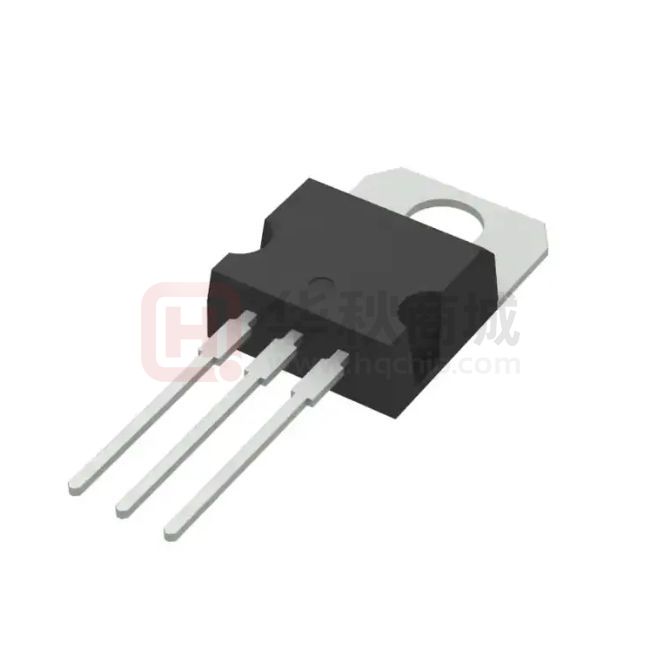
DEVICE
L7805CV
Package Type
TO-220
MARKING
Packing
L7805CV
Tube
Packing QTY
1000/BOX
Applications
Industrial Power Supplies
SMPS Post Regulation
HVAC Systems
AC Inventors
Test and Measurement Equipment
Brushed and Brushless DC Motor Drivers
Solar Energy String Invertors
XBLWversion1.0
www.xinboleic.com
技术支持热线:4009682003
文档仅供参考,实际应用测试为准
第 1 页 共 12 页
�L7805
Wide VIN 1.5A Fixed Voltage Regulators
Pin Functions
PIN
NAME
INPUT
GND
OUTPUT
NO.
1
2
3
I/O
I
I/O
O
DESCRIPTION
Input voltage pin
Ground pin
Output voltage pin
Absolute Maximum Ratings
MIN
MAX
UNIT
35
V
DC input voltage
Internal power dissipation
Internally Limited
(3)
Maximum junction temperature
Lead temperature (soldering,
10 sec.)
TO-3 package (NDS)
Lead temperature 1,6 mm (1/16 in) from case for 10 s
Storage temperature
-65
150
℃
300
℃
230
℃
150
℃
(1)Stresses beyond those listed under Absolute Maximum Ratings may cause permanent damage to the device.
These are stress ratings only, which do not imply functional operation of the device at these or any other
conditions beyond those indicated under Recommended Operating Conditions. Exposure to absolute-maximumrated conditions for extended periods may affect device reliability.
(2)If Military/Aerospace specified devices are required, please contact the Texas Instruments Sales
Office/Distributors for availability and specifications.
(3)The maximum alIOwable power dissipation at any ambient temperature is a function of the maximum junction
temperature for operation (TJMAX = 125℃ or 150℃), the junction-to-ambient thermal resistance (θJA), and the
ambient temperature (TA). PDMAX = (TJMAX − TA)/θJA. If this dissipation is exceeded, the die temperature rises
above TJMAX and the electrical specifications do not apply. If the die temperature rises above 150℃, the device
goes into thermal shutdown. For the TO-3 package (NDS), the junction-to-ambient thermal resistance (θJA) is 39
℃/W. When using a heat sink, θJA is the sum of the 4℃/W junction-to-case thermal resistance (θJC) of the TO-3
package and the case-to-ambient thermal resistance of the heat sink. For the TO-220 package (NDE), θJA is 54
℃/W and θJC is 4℃/W.
ESD Ratings
V(ESD)
Electrostatic
dischareg
Human-body model(HBM)(1)
MAX
UNIT
±2000
V
(1)ESD rating is based on the human-body model, 100pF discharged through 1.5kΩ.
Thermal Information
THERMAL METRIC(1)
RθJA
RθJC(top)
Junction-to-ambient thermal resistance
Junction-to-case (top) thermal resistance
L7805 Family
NDE
(TO-220)
23.9
UNIT
℃/W
16.7
℃/W
RθJB
Junction-to-board thermal resistance
5.3
℃/W
ψJT
Junction-to-top characterization parameter
3.2
℃/W
XBLWversion1.0
www.xinboleic.com
技术支持热线:4009682003
文档仅供参考,实际应用测试为准
第 2 页 共 12 页
�L7805
Wide VIN 1.5A Fixed Voltage Regulators
ψJB
RθJC(bot)
Junction-to-board characterization parameter
5.3
℃/W
Junction-to-case (bottom) thermal resistance
1.7
℃/W
(1)For more information about traditional and new thermal metrics, see the Semiconductor and IC Package Thermal Metrics application report.
Electrical Characteristics (VO=5V,VI=10V,0℃≤TJ≤125℃ unless otherwise specified(1))
PARAMETER
VO Output voltage
∆VO Line regulation
∆VO IOad regulation
IQ Quiescent current
∆IQ Quiescent current change
VN Output noise voltage
∆���
∆����
RO
VIN
Ripple rejection
Dropout voltage
Output resistance
Short-circuit current
Peak output current
Average TC of Vout
Input voltage required to
maintain line regulation
TEST CONDITIONS
TJ=25℃,5 mA≤IO≤1A
PD≤15W,5 mA≤IO≤1A
7.5V≤VIN≤20V
TJ=25℃
7V≤VIN≤25V
IO=500mA
Over temperature
8V≤VIN≤20V
TJ=25℃
7.5V≤VIN≤20V
IO≤1A
Over temperature
8V≤VIN≤12V
5mA≤IO≤1.5A
TJ=25℃
250mA≤IO≤750mA
Over temperature,5mA≤IO≤1A
TJ =25℃
IO≤1A
Over temperature
0℃≤TJ≤125℃,5mA≤IO≤1A
TJ=25℃,IO≤1A
7V≤VIN≤20V
Over temperature, IO≤ 500mA
TA=25℃,10Hz≤f≤100kHz
TJ=25℃,IO≤1A
f=120Hz
8V≤VIN≤18V
Over temperature, IO≤500mA
TJ=25℃,IO=1A
f=1kHz
TJ=25℃
TJ=25℃
Over temperature, IO = 5 mA
TJ=25℃,IO≤1A
MIN
4.8
TYP
5
MAX
5.2
UNIT
V
5.25
V
50
mV
50
mV
50
mV
25
mV
50
25
50
8
8.5
mV
mV
mV
mA
mA
mA
mA
mA
μV
dB
dB
V
mQ
A
A
mV/℃
4.75
3
10
0.5
1
1
62
62
40
80
2
8
2.1
2.4
-0.6
7.5
V
(1)All characteristics are measured with a 0.22-μF capacitor from input to ground and a 0.1-μF capacitor from output to ground. All characteristics
except noise voltage and ripple rejection ratio are measured using pulse techniques (tw ≤ 10 ms, duty cycle ≤ 5%). Output voltage changes due to
changes in internal temperature must be taken into account separately.
XBLWversion1.0
www.xinboleic.com
技术支持热线:4009682003
文档仅供参考,实际应用测试为准
第 3 页 共 12 页
�L7805
Wide VIN 1.5A Fixed Voltage Regulators
Typical Characteristics
XBLWversion1.0
www.xinboleic.com
技术支持热线:4009682003
文档仅供参考,实际应用测试为准
第 4 页 共 12 页
�L7805
Wide VIN 1.5A Fixed Voltage Regulators
Typical Characteristics (continued)
XBLWversion1.0
www.xinboleic.com
技术支持热线:4009682003
文档仅供参考,实际应用测试为准
第 5 页 共 12 页
�L7805
Wide VIN 1.5A Fixed Voltage Regulators
Typical Characteristics (continued)
Application Information
The L7805 series is designed with thermal protection, output short-circuit protection, and output
transistor safe area protection. However, as with any IC regulator, it becomes necessary to take
precautions to assure that the regulator is not inadvertently damaged. The following describes possible
misapplications and methods to prevent damage to the regulator.
Shorting the Regulator Input
XBLWversion1.0
www.xinboleic.com
技术支持热线:4009682003
文档仅供参考,实际应用测试为准
第 6 页 共 12 页
�L7805
Wide VIN 1.5A Fixed Voltage Regulators
When using large capacitors at the output of these regulators, a protection diode connected input
to output (Figure 15) may be required if the input is shorted to ground. Without the protection diode,
an input short causes the input to rapidly approach ground potential, while the output remains near
the initial VOUT because of the stored charge in the large output capacitor. The capacitor will then
discharge through a large internal input to output diode and parasitic transistors. If the energy
released by the capacitor is large enough, this diode, low current metal, and the regulator are
destroyed. The fast diode in Figure 15 shunts most of the capacitors discharge current around the
regulator. Generally no protection diode is required for values of output capacitance
≤ 10μF.
Raising the Output Voltage Above the Input Voltage
Because the output of the device does not sink current, forcing the output high can cause damage to internal low
current paths in a manner similar to that just described in Shorting the Regulator Input.
Regulator Floating Ground
When the ground pin alone becomes disconnected, the output approaches the unregulated input,
causingpossible damage to other circuits connected to VOUT. If ground is reconnected with power ON,
damage may also occur to the regulator. This fault is most likely to occur when plugging in regulators or
modules with on card regulators into powered up sockets. The power must be turned off first, the thermal
limit ceases operating, or the ground must be connected first if power must be left on. See Figure 16.
Transient Voltages
If transients exceed the maximum rated input voltage of the device, or reach more than 0.8V below
ground and have sufficient energy, they will damage the regulator. The solution is to use a large input
capacitor, a series input breakdown diode, a choke, a transient suppressor or a combination of these.
Figure 15. Input Short
Figure 16. Regulator Floating Ground
XBLWversion1.0
www.xinboleic.com
技术支持热线:4009682003
文档仅供参考,实际应用测试为准
第 7 页 共 12 页
�L7805
Wide VIN 1.5A Fixed Voltage Regulators
Figure 17. Transients
When a value for θ(H–A) is found, a heat sink must be selected that has a value that is less than or
equal to this number.
θ(H–A) is specified numerically by the heat sink manufacturer in this catalog or shown in a curve that
plots temperature rise vs power dissipation for the heat sink.
Fixed Output Voltage Regulator
The L7805 Family devices are primarily designed to provide fixed output voltage regulation. The
simplest implementation of L7805 Family is shown in Figure18.
Figure 18. Fixed Output Voltage Regulator
Design Requirements
The device component count is very minimal. Although not required, TI recommends employing
bypass capacitors at the output for optimum stability and transient response. These capacitors
must be placed as close as possible to the regulator. If the device is located more than 6 inches
from the power supply filter, it is required to employ input capacitor.
Detailed Design Procedure
The output voltage is set based on the device variant. LM340x and L7805 Family are available
in 5-V, 12-V and 15-V regulator options.
XBLWversion1.0
www.xinboleic.com
技术支持热线:4009682003
文档仅供参考,实际应用测试为准
第 8 页 共 12 页
�L7805
Wide VIN 1.5A Fixed Voltage Regulators
Application Curve
Figure 19. VOUT vs VIN, VOUT = 5V
XBLWversion1.0
www.xinboleic.com
技术支持热线:4009682003
文档仅供参考,实际应用测试为准
第 9 页 共 12 页
�L7805
Wide VIN 1.5A Fixed Voltage Regulators
System Examples
Figure 20. Current Regulator Figure
21. Adjustable Output Regulator
Figure 22. High Input Voltage Circuit With Series
Figure 23. High Input Voltage Circuit
implementation With Transistor
Figure 24. High Current Voltage Regulatorure
Figure25. High Output Current With ShortCircuit Protection
XBLWversion1.0
www.xinboleic.com
技术支持热线:4009682003
文档仅供参考,实际应用测试为准
第 10 页 共 12 页
�L7805
Wide VIN 1.5-A Fixed Voltage Regulators
Outline Drawing
TO220
XBLWversion1.0
Unit:mm
文档仅供参考,实际应用测试为准
www.xinboleic.com
技术支持热线:4009682003
第 11 页 共 12 页
�L7805
Wide VIN 1.5-A Fixed Voltage Regulators
Statement:
Shenzhen xinbole electronics co., ltd. reserves the right to change the product specifications, without notice!
Before placing an order, the customer needs to confirm whether the information obtained is the latest version,
and verify the integrity of the relevant information.
Any semiconductor product is liable to fail or malfunction under certain conditions, and the buyer shall be
responsible for complying with safety standards in the system design and whole machine manufacturing using
Shenzhen xinbole electronics co., ltd products, and take appropriate security measures to avoid the potential risk
of failure may result in personal injury or property losses of the situation occurred!
Product performance is never ending, Shenzhen xinbole electronics co., ltd will be dedicated to provide
customers with better performance, better quality of integrated circuit products.
XBLWversion1.0
文档仅供参考,实际应用测试为准
www.xinboleic.com
技术支持热线:4009682003
第 12 页 共 12 页
�