XBLW 74HC/HCT161
SYNCHRONOUS 4-BIT COUNTERS
General Description
The SN74HC/HCT161 is a synchronous presettable binary counter with an internal look-head carry.
Synchronous operation is provided by having all flip-flops clocked simultaneously on the positive-going edge of the
clock (CP). The outputs (Q0 to Q3) of the counters may be preset HIGH or LOW. A LOW at the parallel enable input
(P�) disables the counting action and causes the data at the data inputs (D0 to D3) to be loaded into the counter on the
positive-going edge of the clock. Preset takes place regardless of the levels at count enable inputs (CEP and CET). A
LOW at the master reset input (M�) sets Q0 to Q3 LOW regardless of the levels at input pins CP, P�, CET and CEP
(thus providing an asynchronous clear function). The look-ahead carry simplifies serial cascading of the counters.
Both CEP and CET must be HIGH to count. The CET input is fed forward to enable the terminal count output (TC).
The TC output thus enabled will produce a HIGH output pulse of a duration approximately equal to a HIGH output of
Q0. This pulse can be used to enable the next cascaded stage. The maximum clock frequency for the cascaded
counters is determined by the CP to TC propagation delay and CEP to CP set-up time, according to the following
formula: fmax=1/(tP(max)(CP to TC)+tSU(CEP to CP))
Inputs include clamp diodes. This enables the use of current limiting resistors to interface inputs to voltages in
excess of VCC.
Features
Input levels:
For SN74HC161: CMOS level
For SN74HCT161: TTL level
Synchronous counting and loading
2 count enable inputs for n-bit cascading
Asynchronous reset
Positive-edge triggered clock
Specified from -40℃ to +105℃
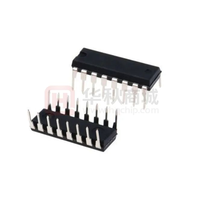
Packaging information: DIP16/SOP16/TSSOP16
ORDERING INFORMATION
DEVICE
Package Type
MARKING
Packing
Packing QTY
SN74HC161N
SN74HC161DTR
SN74HCT161DTR
SN74HCT161TDTR
DIP-16
SOP-16
SOP-16
TSSOP-16
74HC161N
74HC161
74HCT161
74HCT161
Tube
Tape
Tape
Tape
1000/Box
2500/Reel
2500/Reel
3000/Reel
XBLW version 1.0
文档仅供参考,实际应用测试为准
www.xinboleic.com 技术支持热线:4009682003
第 1 页 共 21 页
�XBLW 74HC/HCT161
SYNCHRONOUS 4-BIT COUNTERS
Block Diagram And Pin Description
Block Diagram
Figure 1. Logic symbol
Figure 2. IEC Logic symbol
Figure 3. Functional diagram
XBLW version 1.0
文档仅供参考,实际应用测试为准
www.xinboleic.com 技术支持热线:4009682003
第 2 页 共 21 页
�XBLW 74HC/HCT161
SYNCHRONOUS 4-BIT COUNTERS
Figure 4. Logic diagram
Figure 5. State diagram
XBLW version 1.0
Figure 6. Typical timing sequence
文档仅供参考,实际应用测试为准
www.xinboleic.com 技术支持热线:4009682003
第 3 页 共 21 页
�XBLW 74HC/HCT161
SYNCHRONOUS 4-BIT COUNTERS
Pin Configurations
Pin Description
Pin No.
Pin Name
Description
1
2
3
4
5
6
7
8
9
10
11
12
13
14
15
16
M�
CP
D0
D1
D2
D3
CEP
GND
P�
CET
Q3
Q2
Q1
Q0
TC
VCC
asy nchronous master reset(active LOW)
clock input(LOW-to-HIGH,edge triggered)
data input
data input
data input
data input
count enable input
ground(0V)
parallel enable input(active LOW)
count enable carry input
flip-flop output
flip-flop output
flip-flop output
flip-flop output
terminal count output
supply voltage
XBLW version 1.0
文档仅供参考,实际应用测试为准
www.xinboleic.com 技术支持热线:4009682003
第 4 页 共 21 页
�XBLW 74HC/HCT161
SYNCHRONOUS 4-BIT COUNTERS
Function Table
Input
Operating mode
M�
L
H
H
H
H
H
reset(clear)
parallel load
count
hold(do nothing)
CP
X
↑
↑
↑
X
X
CEP
X
X
X
h
l
X
CET
X
X
X
h
X
l
Output
P�
X
l
l
h
h
h
Dn
X
l
h
X
X
X
Qn
L
L
H
count
qn
qn
TC
L
L
[2]
[2]
[2]
L
Note:
[1] H=HIGH voltage level; L=LOW voltage level; X=don’t care; ↑=LOW-to-HIGH clock transition;
l=LOW voltage level one set-up time prior to the LOW-to-HIGH clock transition;
h=HIGH voltage level one set-up time prior to the LOW-to-HIGH CP transition;
q=lower case letters indicate the state of the referenced output one set-up time prior to the LOW-to-HIGH CP
transition.
[2] The TC output is HIGH when CET is HIGH and the counter is at terminal count (HLLH).
Electrical Parameter
Absolute Maximum Ratings (Voltages are referenced to GND (ground=0V), unless otherwise specified.)
Parameter
Symbol
Conditions
Min.
Max.
Unit
supply voltage
input clamping current
output clamping current
output current
supply current
ground current
storage temperature
total power dissipation
VCC
IIK
IOK
IO
ICC
IGND
Tstg
Ptot
-0.5
-50
-65
-
+7.0
±20
±20
±25
+50
+150
500
V
mA
mA
mA
mA
mA
℃
mW
soldering temperature
TL
VI < -0.5V or VI > VCC +0.5V
VO < -0.5V or VO > VCC +0.5V
-0.5V < VO <VCC +0.5V
DIP
10s
SOP
245
250
℃
Note:
[1] For DIP16 packages: above 70℃ the value of Ptot derates linearly with 12mW/K.
[2] For SOP16 packages: above 70℃ the value of Ptot derates linearly with 8mW/K.
[3] For (T)SSOP16 packages: above 60℃ the value of Ptot derates linearly with 5.5mW/K.
XBLW version 1.0
文档仅供参考,实际应用测试为准
www.xinboleic.com 技术支持热线:4009682003
第 5 页 共 21 页
�XBLW 74HC/HCT161
SYNCHRONOUS 4-BIT COUNTERS
Recommended Operating Conditions
Parameter
Symbol
supply voltage
input voltage
output voltage
VCC
VI
VO
input transition
rise and fall rate
Δt/ΔV
ambient temperature
Tamb
supply voltage
input voltage
output voltage
input transition
rise and fall rate
ambient temperature
VCC
VI
VO
Conditions
SN74HC161
VCC=2.0V
VCC=4.5V
VCC=6.0V
SN74HCT161
-
Min.
Typ.
Max.
Unit
2.0
0
0
-40
5.0
1.67
-
6.0
VCC
VCC
625
139
83
+105
V
V
V
ns/V
ns/V
ns/V
℃
4.5
0
0
5.0
-
5.5
VCC
VCC
V
V
V
Δt/ΔV
VCC=4.5V
-
1.67
139
ns/V
Tamb
-
-40
-
+105
℃
Electrical Characteristics
DC Characteristics 1 (Tamb=25℃, voltages are referenced to GND (ground=0V), unless otherwise specified.)
Parameter
Symbol
Conditions
HIGH-level
input voltage
VIH
LOW-level
input voltage
VIL
HIGH-level
output voltage
VOH
VI=VIH or VIL
LOW-level
output voltage
VOL
VI=VIH or VIL
input leakage
current
supply current
XBLW version 1.0
SN74HC161
VCC=2.0V
VCC=4.5V
VCC=6.0V
VCC=2.0V
VCC=4.5V
VCC=6.0V
IO=-20uA;VCC=2.0V
IO=-20uA;VCC=4.5V
IO=-20uA;VCC=6.0V
IO=-4.0mA;VCC=4.5V
IO=-5.2mA;VCC=6.0V
IO=20uA;VCC=2.0V
IO=20uA;VCC=4.5V
IO=20uA;VCC=6.0V
IO=4.0mA;VCC=4.5V
IO=5.2mA;VCC=6.0V
Min.
Typ.
Max.
Unit
1.5
3.15
4.2
1.9
4.4
5.9
3.98
5.48
-
1.2
2.4
3.2
0.8
2.1
2.8
2.0
4.5
6.0
4.32
5.81
0
0
0
0.15
0.16
0.5
1.35
1.8
0.1
0.1
0.1
0.26
0.26
V
V
V
V
V
V
V
V
V
V
V
V
V
V
V
V
II
VI=Vcc or GND;VCC=6.0V
-
-
±0.1
μA
ICC
VI=VCC or GND;IO=0A;VCC=6.0V
-
-
8.0
μA
文档仅供参考,实际应用测试为准
www.xinboleic.com 技术支持热线:4009682003
第 6 页 共 21 页
�XBLW 74HC/HCT161
SYNCHRONOUS 4-BIT COUNTERS
input apacitance
HIGH-level
input voltage
LOW-level
input voltage
HIGH-level
output voltage
LOW-level
output voltage
input leakage
current
supply current
Additional
Supply currend
CI
SN74HCT161
VIH
VIL
3.5
-
pF
VCC=4.5V to 5.5V
2.0
1.6
-
V
VCC=4.5V to 5.5V
-
1.2
0.8
V
4.4
3.98
-
4.5
4.32
0
0.15
0.1
0.26
V
V
V
V
VOH
VI=VIH or VIL
VCC=4.5V
VOL
VI=VIH or VIL
VCC=4.5V
IO=-20uA
IO=-4.0uA
IO=20uA
IO=4.0uA
II
VI=Vcc or GND;VCC=5.5V
-
-
±0.1
μA
ICC
VI=VCC or GND;IO=0A;VCC=5.5V
-
-
8.0
μA
pin M�
-
95
342
μA
pin CP
-
110
396
μA
pin CEP and Dn
-
25
90
μA
pin CET
-
75
270
μA
pin P�
-
30
108
μA
-
3.5
-
pF
ΔICC
input apacitance
-
per input pin;
VI=VCC-2.1V;
other inputs at VCC
or GND;IO=0V;
VCC=4.5V to 5.5V
CI
-
DC Characteristics 2
(Tamb=-40℃ to +85℃, voltages are referenced to GND (ground=0V), unless otherwise specified.)
Parameter
Symbol
Conditions
HIGH-level
input voltage
VIH
LOW-level
input voltage
VIL
HIGH-level
output voltage
VOH
VI=VIH or VIL
LOW-level
output voltage
VOL
VI=VIH or VIL
XBLW version 1.0
SN74HC161
VCC=2.0V
VCC=4.5V
VCC=6.0V
VCC=2.0V
VCC=4.5V
VCC=6.0V
IO=-20uA;VCC=2.0V
IO=-20uA;VCC=4.5V
IO=-20uA;VCC=6.0V
IO=-4.0mA;VCC=4.5V
IO=-5.2mA;VCC=6.0V
IO=20uA;VCC=2.0V
IO=20uA;VCC=4.5V
IO=20uA;VCC=6.0V
IO=4.0mA;VCC=4.5V
IO=5.2mA;VCC=6.0V
Min.
Typ.
Max.
Unit
1.5
3.15
4.2
1.9
4.4
5.9
3.84
5.34
-
-
0.5
1.35
1.8
0.1
0.1
0.1
0.33
0.33
V
V
V
V
V
V
V
V
V
V
V
V
V
V
V
V
文档仅供参考,实际应用测试为准
www.xinboleic.com 技术支持热线:4009682003
第 7 页 共 21 页
�XBLW 74HC/HCT161
SYNCHRONOUS 4-BIT COUNTERS
input leakage
current
supply current
II
Vi= VCC or GND;VCC=6.0V
-
-
±1.0
μA
ICC
Vi=Vcc or GND;Io=0A;VCC=6.0V
-
-
80
μA
SN74HCT161
HIGH-level
input voltage
LOW-level
input voltage
VIH
VCC=4.5V to 5.5V
2.0
-
-
V
VIL
VCC=4.5V to 5.5V
-
-
0.8
V
4.4
3.84
-
-
0.1
0.33
V
V
V
V
HIGH-level
output voltage
VOH
VI=VIH or VIL
VCC=4.5V
LOW-level
output voltage
VOL
VI=VIH or VIL
VCC=4.5V
input leakage
current
supply current
additional
supply current
IO=-20uA
IO=-4.0mA
IO=20uA
IO=4.0mA
II
VI= VCC or GND;VCC=5.5V
-
-
±1.0
μA
ICC
VI=VCC or GND;IO=0A;VCC=5.5V
-
-
80
μA
pin M�
-
-
427.5
μA
pin CP
-
-
495
μA
pin CEP and Dn
-
-
112.5
μA
pin CET
-
-
337.5
μA
pin P�
-
-
135
μA
ΔICC
per input pin;
VI=VCC-2.1V;
other inputs at VCC or
GND;IO=0V;
VCC=4.5V to 5.5V
DC Characteristics 3
(Tamb=-40℃ to +105℃, voltages are referenced to GND (ground=0V), unless otherwise specified.)
Parameter
Symbol
Conditions
HIGH-level
input voltage
VIH
LOW-level
input voltage
VIL
HIGH-level
output voltage
VOH
VI=VIH or VIL
LOW-level
output voltage
VOL
VI=VIH or VIL
XBLW version 1.0
SN74HC161
VCC=2.0V
VCC=4.5V
VCC=6.0V
VCC=2.0V
VCC=4.5V
VCC=6.0V
IO=-20uA;VCC=2.0V
IO=-20uA;VCC=4.5V
IO=-20uA;VCC=6.0V
IO=-4.0mA;VCC=4.5V
IO=-5.2mA;VCC=6.0V
IO=20uA;VCC=2.0V
IO=20uA;VCC=4.5V
IO=20uA;VCC=6.0V
IO=4.0mA;VCC=4.5V
Min.
Typ.
Max.
Unit
1.5
3.15
4.2
1.9
4.4
5.9
3.7
5.2
-
-
0.5
1.35
1.8
0.1
0.1
0.1
0.4
V
V
V
V
V
V
V
V
V
V
V
V
V
V
V
文档仅供参考,实际应用测试为准
www.xinboleic.com 技术支持热线:4009682003
第 8 页 共 21 页
�XBLW 74HC/HCT161
SYNCHRONOUS 4-BIT COUNTERS
IO=5.2mA;VCC=6.0V
input leakage
current
supply current
-
-
0.4
V
II
VI= VCC or GND;VCC=6.0V
-
-
±1.0
μA
ICC
VI=Vcc or GND;Io=0A;VCC=6.0V
-
-
160
μA
SN74HCT161
HIGH-level
input voltage
LOW-level
input voltage
VIH
VCC=4.5V to 5.5V
2.0
-
-
V
VIL
VCC=4.5V to 5.5V
-
-
0.8
V
4.4
3.7
-
-
0.1
0.4
V
V
V
V
HIGH-level
output voltage
VOH
VI=VIH or VIL
VCC=4.5V
LOW-level
output voltage
VOL
VI=VIH or VIL
VCC=4.5V
input leakage
current
supply current
additional
supply current
IO=-20uA
IO=-4.0mA
IO=20uA
IO=4.0mA
II
VI= VCC or GND;VCC=5.5V
-
-
±1.0
μA
ICC
VI=VCC or GND;IO=0A;VCC=5.5V
-
-
160
μA
pin M�
-
-
465.5
μA
pin CP
-
-
539
μA
pin CEP and Dn
-
-
122.5
μA
pin CET
-
-
367.5
μA
pin P�
-
-
147
μA
ΔICC
VI=VCC-2.1V;
other inputs at VCC or
GND;IO=0V;
VCC=4.5V to 5.5V
AC Characteristics 1 (Tamb=25℃, GND =0V; tr=tf=6ns;, CL=50pF,unless otherwise specified.)
Parameter
Symbol
Conditions
CP to Qn;
see Figure8
Propagation
delay
tpd
CP to TC;
see Figure8
CET to TC;
see Figure9
High to LOW
Propagation
delay
XBLW version 1.0
tPHL
M� to Qn;
see Figure10
SN74HC161
VCC=2.0V
VCC=4.5V
VCC=5.0V;CL=15pF
VCC=6.0V
VCC=2.0V
VCC=4.5V
VCC=5.0V;CL=15pF
VCC=6.0V
VCC=2.0V
VCC=4.5V
VCC=5.0V;CL=15pF
VCC=6.0V
VCC=2.0V
VCC=4.5V
VCC=5.0V;CL=15pF
VCC=6.0V
Min.
Typ.
Max.
Unit
-
61
22
19
18
69
25
21
20
33
12
10
10
63
23
20
18
190
38
32
215
43
37
150
30
26
210
42
36
ns
ns
ns
ns
ns
ns
ns
ns
ns
ns
ns
ns
ns
ns
ns
ns
文档仅供参考,实际应用测试为准
www.xinboleic.com 技术支持热线:4009682003
第 9 页 共 21 页
�XBLW 74HC/HCT161
SYNCHRONOUS 4-BIT COUNTERS
M� to TC;
see Figure10
transition time
pulse width
tt
tw
see Figure8 and
see Figure9
CP HIGH or
LOW;see
Figure8
M� LOW;
see Figure10
Recovery time
trec
M� to CP;
see Figure10
Dn to CP;
see Figure11
Set-up time
tsu
P� to CP;
see Figure11
CEP,CET to CP;
see Figure12
Hold time
th
Dn, P�
,CEP,CETto CP;
see Figure11,12
Maximum
frequency
fMAX
CP;see Figure8
power
dissipation
capacitance
CPD
Propagation
delay
fi=1MHz; VI=GND to VCC
CP to Qn;
see Figure8[1]
tpd
CP to TC;
see Figure8
CET to TC;
XBLW version 1.0
VCC=2.0V
VCC=4.5V
VCC=5.0V;CL=15pF
VCC=6.0V
VCC=2.0V
VCC=4.5V
VCC=6.0V
VCC=2.0V
VCC=4.5V
VCC=6.0V
VCC=2.0V
VCC=4.5V
VCC=6.0V
VCC=2.0V
VCC=4.5V
VCC=6.0V
VCC=2.0V
VCC=4.5V
VCC=6.0V
VCC=2.0V
VCC=4.5V
VCC=6.0V
VCC=2.0V
VCC=4.5V
VCC=6.0V
VCC=2.0V
VCC=4.5V
VCC=6.0V
VCC=2.0V
VCC=4.5V
VCC=5.0V;CL=15pF
VCC=6.0V
SN74HCT161
VCC=4.5V
VCC=5.0V;CL=15pF
VCC=4.5V
VCC=5.0V;CL=15pF
VCC=4.5V
80
16
14
80
16
14
100
20
17
80
16
14
100
20
17
170
34
29
0
0
0
4.6
23
27
63
23
20
18
19
7
6
22
8
6
19
7
6
19
7
6
25
9
7
30
11
9
47
17
14
-14
-5
-4
13
40
44
48
220
44
37
75
15
13
-
ns
ns
ns
ns
ns
ns
ns
ns
ns
ns
ns
ns
ns
ns
ns
ns
ns
ns
ns
ns
ns
ns
ns
ns
ns
ns
ns
ns
MHz
MHz
MHz
MHz
-
33
-
pF
-
25
20
28
24
17
43
48
35
ns
ns
ns
ns
ns
文档仅供参考,实际应用测试为准
www.xinboleic.com 技术支持热线:4009682003
第 10 页 共 21 页
�XBLW 74HC/HCT161
SYNCHRONOUS 4-BIT COUNTERS
see Figure9
HIGH to LOW
proapagation
delay
tPHL
transition time
tt
pulse width
tw
Recovery time
trec
Set-up time
tsu
Hold time
th
Maximum
frequency
fMAX
power
dissipation
capacitance
Note:
VCC=5.0V;CL=15pF
VCC=4.5V
M� to Qn;
see Figure10
VCC=5.0V;CL=15pF
VCC=4.5V
M� to TC;
see Figure10
VCC=5.0V;CL=15pF
VCC=4.5V;see Figure8,9
CP HIGH or LOW;VCC=4.5V;see Figure8
M� LOW;VCC=4.5V;see Figure10
M� CP;VCC=4.5V;see Figure10
Dn to CP;VCC=4.5V;see Figure11
P� to CP;VCC=4.5V;see Figure11
CEP,CET to CP;VCC=4.5V;see Figure12
Dn, P� ,CEP, CET to CP;
VCC=4.5V;see Figure11
VCC=4.5V
CP;see Figure8
VCC=5.0V;CL=15pF
CPD
fi=1MHz;;VI=GND to VCC-1.5V
16
20
20
18
30
40
14
29
25
30
26
7
7
10
6
8
17
17
46
51
15
-
ns
ns
ns
ns
ns
ns
ns
ns
ns
ns
ns
ns
0
-7
-
ns
23
-
41
45
-
MHz
MHz
-
35
-
pF
[1]tpd is the same as tPLH and tPHL.
[2]tt is the same as tTHL and tTLH.
[3]CPD is used to determine the dynamic power dissipation (PD in uW).
PD=CPD×VCC2×fi×N+∑(CL×VCC2×fo) where:
fi=input frequency in MHz;
fo=output frequency in MHz;
CL=output load capacitance in pF;
VCC=supply voltage in V;
N=number of inputs switching;
∑(CL×VCC2×f`)=sum of outputs.
AC Characteristics 2 (Tamb=-40℃ to +85℃,GND=0V; tr=tf=6ns; CL=50pF, unless otherwise specified.)
Parameter
Propagation
delay
XBLW version 1.0
Symbol
Conditions
CP to Qn;
see Figure8
tpd
CP to TC;
see Figure8
SN74HC161
VCC=2.0V
VCC=4.5V
VCC=6.0V
VCC=2.0V
VCC=4.5V
VCC=6.0V
Min.
Typ.
Max.
Unit
-
-
240
48
41
270
54
46
ns
ns
ns
ns
ns
ns
文档仅供参考,实际应用测试为准
www.xinboleic.com 技术支持热线:4009682003
第 11 页 共 21 页
�XBLW 74HC/HCT161
SYNCHRONOUS 4-BIT COUNTERS
VCC=2.0V
VCC=4.5V
VCC=6.0V
VCC=2.0V
M� to Qn;
VCC=4.5V
see Figure10
VCC=6.0V
VCC=2.0V
M� to TC;
VCC=4.5V
see Figure10
VCC=6.0V
VCC=2.0V
see Figure8 and
VCC=4.5V
see Figure9
VCC=6.0V
VCC=2.0V
CP HIGH or
VCC=4.5V
LOW;see Figure8
VCC=6.0V
VCC=2.0V
M� LOW;
VCC=4.5V
see Figure10
VCC=6.0V
VCC=2.0V
M� to CP;
VCC=4.5V
see Figure10
VCC=6.0V
VCC=2.0V
Dn to CP;
VCC=4.5V
see Figure11
VCC=6.0V
VCC=2.0V
P� to CP;
VCC=4.5V
see Figure11
VCC=6.0V
VCC=2.0V
CEP,CET to CP;
VCC=4.5V
see Figure12
VCC=6.0V
VCC=2.0V
Dn, P� CEP,CET,
VCC=4.5V
to CP;
see Figure11,12
VCC=6.0V
VCC=2.0V
CP;see Figure8
VCC=4.5V
VCC=6.0V
SN74HCT161
CP to Qn;
VCC=4.5V
see Figure8
CP to TC;
VCC=4.5V
see Figure8
CET to TC;
see Figure9
High to LOW
Propagation
delay
tPHL
transition time
tt
pulse width
tw
Recovery time
trec
Set-up time
tsu
Hold time
th
Maximum
frequency
fMAX
Propagation
delay
tpd
XBLW version 1.0
100
20
17
100
20
17
125
25
21
100
20
17
125
25
21
215
43
37
0
0
0
3.6
18
21
-
190
38
33
265
53
45
275
55
47
95
19
16
-
ns
ns
ns
ns
ns
ns
ns
ns
ns
ns
ns
ns
ns
ns
ns
ns
ns
ns
ns
ns
ns
ns
ns
ns
ns
ns
ns
ns
ns
ns
ns
ns
ns
MHz
MHz
MHz
-
-
54
ns
-
-
60
ns
文档仅供参考,实际应用测试为准
www.xinboleic.com 技术支持热线:4009682003
第 12 页 共 21 页
�XBLW 74HC/HCT161
SYNCHRONOUS 4-BIT COUNTERS
High to LOW
proapagation
delay
tPHL
transition time
tt
pulse width
tw
Recovery time
trec
Set-up time
tsu
Hold time
th
Maximum
frequency
Note:
fMAX
CET to TC;
VCC=4.5V
see Figure9
M� to Qn;
VCC=4.5V
see Figure10
M� to TC;
VCC=4.5V
see Figure10
VCC=4.5V;see Figure8,9[2]
CP HIGH or LOW;VCC=4.5V;see Figure8
M� LOW;VCC=4.5V;see Figure10
M� to CP;VCC=4.5V;see Figure10
Dn to CP;VCC=4.5V;see Figure11
P� to CP;VCC=4.5V;see Figure11
CEP,CET to CP;VCC=4.5V;see Figure12
Dn, P� ,CEP, CET to CP;
VCC=4.5V;see Figure11
CP;see Figure8
VCC=4.5V
-
-
44
ns
-
-
58
ns
-
-
63
ns
20
25
25
23
38
50
-
19
-
ns
ns
ns
ns
ns
ns
ns
0
-
-
ns
18
-
-
MHz
[1] tpd is the same as tPLH and tPHL.
[2] tt is the same as tTHL and tTLH.
AC Characteristics 3 (Tamb=-40℃ to +105℃,GND=0V; tr=tf=6ns; CL=50pF, unless otherwise specified.)
Parameter
Symbol
Conditions
CP to Qn;
see Figure8
Propagation
delay
tpd
CP to TC;
see Figure8
CET to TC;
see Figure9
High to LOW
Propagation
delay
XBLW version 1.0
tPHL
M� to Qn;
see Figure10
M� to TC;
see Figure10
SN74HC161
VCC=2.0V
VCC=4.5V
VCC=6.0V
VCC=2.0V
VCC=4.5V
VCC=6.0V
VCC=2.0V
VCC=4.5V
VCC=6.0V
VCC=2.0V
VCC=4.5V
VCC=6.0V
VCC=2.0V
VCC=4.5V
Min.
Typ.
Max.
Unit
-
-
248
57
48
325
65
55
225
45
38
315
63
54
330
66
ns
ns
ns
ns
ns
ns
ns
ns
ns
ns
ns
ns
ns
ns
文档仅供参考,实际应用测试为准
www.xinboleic.com 技术支持热线:4009682003
第 13 页 共 21 页
�XBLW 74HC/HCT161
SYNCHRONOUS 4-BIT COUNTERS
transition time
pulse width
tt
tw
see Figure8 and
see Figure9
CP HIGH or
LOW;see
Figure8
M� LOW;
see Figure10
Recovery time
trec
M� to CP;
see Figure10
Dn to CP;
see Figure11
Set-up time
tsu
P� to CP;
see Figure11
CEP,CET to CP;
see Figure12
Hold time
Maximum
frequency
Propagation
delay
th
fMAX
tpd
High to LOW
proapagation
delay
tPHL
transition time
tt
pulse width
tw
XBLW version 1.0
Dn, P�
CEP,CET, to
CP;
see Figure11,12
VCC=6.0V
VCC=2.0V
VCC=4.5V
VCC=6.0V
VCC=2.0V
VCC=4.5V
VCC=6.0V
VCC=2.0V
VCC=4.5V
VCC=6.0V
VCC=2.0V
VCC=4.5V
VCC=6.0V
VCC=2.0V
VCC=4.5V
VCC=6.0V
VCC=2.0V
VCC=4.5V
VCC=6.0V
VCC=2.0V
VCC=4.5V
VCC=6.0V
VCC=2.0V
VCC=4.5V
120
24
20
120
24
20
150
30
26
120
24
20
150
30
26
255
51
43
0
0
-
56
110
22
19
-
ns
ns
ns
ns
ns
ns
ns
ns
ns
ns
ns
ns
ns
ns
ns
ns
ns
ns
ns
ns
ns
ns
ns
ns
VCC=6.0V
0
-
-
ns
3.0
15
18
-
-
MHz
MHz
MHz
-
-
65
ns
-
-
72
ns
-
-
53
ns
-
-
69
ns
-
-
77
ns
24
30
-
22
-
ns
ns
ns
VCC=2.0V
CP;see Figure8
VCC=4.5V
VCC=6.0V
SN74HCT161
CP to Qn;
VCC=4.5V
see Figure8[1]
CP to TC;
VCC=4.5V
see Figure8
CET to TC;
VCC=4.5V
see Figure9
M� to Qn;
VCC=4.5V
see Figure10
M� to TC;
VCC=4.5V
see Figure10
VCC=4.5V;see Figure8,9[2]
CP HIGH or LOW;VCC=4.5V;see Figure8
M� LOW;VCC=4.5V;see Figure10
文档仅供参考,实际应用测试为准
www.xinboleic.com 技术支持热线:4009682003
第 14 页 共 21 页
�XBLW 74HC/HCT161
SYNCHRONOUS 4-BIT COUNTERS
Recovery time
trec
Set-up time
tsu
Hold time
th
Maximum
frequency
Note:
fMAX
M� to CP;VCC=4.5V;see Figure10
Dn to CP;VCC=4.5V;see Figure11
P� to CP;VCC=4.5V;see Figure11
CEP,CET to CP;VCC=4.5V;see Figure12
Dn, P� ,CEP, CET to CP;
VCC=4.5V;see Figure11
CP;see Figure8
VCC=4.5V
30
27
45
60
-
-
ns
ns
ns
ns
0
-
-
ns
15
-
-
MHz
[1] tpd is the same as tPLH and tPHL.
[2] tt is the same as tTHL and tTLH.
Testing Circuit
AC Testing Circuit
Figure 7. Test circuit for measuring switching times
Definitions for test circuit:
CL=Load capacitance including jig and probe capacitance.
RT=Termination resistance should be equal to the output impedance Zo of the pulse generator.
RL=Load resistance
S1=Test selection switch
XBLW version 1.0
文档仅供参考,实际应用测试为准
www.xinboleic.com 技术支持热线:4009682003
第 15 页 共 21 页
�XBLW 74HC/HCT161
SYNCHRONOUS 4-BIT COUNTERS
AC Testing Waveforms
Figure 8. The clock (CP) to outputs (Qn, TC) propagation delays, pulse width, output transition times and
maximum frequency
Figure 9. The count enable carry input (CET) to terminal count output (TC) propagation delays and output
transition times
Figure 10. The master reset (M�) pulse width, master reset to output (Qn, TC) propagation delays, and the
master reset to clock (CP) recovery times
XBLW version 1.0
文档仅供参考,实际应用测试为准
www.xinboleic.com 技术支持热线:4009682003
第 16 页 共 21 页
�XBLW 74HC/HCT161
SYNCHRONOUS 4-BIT COUNTERS
Figure 11. The data input (Dn) and parallel enable input (P�) set-up and hold times
Figure 12. The count enable input (CEP) and count enable carry input (CET) set-up and hold times
Measurement Points
Input
Type
VI
GND to VCC
GND to 3V
SN74HC161
SN74HCT161
Output
VM
0.5×VCC
1.3V
VM
0.5×VCC
1.3V
Test Data
Type
VI
Input
tr,tf
CL
Load
RL
S1 position
tPHL,tPLH
SN74HC161
VCC
6.0ns
15pF,50pF
1KΩ
open
SN74HCT161
3.0V
6.0ns
15pF,50pF
1KΩ
open
XBLW version 1.0
文档仅供参考,实际应用测试为准
www.xinboleic.com 技术支持热线:4009682003
第 17 页 共 21 页
�XBLW 74HC/HCT161
SYNCHRONOUS 4-BIT COUNTERS
Package Information
DIP16
Symbol
A
A1
A2
B
B1
C
D
E
E1
e
L
E2
XBLW version 1.0
Dimensions In Millimeters
Min
Max
3.710
4.310
0.510
3.200
3.600
0.380
0.570
1.524(BSC)
0.204
0.360
18.800
19.200
6.200
6.600
7.320
7.920
2.540(BSC)
3.000
3.600
8.400
9.000
Dimensions In Inches
Min
Max
0.146
0.170
0.020
0.126
0.142
0.015
0.022
0.060(BSC)
0.008
0.014
0.740
0.756
0.244
0.260
0.288
0.312
0.100(BSC)
0.118
0.142
0.331
0.354
文档仅供参考,实际应用测试为准
www.xinboleic.com 技术支持热线:4009682003
第 18 页 共 21 页
�XBLW 74HC/HCT161
SYNCHRONOUS 4-BIT COUNTERS
SOP16
Symbol
A
A1
A2
b
C
D
E
E1
e
L
θ
XBLW version 1.0
Dimensions In Millimeters
Min
Max
1.350
1.750
0.100
0.250
1.350
1.550
0.330
0.510
0.170
0.250
9.800
10.200
3.800
4.000
5.800
6.200
1.270(BSC)
0.400
1.270
0°
8°
Dimens ons In Inches
Min
Max
0.053
0.069
0.004
0.010
0.053
0.061
0.013
0.020
0.007
0.010
0.386
0.402
0.150
0.157
0.228
0.244
0.050(BSC)
0.016
0.050
0°
文档仅供参考,实际应用测试为准
www.xinboleic.com 技术支持热线:4009682003
8°
第 19 页 共 21 页
�XBLW 74HC/HCT161
SYNCHRONOUS 4-BIT COUNTERS
TSSOP16
MILLIMETER
MIN NOM MAX
SYMBOL
A
Al
A2
A3
b
bl
c
cl
D
E
E1
e
L
L1
θ
0.05
0.90
0.39
0.20
0.19
0.13
0.12
4.90
6.20
4.30
1.00
0.44
0.22
0.13
5.00
6.40
4.40
0.65BSC
0.60
1.00BSC
-
0.45
0
1.20
0.15
1.05
0.49
0.28
0.25
0.17
0.14
5.10
6.60
4.50
0.75
8°
Statements And Notes
Part name
Lead and
lead
compounds
Lead frame
○
Plastic resin
○
○
○
○
○
○
Chip
○
○
○
○
○
The lead
Plastic sheet
installed
○
○
○
○
○
○
○
○
explanation
Cadmium
and
cadmium
compounds
○
Hazardous substances or Elements
Polybro
Hexavalent
Polybro
minated
Dibutyl
chromium
minated
biphenyl
phthalate
compounds biphenyls
ethers
○
○
○
○
Mercury
and
mercury
compounds
○
Butyl
benzyl
phthalate
Di-2ethylhexyl
phthalate
Diisobutyl
phthalate
○
○
○
○
○
○
○
○
○
○
○
○
○
○
○
○
○
○
○
○
○
○
○
○
○: Indicates that the content of hazardous substances or elements in the detection limit of the following the SJ/T11363-2006 standard.
×: Indicates that the content of hazardous substances or elements exceeding the SJ/T11363-2006 Standard limit requirements
XBLW version 1.0
文档仅供参考,实际应用测试为准
www.xinboleic.com 技术支持热线:4009682003
第 20 页 共 21 页
�XBLW 74HC/HCT161
SYNCHRONOUS 4-BIT COUNTERS
Statement:
Shenzhen xinbole electronics co., ltd. reserves the right to change the product specifications, without notice!
Before placing an order, the customer needs to confirm whether the information obtained is the latest version,
and verify the integrity of the relevant information.
Any semiconductor product is liable to fail or malfunction under certain conditions, and the buyer shall be
responsible for complying with safety standards in the system design and whole machine manufacturing using
Shenzhen xinbole electronics co., ltd products, and take appropriate security measures to avoid the potential risk
of failure may result in personal injury or property losses of the situation occurred!
Product performance is never ending, Shenzhen xinbole electronics co., ltd will be dedicated to provide
customers with better performance, better quality of integrated circuit products.
XBLW version 1.0
文档仅供参考,实际应用测试为准
www.xinboleic.com 技术支持热线:4009682003
第 21 页 共 21 页
�