XBLW GT712
Hall Current Sensor
Summary
GT712 is a high-performance Hall effect current sensor that can more effectively measure AC
(alternating current) or DC (direct current) current, and is widely used in industrial, consumer, and
communication equipment.
The GT712 series internally integrates a highly accurate and low-noise linear Hall circuit and a lowimpedance main current loop conductor. When the sampled current flows through the main current loop,
the magnetic field it generates induces a corresponding electrical signal on the Hall circuit, which is then
processed by the signal processing circuit to output a voltage signal, making the product output strictly
proportional to the measured current value.
The linear Hall circuit is manufactured using advanced BCDMOS process, which includes a high
sensitivity Hall sensor, a preamplifier for the Hall signal, a high precision Hall temperature
compensation unit, an oscillator, a dynamic offset elimination circuit, and an output module for the
amplifier. In the absence of a magnetic field, the static output of the current sensor is 50% VCC. Under a
power supply voltage of 5V, the sensor's static output can linearly change between 0.2~4.8V with the
magnetic field, with a linearity of up to 0.4%.
The dynamic offset elimination circuit integrated inside the GT712 ensures that the sensitivity of the
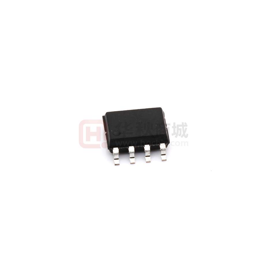
sensor is not affected by external pressure and IC packaging stress. The GT712 is available in SOP8
package, with an operating temperature range of -40~150℃, and complies with RoHS standards.
Main features
Working voltage: 4.5V~5.5V
Static common mode output point: 50% VCC
Wide measuring range: 5A/20A/30A
Isolation voltage: 2500V
High bandwidth: 120kHz
Output response time: 4μs (typical value)
Stability within operating range: 1.5% @ 25℃~150℃; 1% @ -40℃~25℃
Low-noise analog signal path
Strong anti-interference ability
Strong resistance to mechanical stress, magnetic field parametersStrong resistance to mechanical
stress, magnetic field parameters are not shifted by external pressure
ESD (HBM): 5kV
Operating temperature: -40℃~150℃
RoHS certified: (EU) 2015 / 863
Proportional output, bidirectional current
XBLWversion1.0
www.xinboleic.com
Technical support:4009682003
1 / 15
�XBLW GT712
Hall Current Sensor
Application scope
Inverter current detection
Motor phase current detection (motor control)
Photovoltaic inverter
Battery Load Testing System
Current Transformer
Switching Power Supply
Overload Protection Device
Order Information
Product Model
Package Type
GT712LBDTR-05B
SOP-8
GT712LBDTR-20A
GT712LBDTR-20A
XBLWversion1.0
Packing
Packing Qty
GT712LB
05B XXX
XBLW
Tape
3000PCS/Reel
SOP-8
GT712LB
20A XXX
XBLW
Tape
3000PCS/Reel
SOP-8
GT712LB
30A XXX
XBLW
Tape
3000PCS/Reel
www.xinboleic.com
Marking
Technical support:4009682003
2 / 15
�XBLW GT712
Hall Current Sensor
Functional Block Diagra
Pin Information
Name Number
Function
Name
Number
Function
IP+
1
positive current input terminal
GND
5
Ground/Programming Pin
IP+
2
positive current input terminal
TEST
6
Factory Testing/Floating
IP-
3
negative current input terminal
OUT
7
Signal Output/Programming Pin
IP-
4
negative current input terminal
VCC
8
Power Supply/Programming Pin
XBLWversion1.0
www.xinboleic.com
Technical support:4009682003
3 / 15
�XBLW GT712
Hall Current Sensor
Limiting Parameter
Using the device beyond its limiting parameters may cause instability of the chip's functions, and
prolonged exposure to such conditions may damage the chip.
Symbol
Parameter
Minimum value
Power supply voltage
VCC
Output voltage
VOUT
Output current source
IOUT (source)
Output current sink
IOUT (sink)
Working Environment Temperature
TA
Storage Temperature
TS
Maximum Junction Temperature
TJ
Endurance
EEPROM Programming cycle number
Transient surge
current at current
sampling terminal
Maximum value
Unit
-
6
V
-
VCC-0.5
V
-
80
mA
-
40
mA
-40
150
℃
-65
170
℃
-
165
℃
200
-
IP1pulse100ms
cycle
100
A
Electrostatic Discharge(ESD) parameters
Symbol
VESD
Human Body
Model (HBM)
XBLWversion1.0
Execution Standard
Maximum Value
Unit
JEDECJS-001-2017
5
kV
www.xinboleic.com
Technical support:4009682003
4 / 15
�XBLW GT712
Hall Current Sensor
Electrical parameters
Symbol
VCC
Parameter
Test conditions
Minimum
value
-
4.5
5
5.5
V
Operating voltage
Typical Maximum
Unit
value
value
ICC
Operating current
TA=25℃, Output No Load
9
11.18
13
mA
BW
Built-in bandwidth
Smallsignal: –3dB, CL=1nF,
TA=25℃
-
120
-
KHz
TPO
TTC
TA=25℃, CL=1nF, Sensitivity
2mV/G, Constant Magnetic Field:
400Gs
Power-on time
Temperaturecompensated power-on
time
VUVLOH
Undervoltage lockout
threshold
VUVLOL
VPORH
Reset voltage
VPORL
tPORR
ISCLP
Power-on reset release
time
TA=150℃, CL=1nF, Sensitivity
2mV/G, Constant Magnetic Field:
400Gs
100
-
-
us
TA=25℃, Voltage rises, Device starts
operating.
4.1
V
TA=25℃, Voltage drops, Device stops
operating.
3.8
V
TA=25℃, VCC rises.
-
4.1
-
V
TA=25℃,VCC drops.
-
3.8
-
V
TA=25℃,VCC rises.
-
10
-
us
Maximum current source
80
ISCLN
Maximum sink current
-
VOL
Analog output saturation
low level
RL>=4.7KΩ
VOH
Analog output saturation
high level
RL>=4.7KΩ
XBLWversion1.0
300
us
www.xinboleic.com
-
40
mA
-
0.5
VCC-0.3
Technical support:4009682003
-
mA
V
4.97
V
5 / 15
�XBLW GT712
Hall Current Sensor
CL
RL
ROUT
Output load capacitance
VOUTtoGND
Output load resistance
0.5
1
nF
VOUTtoGND
10
-
KΩ
VOUTtoVCC
10
KΩ
-
9
Ω
Output resistance
-
Rise time
TA=25°C, constant magnetic field
400Gs, CL=1nF, sensitivity 2mV/Gs.
Transmission delay
TA=25°C, constant magnetic field
400Gs, CL=1nF, sensitivity 2mV/Gs.
Response time
TA=25°C, constant magnetic field
400Gs, CL=1nF, sensitivity 2mV/Gs.
-
4
5
us
VN
Noise
TA=25°C, CL=1nF, sensitivity 2mV/Gs,
BWf=Bwi.
-
14.1
-
mVp-p
RP
Main Current End
Resistance
1.5
1.8
mΩ
Elin
Linear Error
TA=25°C, CL=1nF, sensitivity 2mV/Gs,
BWf=Bwi.
-
0.4
Voq
Quiescent Point
TA=25°C, CL=1nF, sensitivity 2mV/Gs,
BWf=Bwi.
2.485
2.500
tR
TPD
TRESP
XBLWversion1.0
www.xinboleic.com
-
5.5
-
4.5
Technical support:4009682003
us
us
%
2.515
V
6 / 15
�XBLW GT712
Hall Current Sensor
Accuracy parameter
GT712LBDTR-05B
Parameter.
Condition
Symbol.
current range
IP
Zero Current Output
Temperature Coefficient ΔVOUT(Q)
Total Output Error
ETOT
Output Noise
VNOISE(PP)
Sensitivity
Sensitivity Temperature
Coefficient
Unit
±5
A
0.26
mV/℃
-3.0
3.0
46
ΔSens
Full Current Range
TA=150°C, TA=40°C relative to 25°C
Parameter
Symbol
Condition
Current Range
IP
Sens
Minimum Typical Maximum
value
value
value
180
185
%
mV
190
mV/A
0
%/℃
Minimum Typical Maximum
value
value
value
Unit
GT712LBDTR-20A
-20
Zero Current Output
Temperature Coefficient ΔVOUT(Q)
20
0.26
Total Output Error
ETOT
Output Noise
VNOISE(PP)
Sensitivity
Sensitivity Temperature
Coefficient
Sens
ΔSens
XBLWversion1.0
www.xinboleic.com
-3.0
mV/℃
3.0
30
Full Current Range
TA=150°C, TA=-40°C
relative to 25°C
96
100
0
Technical support:4009682003
A
%
mV
104
mV/A
%/℃
7 / 15
�XBLW GT712
Hall Current Sensor
GT712LBDTR-30A
Parameter
Symbol
Current Range
IP
Condition
Minimum Typical Maximum
value
value
value
-30
Zero Current Output
Temperature Coefficient ΔVOUT(Q)
30
0.26
Total Output Error
ETOT
Sensitivity
Sens
Full Current Range
Thermal coefficient of
sensitivity
ΔSens
TA=150℃, TA=-40℃
, relative to 25℃
Output Noise
VNOISE(PP)
-3.0
64
66.6
Unit
A
mV/℃
3.0
%
69
mV/A
0
%/℃
20
mV
Feature definition
1.Power-on Time - TPO
Power-on time: The time taken for the power supply to reach thePower-on time: The time taken for the
power supply to reach the minimum operating voltage VCCM IN is t1; the time taken for the output to
reach 90% of its steady value under an external magnetic field is t2. The difference between these two
times is the power-on time.
Figure 1: Definition of Power-on Time
XBLWversion1.0
www.xinboleic.com
Technical support:4009682003
8 / 15
�XBLW GT712
Hall Current Sensor
2.Temperature Compensated Power-on Time - TTC
After power-on, temperature trimming time is required before valid temperature compensation output.
3.Transmission Delay - TPD
The time difference between the output reaching 20% of its final value when the external magnetic field
reaches 20% of its final value.
4.Rise time - TR
The time difference between the rise of the chip output level from 10% to 90%.
Figure 3: Definition of Rise Time
XBLWversion1.0
www.xinboleic.com
Technical support:4009682003
9 / 15
�XBLW GT712
Hall Current Sensor
5. Response Time - TRESP
The time difference between when the external magnetic field applied to the chip reaches 80% of its
final value and when the corresponding output value also reaches 80%.
6. Static Voltage Output - VOQ
Under the condition that the power supply voltage of the chip and the ambient temperature are within
the operating range, and the measured current is 0, the output of the chip is...
Note: Prolonged operation at the maximum rated value may affect the reliability of the device.
Exceeding the maximum rated value may damage the device.
7. Static Voltage Output Error - VOE
The difference between the actual output voltage of the sensor and the ideal output voltage power supply
when the measured current value is zero. In proportional output mode with power supply, the static
voltage output error is the difference between the actual output error and VCC / 2.
8. Sensitivity
Sensitivity indicates the change value of sensor output per 1A change of measured current, with the unit
of mV/A. The calculation method is to pass through the positive full-scale current and negative fullscale current, and divide the difference between the output voltage at 2 points of the sensor by the
difference between the positive full-scale current and negative full-scale current, which is the sensitivity
of the sensor. The specific calculation formula is as follows:
SENS = (Vout(IPma0) − Vout(Inma0))/(IPma0 − Inma0)
Here, IPma0 and Inma0 are the positive full-scale current and negative full-scale current respectively,
Vout(IPma0) and Vout(Inma0) are the analog output voltages of the sensor when passing through the
positive full-scale current and negative full-scale current respectively.
XBLWversion1.0
www.xinboleic.com
Technical support:4009682003
10 / 15
�XBLW GT712
Hall Current Sensor
9. Global Error Budget - ETOT
This error value represents the maximum error of the sensor under various environmental conditions,
which is equal to the absolute value of the measurement error within each temperature range, divided by
the maximum output dynamic range of the sensor, over the full current measurement range. It can be
expressed as follows:
ETOT(IP)=Ma0(Vout –Vout_ idea)/(Vout(IPma0)-Voq)
Here, Ma0 (Vout – Vout _ idea) represents the maximum error within the measurementHere, Ma0 (Vout
– Vout _ idea) represents the maximum error within the measurement range and (Vout (IPma0) -Voq)
represents the maximum output dynamic range of the sensor.
10. Non-linearity error - ELIN
Due to the non-ideal characteristics of the sensor, the output voltageDue to the non-ideal characteristics
of the sensor, the output voltage is not completely linear with the measured current in practical
applications. After linear fitting by least squares method, the linearity error of the sensor can be obtained
by dividing the maximum output error of the sensor by its dynamic range, i.e. ELIN (IP) = ∆Vout /
(Vout (IPma0) -Voq). Here, ∆Vout is the maximum linearity error within the measuring range of the
sensor.
XBLWversion1.0
www.xinboleic.com
Technical support:4009682003
11 / 15
�XBLW GT712
Hall Current Sensor
Characteristic curve
XBLWversion1.0
www.xinboleic.com
Technical support:4009682003
12 / 15
�XBLW GT712
Hall Current Sensor
Typical Application Circuit
The typical application circuit of GT712 includes a filter capacitor CVcc between VCC and ground, as
well as an optional filter capacitor CVout between the output and ground. At the input end of the
measured current, pins 1 and 2 are shorted together to serve as the input end of the measured current,
while pins 3 and 4 are shorted together to serve as the output end of the measured current. The analog
output signal of the sensor is perfectly proportional to the AC/DC current being measured.
Typical application circuit
3-Phase Motor Control Application Circuit
XBLWversion1.0
www.xinboleic.com
Technical support:4009682003
13 / 15
�XBLW GT712
Hall Current Sensor
Encapsulate data
Dimensions (mm)
Symbol
A
A1
A2
b
c
D
e
E
E1
L
θ
XBLWversion1.0
Minimum value
Dimensions (inches)
Maximum value
1.350
0.100
1.350
0.330
0.170
4.800
1.750
0.250
1.550
0.510
0.250
5.000
1.270(BSC)
5.800
6.200
3.800
4.000
0.400
1.270
0°
8°
www.xinboleic.com
Minimum value
Maximum value
0.530
0.004
0.053
0.013
0.007
0.189
0.069
0.010
0.061
0.020
0.010
0.197
0.050(BSC)
0.228
0.150
0.016
0°
Technical support:4009682003
0.224
0.157
0.050
8°
14 / 15
�XBLW GT712
Hall Current Sensor
Declaration
Shenzhen Xinbole Electronics Co., Ltd. reserves the right to modify the product manual without prior
notice! Customers are advised to confirm if the information received is the latest version and verify the
completeness of related information before placing an order.
Under certain conditions, any semiconductor product may fail or malfunction. It is the buyer's
responsibility to comply with safety standards and take appropriate safety measures when designing
systems and manufacturing complete machines using products from Shenzhen Xinbole Electronics Co.,
Ltd. to avoid potential risks of failure that may cause personal injury or property damage.
This document is for reference only, and the actual use should be based on the application test results.
Product performance improvement is endless. Shenzhen Xinbole Electronics Co., Ltd. will sincerely
provide customers with integrated circuit products with better performance and higher quality.
XBLWversion1.0
www.xinboleic.com
Technical support:4009682003
15 / 15
�


 工商网监
湘ICP备2023018690号
工商网监
湘ICP备2023018690号
