TM
CaliPile
Infrared Sensing Solu�ons
TPiS 1S 1385 / 5029
Product Specifica�on
Features
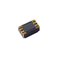
• 4.4 × 2.6 × 1.75 mm3 ceramic
SMD package
• High sensitivity thermopile with
120◦ field-of-view
• Integrated 50 µW low-power signal processing
• I2 C
interface,
hardwareconfigurable address
• Calibration data for ambient and
object temperature sensing
• Interrupt function for presence,
motion, over-temperature and
more
Applications
• Optimal to wake-up battery opThe TPiS 1S 1385 is the most compact thermopile sensor with integrated signal
TM
processing within the CaliPile product range. It features a wide field of view
and a low power consumption. The technology of a high sensitive thermopile
combined with a smart data treatment allows for much more than the traditional temperature measurement of remote objects. Once configured via the
I2 C interface an interrupt output can be used to monitor motion, presence or
an over-temperature of remote objects.
One typical application are very thin battery operated devices which have to
be waked-up only when presence of a human has been discovered in a small
distance of up to 3 m. The whole device can be designed very thin since no
optical components such as Fresnel-lenses are required for that application.
erated thin devices
• Near-field
human
presence
sensing
• Far-field human motion detection (with lens)
• Short-range temperature measurement
• Fast remote over-temperature
protection
�Contents
1 Dimensions and Connections
3
2 Optical Characteristics
4
3 Absolute Maximum Ratings
5
4 Device Characteristics
5
5 I2 C Interface Characteristics
5.1 START and STOP conditions . .
5.2 Clock low extension . . . . . .
5.3 Slave Address . . . . . . . . .
5.4 Protocol diagram description .
5.5 General Call . . . . . . . . . .
5.6 Reading Data from the Register
5.7 Writing Data to Register . . . .
5.8 Reading EEPROM . . . . . . .
.
.
.
.
.
.
.
.
.
.
.
.
.
.
.
.
.
.
.
.
.
.
.
.
.
.
.
.
.
.
.
.
.
.
.
.
.
.
.
.
.
.
.
.
.
.
.
.
.
.
.
.
.
.
.
.
.
.
.
.
.
.
.
.
.
.
.
.
.
.
.
.
.
.
.
.
.
.
.
.
.
.
.
.
.
.
.
.
.
.
.
.
.
.
.
.
.
.
.
.
.
.
.
.
.
.
.
.
.
.
.
.
.
.
.
.
.
.
.
.
.
.
.
.
.
.
.
.
.
.
.
.
.
.
.
.
.
.
.
.
.
.
.
.
.
.
.
.
.
.
.
.
.
.
.
.
.
.
.
.
.
.
.
.
.
.
.
.
.
.
.
.
.
.
.
.
.
.
.
.
.
.
.
.
.
.
.
.
.
.
.
.
.
.
.
.
.
.
.
.
.
.
.
.
.
.
.
.
.
.
.
.
.
.
.
.
.
.
.
.
.
.
.
.
.
.
.
.
.
.
.
.
.
.
.
.
.
.
.
.
.
.
.
.
.
.
.
.
.
.
.
.
.
.
.
.
.
.
.
.
.
.
.
.
.
.
.
.
.
.
.
.
.
.
.
.
.
.
.
.
.
.
.
.
.
.
.
.
7
7
8
8
8
8
9
9
10
6 Data processing characteristics
11
6.1 Control and Status Registers . . . . . . . . . . . . . . . . . . . . . . . . . . . . . . . . . . . . . 11
6.2 Control Register Details . . . . . . . . . . . . . . . . . . . . . . . . . . . . . . . . . . . . . . . . 12
7 Internal processing overview
7.1 Object and Ambient Temperatures . . . . . . . .
7.2 Presence detection . . . . . . . . . . . . . . . .
7.3 Motion detection . . . . . . . . . . . . . . . . .
7.4 Ambient temperature shock detection . . . . . .
7.5 Object temperature over or under limit detection
7.6 Hysteresis . . . . . . . . . . . . . . . . . . . . .
.
.
.
.
.
.
.
.
.
.
.
.
.
.
.
.
.
.
.
.
.
.
.
.
.
.
.
.
.
.
.
.
.
.
.
.
.
.
.
.
.
.
.
.
.
.
.
.
.
.
.
.
.
.
.
.
.
.
.
.
.
.
.
.
.
.
.
.
.
.
.
.
.
.
.
.
.
.
.
.
.
.
.
.
.
.
.
.
.
.
.
.
.
.
.
.
.
.
.
.
.
.
.
.
.
.
.
.
.
.
.
.
.
.
.
.
.
.
.
.
.
.
.
.
.
.
.
.
.
.
.
.
.
.
.
.
.
.
.
.
.
.
.
.
.
.
.
.
.
.
.
.
.
.
.
.
16
16
16
17
18
19
19
8 Temperature Measurement
8.1 EEPROM content . . . . . . . . . . . .
8.2 EEPROM Details . . . . . . . . . . . . .
8.3 Calculation of the Ambient Temperature
8.4 Calculation of the Object Temperature .
.
.
.
.
.
.
.
.
.
.
.
.
.
.
.
.
.
.
.
.
.
.
.
.
.
.
.
.
.
.
.
.
.
.
.
.
.
.
.
.
.
.
.
.
.
.
.
.
.
.
.
.
.
.
.
.
.
.
.
.
.
.
.
.
.
.
.
.
.
.
.
.
.
.
.
.
.
.
.
.
.
.
.
.
.
.
.
.
.
.
.
.
.
.
.
.
.
.
.
.
.
.
.
.
.
.
.
.
.
.
.
.
.
.
.
.
20
20
20
21
22
9 Integration instructions and recommendations
9.1 Position . . . . . . . . . . . . . . . . . . . .
9.2 Wiring patterns . . . . . . . . . . . . . . . .
9.3 Footprint . . . . . . . . . . . . . . . . . . .
9.4 Re-flow soldering . . . . . . . . . . . . . . .
.
.
.
.
.
.
.
.
.
.
.
.
.
.
.
.
.
.
.
.
.
.
.
.
.
.
.
.
.
.
.
.
.
.
.
.
.
.
.
.
.
.
.
.
.
.
.
.
.
.
.
.
.
.
.
.
.
.
.
.
.
.
.
.
.
.
.
.
.
.
.
.
.
.
.
.
.
.
.
.
.
.
.
.
.
.
.
.
.
.
.
.
.
.
.
.
.
.
.
.
.
.
.
.
.
.
.
.
.
.
.
.
23
23
23
23
23
.
.
.
.
.
.
.
.
10 Packaging Specification
25
10.1 General Information . . . . . . . . . . . . . . . . . . . . . . . . . . . . . . . . . . . . . . . . . 25
10.2 Carrier Tape . . . . . . . . . . . . . . . . . . . . . . . . . . . . . . . . . . . . . . . . . . . . . . 25
11 Statements
11.1 Patents . . .
11.2 Quality . . .
11.3 RoHS . . . .
11.4 Liability Policy
11.5 Copyright . .
.
.
.
.
.
.
.
.
.
.
.
.
.
.
.
.
.
.
.
.
.
.
.
.
.
.
.
.
.
.
.
.
.
.
.
.
.
.
.
.
.
.
.
.
.
.
.
.
.
.
.
.
.
.
.
.
.
.
.
.
.
.
.
.
.
.
.
.
.
.
.
.
.
.
.
.
.
.
.
.
.
.
.
.
.
.
.
.
.
.
.
.
.
.
.
.
.
.
.
.
.
.
.
.
.
.
.
.
.
.
.
.
.
.
.
.
.
.
.
.
.
.
.
.
.
.
.
.
.
.
.
.
.
.
.
.
.
.
.
.
.
.
.
.
.
.
.
.
.
.
.
.
.
.
.
.
.
.
.
.
.
.
.
.
.
.
.
.
.
.
.
.
.
.
.
.
.
.
.
.
.
.
.
.
.
.
.
.
.
.
.
.
.
.
.
.
.
.
.
.
.
.
.
.
.
.
.
.
.
.
.
.
.
.
.
.
.
.
.
.
.
.
.
.
.
27
27
27
27
27
27
�TPiS 1S 1385 / 5029
Dimensions and Connections
Figure 1: Mechanical Dimensions (in mm). The active pixel size A is 0.56 × 0.56 mm2 .
4,4 ` 0,15
1,75 +- 0,25
0,2
0,75
Indexmark (0,25SQ)
Gloptop
0,4 ` 0,05
2,5 ` 0,1
0,4(2x)
0,45 ` 0,15
1,55
0,25(4x)
3,3 ` 0,1
0,33Optical Distance
A
0,9
The optical distance in figure 1 is the effective distance between the chip active area and the filter top taking
into account the refraction in the optical light path.
Figure 2: Pin Configuration. A short description is given in table 1.
INT
SCL
A0
A1
A0
A1
INT
SCL
SDA
VDD
VSS
VSS
VSS
VSS
SDA
VDD
Table 1: Pin descriptions. Further explanations follow in this document.
Pin Symbol
Pin Name and short Functional Description.
Pin Type
A0,A1
Address Inputs A0, A1: Setting the last 2 bits of the slave address. Setting a
pin to GND corresponds to 0. Setting a pin to VDD corresponds to a 1. The
device address with both pins set to GND is 0xC.
Input
VSS
Ground: The ground (GND) reference for the power supply should be set to
the host ground.
Power
VDD
Power Supply: The power supply for the device. Typical operating voltage is
3.3 V
Power
SDA
Serial Data: The I2 C bidirectional data line. Open-drain driven and requires
pull-up resistors to min. 1.8 V
Input/Output
SCL
Serial Clock Input: The I2 C clock input for the data line. Up to 400 kHz are
possible. The host must support clock stretching.
Input/Output
INT
Interrupt Output: The open drain / active low Interrupt output to indicate a
detected event. Reading the chip register out resets this output.
Output
3
Excelitas Technologies GmbH & Co. KG
Wenzel-Jaksch-Str. 31
65199 Wiesbaden Germany
Tel.: +49 (0)611 492 0
Fax.: +49 (0) 611 492 177
www.excelitas.com
Product Specification
1
18/11/2016- Preliminary
�TPiS 1S 1385 / 5029
Product Specification
2
18/11/2016- Preliminary
Optical Characteristics
Table 2: Optical characteristics
Parameter
Field of View
Symbol
Min
Typ
−10
120
0
FOV
Optical Axis
Max
Unit
Remarks / Conditions
at 50 % intensity
◦
10
◦
Figure 3: Typical FoV measurement-result
Relative Signal [a. u.]
1,00
0,90
0,80
0,70
0,60
0,50
0,40
0,30
0,20
0,10
0,00
-90 -80 -70 -60 -50 -40 -30 -20 -10 0 10 20 30 40 50 60 70 80 90
Angle of Incidence [degree]
Table 3: Filter properties
Parameter
Symbol
Min
Typ
Average Filter Transmittance
TA
TA
λ (5 %)
75
>77
5.2
5.5
Average Filter Transmittance
Cut-on Wavelength
Max
99 %
The TPiS 1S 1385 temperature measurement is specified for a full field-of-view coverage by a black body with
more than 99 % emissivity.
Table 7: Ambient temperature sensor (PTAT)
Parameter
Symbol
Min
Slope
Range
Linearity
Offset
Noise(peak-peak)
Typ
15
170
Resolution
−20
−5
11 000
13 500
5
Max
Unit
Remarks / Conditions
Bits
counts/K
90
5
16 000
−20 ◦C to 85 ◦C
◦C
%
−20 ◦C to 85 ◦C
counts
counts
5
Excelitas Technologies GmbH & Co. KG
Wenzel-Jaksch-Str. 31
65199 Wiesbaden Germany
Tel.: +49 (0)611 492 0
Fax.: +49 (0) 611 492 177
www.excelitas.com
Product Specification
3
18/11/2016- Preliminary
�TPiS 1S 1385 / 5029
18/11/2016- Preliminary
Product Specification
Figure 5: Typical temperature dependence of the raw thermopile output
200
U=130000 counts
U=120000 counts
U=110000 counts
U=100000 counts
U= 90000 counts
U= 80000 counts
U= 70000 counts
U= 60000 counts
U= 50000 counts
U= 40000 counts
U= 30000 counts
U= 20000 counts
U= 10000 counts
U= 0 counts
150
100
Tobj[°C]
50
0
-50
-100
-150
-200
-250
-50
0
50
100
150
200
Tamb[°C]
Figure 5 shows calculated thermopile raw data U = TPobject as a function of the ambient temperature and
object temperature based on typical characteristics of TPiS 1S 1385 . The ASIC typically features a wider dynamic
range as compared to the specified values in table 6 and 7. Values out of our specifications are not guaranteed.
The calculation of a temperature has to be performed on the host system and is described in section 8.
Table 8: Digital Interface (SCL, SDA, INT, A0, A1)
Parameter
Symbol
Min
Typ
Max
Unit
Input low voltage
VI L
VI H
VO L
VO H
I LI
I LO
FS C L
TH I G H
TLOW
-
-
V
1.5
0.2
0.6
-
-
V
-
-
V
VI 2C
1
1
400
Input high voltage
Output low voltage
Output high voltage
Input leakage current
Output leakage current
SCL Frequency
SCL high time
SCL low time
refresh time
-
-
−1
-
-
-
-
-
200
0.2
-
-
ns
-
µs
-
-
90*
3
Remarks / Conditions
V
Open Drain
µA
VI = VD D /2
VO = VD D
µA
kHz
*Slave clock stretching
ms
6
Excelitas Technologies GmbH & Co. KG
Wenzel-Jaksch-Str. 31
65199 Wiesbaden Germany
Tel.: +49 (0)611 492 0
Fax.: +49 (0) 611 492 177
www.excelitas.com
�TPiS 1S 1385 / 5029
I2 C Interface Characteristics
An I2 C serial interface is provided to read out the sensors data and for read and write access of configuration and
status registers and to obtain calibration data from the EEPROM.
TM
The following chapters give detailed instructions to understand and to operate the I2 C interface of the CaliPile .
For the complete I2 C specifications (version 2.1) refer to: www.i2c-bus.org.
The SCL is a bidirectional input and output used as synchronization clock for serial communication. The SDA
is a bidirectional data input and output for serial communication. The SCL and SDA outputs operate as open drain
outputs only. External pull-up resistors are required. The pull-up resistor does all the work of driving the signal
line high. All devices attached to the bus may only drive the SDA and SCL lines low.
TM
The I2 C interface allows connection of a master device (MD) and one or more slave devices (SD). The CaliPile can
be operated as a SD only. The MD provides the clock signals and initiates the communication transfer by selecting
a SD through a slave address (SA) and only the SD, which recognizes the SA should acknowledge (ACK), the rest of
SDs should remain silent.
The general data transfer format is illustrated in figure 6
Figure 6: Illustration of voltages during I2 C communication
SDA
SCL
1-7
S
8
slave addr
9
1-7
8
9
ACK
ACK
1-7
8
9
ACK
DATA
P
Start Condition
S
R/Wv
TN)ACK
P
5.1
Read = 1 / Writev = 0
TNot) Acknowledge; ACK = 0 , NACK = 1
Stop Condition
START and STOP conditions
Figure 7: START and STOP Condition
SDA
SCL
S
P
START condition
STOP condition
Two unique bus situations define a message START and STOP condition which is shown in figure 7.
1. A high to low transition of the SDAT line while SCLK is high indicates a message START condition.
2. A low to high transition of the SDAT line while SCLK is high defines a message STOP condition. START and
STOP conditions are always generated by the bus master. After a START condition the bus is considered to
be busy. The bus becomes idle again after certain time following a STOP condition or after both the SCLK
and SDAT lines remain high for more than tHIGH:MAX .
7
Excelitas Technologies GmbH & Co. KG
Wenzel-Jaksch-Str. 31
65199 Wiesbaden Germany
Tel.: +49 (0)611 492 0
Fax.: +49 (0) 611 492 177
www.excelitas.com
Product Specification
5
18/11/2016- Preliminary
�TPiS 1S 1385 / 5029
Product Specification
5.2
18/11/2016- Preliminary
Clock low extension
Figure 8: Clock low extension
TLOW = 90μs max.
SDA
SCL
Low extension
TM
The CaliPile may need some time to process received data or may not be ready yet to send the next byte.
In this case the SD can pull the SCL clock low to extend the low period of SCL and to signal to the master that it
should wait (see figure 8). Once the clock is released the master can proceed with the next byte.
5.3
Slave Address
TM
After power up the CaliPile responds to the General Call Address (0x00) only. Upon receipt of a general call, it
loads its slave address from EEPROM (ESA). The slave address stored in the EEPROM consists of 7 address
bits (6:0) and 1 address control bit (7). If the address control bit is set, the slave address read from the EEPROM
is merged with the information from the slave address select pins A1 and A0.
Table 9: Examples for the interplay between configuration pins and the EEPROM
ESA
state
I2 C slave address
1000 1111
H:L
000 1110
1000 1100
H:L
000 1110
1000 1100
L:H
000 1101
0000 1100
L:H
000 1100
1ABC DEFG
Y:Z
ABC DEYZ
0ABC DEFG
Y:Z
ABC DEFG
TM
Some examples are given in table 9. The CaliPile in the standard configuration has enabled configuration
pins. The standard EEPROM content is 1000 1100. The standard slave address is therefore dec12 or 000 1100 in
binary representation when the address input pins A1,A0 are both connected to ground. Pulling A0 to a high level
for example will result in the slave address dec13 or 000 1101.
5.4
Protocol diagram description
In the following chapters, the communication protocol will be illustrated with diagrams. Figure 9 describes the
meaning of those diagrams.
5.5
General Call
In order to re-fresh the slave address from EEPROM the MD has to send a general call (0x00) followed by the reload
command (0x04). The slave may require up to 300 µs for copying the slave address from EEPROM information
into the register.
8
Excelitas Technologies GmbH & Co. KG
Wenzel-Jaksch-Str. 31
65199 Wiesbaden Germany
Tel.: +49 (0)611 492 0
Fax.: +49 (0) 611 492 177
www.excelitas.com
�TPiS 1S 1385 / 5029
18/11/2016- Preliminary
Product Specification
Figure 9: Protocol diagram description
1
8
1
Register Address
A
1
7
1
S
Slave Address
S
Rd
Wr
A
A
P
Start Condition
Read 8bit value of 1)
Write 8bit value of 0)
ACK = Acknowledge 8bit value of 0)
NACK = Not Acknowledge 8bit value of 1)
Stop Condition
Rd A
8
Data Byte
1
1
A
P
Master-to-Slave
Slave-to-Master
Continuation of Protocoll
…
Figure 10: General call format
5.6
1
7
S
0x00
1
1
Wr A
Rd
8
1
1
0x04
A
P
Reading Data from the Register
Each register can be read through the I2 C bus interface. The address information following Slave address points
to the register to be read. The SD may require some time to load the data into the serial interface and therefore
apply "clock stretching" after reception of the address byte. Once the data is ready for transmission to the MD,
clock-stretching will be released and the MD can clock out the data byte.
The address pointer on the SD will be automatically incremented to prepare for the next data byte to be
fetched for transmission. The SD may apply "clock stretching" again to enforce a waiting time, before the next
data byte is ready for transmission. The address pointer will wrap around to 0 once it exceeds address 63.
Reading of data can be interrupted by the MD at any time by generating a stop or a new start condition or a
"not acknowledge". This is illustrated in figure 11.
Figure 11: Register read format
1
S
5.7
7
1
Slave Address
8
1
1
7
Register Address
A
Sr
Slave Address
1
Wr A
1
1
Rd A
8
1
Data [Adr]
A
8
1
8
1
8
1
8
1
1
Data [Adr+1]
A
Data [Adr+2]
A
Data [Adr+N-1]
A
Data [Adr+N]
A
P
Writing Data to Register
Each register can be written to through the I2 C bus interface. The address information following the Slave address
specifies the location, where the next data byte is written to. The SD may require some time to write the data
into the registers on chip and therefore apply "clock stretching" after reception of the data byte. Once the data
is stored in the register, the slave will increment the address pointer and prepare for the next data byte to be
received. The address pointer will wrap around when it exceeds 63.
Writing of data can be interrupted at any time by generating a stop or a new start condition or a "not acknowledge". This is illustrated in figure 12.
If the address points to a non-writable register, the register content remains unchanged.
9
Excelitas Technologies GmbH & Co. KG
Wenzel-Jaksch-Str. 31
65199 Wiesbaden Germany
Tel.: +49 (0)611 492 0
Fax.: +49 (0) 611 492 177
www.excelitas.com
�TPiS 1S 1385 / 5029
18/11/2016- Preliminary
1
S
5.8
7
1
Slave Address
8
1
8
1
Register Address
A
Data [Adr]
A
1
Wr A
8
1
Data [Adr+1]
A
8
1
8
1
8
1
8
1
1
Data [Adr+2]
A
Data [Adr+3]
A
Data [Adr+N-1]
A
Data [Adr+N]
A
P
Reading EEPROM
A dedicated EEPROM control register (ECR) is provided to control access mode and to allow testing of EEPROM during production. Prior to reading EEPROM memory via I2C interface the control byte needs to be set accordingly.
It is of importance to configure the EEPROM control register correctly as specified to ensure correct operation. In
order to enable EEPROM reading, the ECR must be set to 0x80 as depicted in figure 13.
Figure 13: Configuring register for EEPROM readout
1
7
S
1
Slave Address
1
Wr A
8
8
1
Reg. Address (0x1F)
A
1
ECR (0x80)
1
P
A
Note: Configuring the ECR for EEPROM read access causes increase of the supply current during EEPROM
read operation until ECR will be set to 0x00 again.
Once the ECR has been setup correctly for read operation, the EEPROM cells can be addressed and read as
drawn to figure 14.
Figure 14: Reading EEPROM
1
S
1
7
Slave Address
8
1
1
7
1 1
8
1
Register Address
A
Sr
Slave Address
Rd A
Data [Adr]
A
1
Wr A
8
1
8
1
8
1
8
1
1
Data [Adr+1]
A
Data [Adr+2]
A
Data [Adr+N-1]
A
Data [Adr+N]
A
P
The address information following the Slave address points to the EEPROM memory location to be read. The
SD may require some time to load the data into the serial interface and therefore apply "clock stretching" after
reception of the address byte. Once the data is ready for transmission to the MD, clock stretching will be released
and the MD can clock out the data byte.
The address pointer on the SD will be automatically incremented to prepare for the next data byte to be
fetched for transmission. The SD may apply "clock stretching" again to enforce a waiting time, before the next
data byte is ready for transmission. The address pointer will wrap around to 0 once it exceeds address 63.
The EEPROM control register must be configured to 0x00 after the end of the EEPROM read operation to bring
the supply current back to normal (lower) level.
10
Excelitas Technologies GmbH & Co. KG
Wenzel-Jaksch-Str. 31
65199 Wiesbaden Germany
Tel.: +49 (0)611 492 0
Fax.: +49 (0) 611 492 177
www.excelitas.com
Product Specification
Figure 12: Register write format
�TPiS 1S 1385 / 5029
Data processing characteristics
6.1
Control and Status Registers
Table 10: Register content
Register #
Size[bit]
Access
reserved
8
-
1-2,3[7]
TPobject
17
Read
3[6:0],4
TPambient
15
Read
5-7[7:4]
TPObjLP1
20
Read
7[3:0]-9
TPObjLP2
20
Read
10-11
TPambLP3
16
Read
12-14
0
Description
TPObjLP2 frozen
24
Read
15
TPpresence
8
Read
16
TPmotion
8
Read
17
TPamb shock
8
Read
18[7:0]
Interrupt Status
8
Read(Autoclear)
19[7:0]
Chip Status
8
Read
20[3:0]
SLP1
4
Write/Read
20[7:4]
SLP2
4
Write/Read
21[3:0]
SLP3
4
Write/Read
21[7:4]
reserved
4
-
22
TPpresence threshold
8
Write/Read
23
TPmotion threshold
8
Write/Read
24
TPamb shock threshold
8
Write/Read
25[4:0]
Interrupt Mask Register
5
Write/Read
25[7:5]
reserved
3
-
26[1:0]
Cycle time for Motion differentiation
2
Write/Read
26[3:2]
SRC select for presence determination
2
Write/Read
TPOT direction
1
Write/Read
26[7:5]
reserved
3
-
27[7:0]
Timer interrupt
8
Write/Read
28,29
26[4]
TPOT threshold
16
Write/Read
30
reserved
8
-
31
EEPROM control
8
Write/Read
62:32
EEPROM content
248
Read
8
Read
63
Slave address
TM
The control and status registers in table 10 give access to the variables of the integrated CaliPile ASIC. Details
on the registers are given in the following section 6.2.
While some registers contain computed values other contain parameters to control the functionality of the
chip which is described in section 7.
The register control values are undefined after power-up and require an initialization procedure for
TM
a well-defined operation of the CaliPile .
11
Excelitas Technologies GmbH & Co. KG
Wenzel-Jaksch-Str. 31
65199 Wiesbaden Germany
Tel.: +49 (0)611 492 0
Fax.: +49 (0) 611 492 177
www.excelitas.com
Product Specification
6
18/11/2016- Preliminary
�TPiS 1S 1385 / 5029
Control Register Details
TPobject
Register #1[7:0]
7
6
5
4
3
2
Register #2[7:0]
1
0
7
6
5
4
3
2
Register #3[7]
1
0
7
-
-
-
-
-
-
-
Contains the 17 bit TPobject raw ADC value in digits. This represents the current signal of the thermopile sensor
element.
TPambient
Register #3[6:0]
-
6
5
4
3
Register #4[7:0]
2
1
0
7
6
5
4
3
2
1
0
Contains the 15 bit TPambient raw value in digits. This represents the current signal of the ambient temperature
sensor (PTAT).
TPobjectLP1
Register #5[7:0]
7
6
5
4
3
2
Register #6[7:0]
1
0
7
6
5
4
3
2
Register #7[7:4]
1
0
7
6
5
4
-
-
-
-
Contains the 20 bit TPobjLP1 value in digits. This represents the low-pass-filtered value of the TPobject signal. To
compare it with the 17 bit wide TPobject divide the value by 23 = 8. The filter time constant for this filter stage can
be set with SLP1 .
TPobjectLP2
Register #7[3:0]
-
-
-
-
3
2
Register #8[7:0]
1
0
7
6
5
4
3
2
Register #9[7:0]
1
0
7
6
5
4
3
2
1
0
Contains the 20 bit TPobjLP2 value in digits. This represents the low-pass-filtered value of the TPobject signal. To
compare it with the 17 bit wide TPobject divide the value by 23 = 8. The filter time constant for this filter stage can
be set with SLP2 .
TPambLP3
Register #10[7:0]
7
6
5
4
3
Register #11[7:0]
2
1
0
7
6
5
4
3
2
1
0
Contains the 16 bit TPambLP3 value in digits. This represents the low-pass-filtered value of the TPambient signal. To
compare it with the 15 bit wide TPambient divide the value by 21 = 2. The filter time constant for this filter stage
can be set with SLP3 .
TPobjectLP2 frozen
Register #12[7:0]
7
6
5
4
3
2
Register #13[7:0]
1
0
7
6
5
4
3
2
Register #14[7:0]
1
0
7
6
5
4
3
2
1
0
Contains the 24 bit TPobjLP2 frozen value in digits. This represents the low-pass-filtered value of the TPobject signal
when motion was detected. To compare it with the 17 bit wide TPobject divide the value by 27 = 128. See
section 7.3 for more details on the motion detection algorithm.
TPpresence
Register #15[7:0]
7
6
5
4
3
2
1
0
Contains the 8 bit TPpresence value in digits. It is the unsigned difference between two values which combination is
steered with the "source select". The sign of the value is contained in the "chip status". See section 7.2 for details.
12
Excelitas Technologies GmbH & Co. KG
Wenzel-Jaksch-Str. 31
65199 Wiesbaden Germany
Tel.: +49 (0)611 492 0
Fax.: +49 (0) 611 492 177
www.excelitas.com
Product Specification
6.2
18/11/2016- Preliminary
�TPiS 1S 1385 / 5029
18/11/2016- Preliminary
Register #16[7:0]
7
6
5
4
3
2
1
0
Contains the 8 bit TPmotion value in digits. It is the unsigned difference between two consecutive values of
TPobjectLP1 . The sign of the value is contained in the "chip status". The interval is steered with the "cycle time". See
section 7.3 for details.
TPamb shock
Register #17[7:0]
7
6
5
4
3
2
1
0
Contains the 8 bit TPamb shock value in digits. It is the unsigned difference between TPambient and TPambL1 . The sign
of the value is contained in the "chip status". See section 7.4 for details.
Interrupt status
Register #18[7:5] sign
Register #18[4:0] flag
7
6
5
4
3
2
1
0
TPpresence
TPmotion
TPamb shock
TPOT
TPpresence
TPmotion
TPamb shock
timer
Each fulfilled interrupt condition between the last readout and the current one is stored here. See also "Chip
status" for the current status of the interrupt conditions. Reading this register clears the register (setting it to
0x00) and resets the physical interrupt output (release to high).
Sign is the sign bit to the corresponding unsigned 8 bit values when the interrupt condition of the corresponding interrupt calculation branches (see section 7) was fulfilled since the last readout of that register. A 0
represents a positive value and a 1 a negative value.
Flag Contains a 1 when a condition of the corresponding interrupt calculation branches was fulfilled since
the last readout of that register.
Timer Contains a 1 when at least one period of the timer passed since the last readout of that register.
Chip status
Register #19[7:5] sign
Register #19[4:0] flag
7
6
5
4
3
2
1
0
TPpresence
TPmotion
TPamb shock
TPOT
TPpresence
TPmotion
TPamb shock
timer
Sign is the sign bit to the corresponding unsigned 8 bit values. A 0 represents a positive value and a 1 a
negative value.
Flag represents the status of the corresponding interrupt calculation branches (see section 7). A 1 represents
a full-filled condition for the interrupt.
Timer represents a flag toggling with the double frequency of the "timer interrupt".
This register is masked by the "Interrupt Mask" register to evaluate the condition for the physical interrupt
TM
output pin at the CaliPile .
Low pass time constants SLP
Register #20[7:4] LP2
7
6
5
Register #20[3:0] LP1
4
3
reserved
-
-
-
2
1
0
Register #21[3:0] LP3
-
3
2
1
0
Contains the time constants for the three low-pass filters LP1, LP2 and LP3 (see section 7). The possible settings
and the corresponding values are denoted in table 11.
13
Excelitas Technologies GmbH & Co. KG
Wenzel-Jaksch-Str. 31
65199 Wiesbaden Germany
Tel.: +49 (0)611 492 0
Fax.: +49 (0) 611 492 177
www.excelitas.com
Product Specification
TPmotion
�TPiS 1S 1385 / 5029
18/11/2016- Preliminary
Product Specification
Table 11: Low pass settings for LP1, LP2 and LP3
fcut off [Hz]
6.4 × 10⁻¹
3.2 × 10⁻¹
1.5 × 10⁻¹
7.9 × 10⁻²
3.9 × 10⁻²
1.9 × 10⁻²
9.9 × 10⁻³
4.9 × 10⁻³
2.5 × 10⁻³
1.2 × 10⁻³
6.2 × 10⁻⁴
3.1 × 10⁻⁴
1/(2πf )[s]
0.25
0.50
1
2
4
8
16
32
64
128
256
512
select code [hex]
select code [bin]
D
1101
C
1100
B
1011
A
1010
9
1001
8
1000
5
0101
4
0100
3
0011
2
0010
1
0001
0
0000
TPpresence threshold
Register #22[7:0]
7
6
5
4
3
2
1
0
Contains the unsigned 8 bit threshold value for TPpresence in digits. Once the TPpresence signal exceeds this threshold the corresponding presence flag will be set in the "chip status" register. See section 7.2 for details.
TPmotion threshold
Register #23[7:0]
7
6
5
4
3
2
1
0
Contains the unsigned 8 bit threshold value for TPmotion in digits. Once the TPmotion signal exceeds this threshold
the corresponding presence flag will be set in the "chip status" register. See section 7.3 for details.
TPamb shock threshold
Register #24[7:0]
7
6
5
4
3
2
1
0
Contains the unsigned 8 bit threshold value for TPamb shock in digits. Once the TPamb shock signal exceeds this
threshold the corresponding presence flag will be set in the "chip status" register. See section 7.4 for details.
Interrupt Mask
reserved
Register #25[4:0]
-
-
-
4
3
2
1
0
-
-
-
TPOT
TPpresence
TPmotion
TPamb shock
timer
Contains the 5 bit mask value to activate the external interrupt output INT pin based on five different possible
sources in the "chip status" register.
The INT pin will be activated only if the corresponding mask flag inside the interrupt mask register is set to 1
and the corresponding interrupt occurs as signaled in the "chip status" register.
Bit[4]: set to 1 activates the INT pin if the TPOT flag in register "chip status" has been set
Bit[3]: set to 1 activates the INT pin if the TPpresence flag in register "chip status" has been set
Bit[2]: set to 1 activates the INT pin if the TPmotion flag in register "chip status" has been set
Bit[1]: set to 1 activates the INT pin if the TPamb shock flag in register "chip status" has been set
Bit[0]: set to 1 activates the INT pin if the timer flag in register "chip status" has been set
14
Excelitas Technologies GmbH & Co. KG
Wenzel-Jaksch-Str. 31
65199 Wiesbaden Germany
Tel.: +49 (0)611 492 0
Fax.: +49 (0) 611 492 177
www.excelitas.com
�TPiS 1S 1385 / 5029
18/11/2016- Preliminary
Interrupt Mask
Register #26
reserved
-
-
TPOT dir
-
[3:2] SRC select
4
3
[1:0] cycle time
2
1
0
TPOT dir allows to select in which direction TPobject has to cross the TPOT threshold to create an interrupt.
If 1, an interrupt is created if TPobject exceeds the TPOT threshold.
If 0, an interrupt is created if TPobject falls below the TPOT threshold.
SRC select allows to switch the signal sources to be used for the TPpresence calculation as explained further in
section 7.2. Possible values are
00 = TPobject − TPobjLP2
01 = TPobjLP1 − TPobjLP2
10 = TPobject − TPobjLP2 frozen
11 = TPobjLP1 − TPobjLP2 frozen
Cycle time is the time between these two consecutive TPobjLP1 points to determine TPmotion . This is explained
further in section 7.3. Possible values are
00 = 30 ms
01 = 60 ms
10 = 120 ms
11 = 140 ms
Timer interrupt
Register #27[7:0]
7
6
5
4
3
2
1
0
Contains a timer overrun value from 30 ms up to 7.7 s in steps of 30 ms.
Timer interval = (1 + Timer interrupt) · 30 ms
TPOT threshold
Register #28[7:0]
7
6
5
4
3
2
Register #29[7:0]
1
0
7
6
5
4
3
2
1
0
Contains the 16 bit TPOT threshold value in digits. To compare this value to the 17 bit wide TPobject please multiply
this value by a factor of 21 = 2. More details are depicted in section 7.5.
EEPROM control register
Register #31[7:0]
7
6
5
4
3
2
1
0
Contains the EEPROM control bits. Set it to 0x80 in order to read the EEPROM through the register. It should be
set to 0x00 in case of no access to the EEPROM. For more details please refer to section 5.8.
15
Excelitas Technologies GmbH & Co. KG
Wenzel-Jaksch-Str. 31
65199 Wiesbaden Germany
Tel.: +49 (0)611 492 0
Fax.: +49 (0) 611 492 177
www.excelitas.com
Product Specification
If more than one mask bit has been set the INT pin will be activated for whatever flag in the chip status
register comes first (OR condition). The INT output will remain active until the host micro-controller reads the
"interrupt status" register. Interrupts are set when conditions change from inactive (0) to active (1).
�TPiS 1S 1385 / 5029
Internal processing overview
TM
In order to explore the complex functionalities of our CaliPile products, we recommend to obtain one
of our Demonstration Kits. Please ask our local representative for further advice.
Figure 15: A schematic overview on the internal processing paths and variables
TPobject
TPobject
TPobjLP1
LP1
SLP1
TPobjLP2
LP2
source
select
2 of 4
SLP2
SRC_select
+
TPpresence
ABS
TPpresence flag
TPpresence treshold
Tobj_LP1t - Tobj_LP1t-1
TPmotion
ABS
cycle time dt
TPmotion flag
TPmotion treshold
TPobjLP2 frozen
TPOT flag
TPOT treshold
TPOT direction
interrupt
mask
register
interrupt
timer flag
TPambient
TPambient
TPambLP3
LP3
SLP3
+
TPamb_shock
+
ABS
TPamb shock treshold
TM
TPamb_shock flag
TM
The Sketch 15 gives an overview on the internal CaliPile data processing algorithms. The CaliPile contains
all functions required to allow an external micro-controller to detect activity and presence. The parameters which
should lead for example to a wake-up of the host micro-controller can be programmed and adapted on the fly.
The algorithm is based on various filter calculations of the sensor signals TPobject and TPambient , their differences
and time derivatives.
TM
The CaliPile offers 4 basic functions which are "presence detection", "motion detection", "ambient temperature shock detection" and "over temperature detection". Those functions can be selected by the host microcontroller as an interrupt source for wakeup. The parameters used to calculate the current state of "presence",
"motion" or "shock" can be changed by the host controller through control registers. This allows the host conTM
troller to stay in sleep mode for most of the time and only be activated once the CaliPile detects a change which
requires intervention.
7.1
Object and Ambient Temperatures
TPobject and TPambient are the ADC raw data from the thermopile and the internal temperature reference PTAT.
To calculate the actual object temperature and ambient temperature a calculation is required on the host sysTM
tem based on the calibration constants from the CaliPile ’s EEPROM. Details are described in section 8. All other
functionalities of the chip do not require an explicit knowledge of the actual temperatures as only relative changes
TM
are being processed. This allows a continuous operation of the CaliPile at a low power power consumption.
7.2
Presence detection
Presence detection is accomplished by observing the difference between two user selectable signal paths which
will be calculated from the thermopile raw signal TPobject (see chart 16). In order to select the optimal application
specific solution for presence detection, four signal path combinations are available for selection.
16
Excelitas Technologies GmbH & Co. KG
Wenzel-Jaksch-Str. 31
65199 Wiesbaden Germany
Tel.: +49 (0)611 492 0
Fax.: +49 (0) 611 492 177
www.excelitas.com
Product Specification
7
18/11/2016- Preliminary
�TPiS 1S 1385 / 5029
18/11/2016- Preliminary
𝑇𝑃𝑜𝑏𝑗 𝑒𝑐𝑡
LP1
𝑇𝑃𝑜𝑏𝑗 𝐿𝑃1
𝑆𝐿𝑃1
LP2
𝑇𝑃𝑜𝑏𝑗 𝐿𝑃2
Source
select
-
2 of 4
𝑆𝐿𝑃2
+
𝑇𝑃𝑝𝑟𝑒𝑠𝑒𝑛𝑐𝑒
ABS
𝑇𝑃𝑜𝑏𝑗 𝐿𝑃2_𝑓𝑟𝑜𝑧𝑒𝑛
𝑇𝑃𝑝𝑟𝑒𝑠𝑒𝑛𝑐𝑒 𝑓𝑙𝑎𝑔
𝑆𝑅𝐶_𝑠𝑒𝑙𝑒𝑐𝑡
𝑇𝑃𝑝𝑟𝑒𝑠𝑒𝑛𝑐𝑒 𝑡𝑟𝑒𝑠ℎ𝑜𝑙𝑑
The original TPobject data as provided by the thermopile, two signals, which have been processed by low pass
filters LP1 and LP2 with different user programmable time constants (SLP1 ,SLP2 ).
TPobjLP1 (x ) = TPobject (x ) · S LP1 + TPobjLP1 (x − 1) · (1 − S LP1 )
TPobjLP2 (x ) = TPobject (x ) · S LP2 + TPobjLP2 (x − 1) · (1 − S LP2 )
The signal TPObjLP2 frozen which is the TPObjLP2 output, that was saved at the moment the last motion event was
detected.
Thus various calculations for presence detection are possible and can be adapted to the actual conditions
e.g.:
TPpresence
= TPobject − TPobjLP2
TPpresence
= TPobjLP1 − TPobjLP2
TPpresence
= TPobject − TPobjLP2 frozen
TPpresence
= TPobjLP1 − TPobjLP2 frozen
The difference of those two selected signals paths is then compared with a programmable threshold TPpresence threshold .
The TPpresence flag is set once the difference of the two signals exceeds the threshold.
Recommended settings to start the evaluation with are:
variable
value
meaning
SLP1
bin 1011
1s
8s
SLP2
SRC select
TPpresence threshold
Interrupt Mask
bin 1000
bin 01
TPobjLP1 − TPobjLP2
dec 50
±50 counts
bin 0000 1000
TPpresence
Other register values are not important for that parameter set.
7.3
Motion detection
Motion detection is accomplished by observing the difference between two consecutive samples of TPobjLP1 with
a programmable time interval d t . This is comparable to the 1st derivative of TPobjLP1 .
TPmotion =
d TPobjLP1
dt
The difference of the two signals paths is then compared with a programmable threshold TPmotion threshold .
The TPmotion flag is set once the difference exceeds the threshold. This is illustrated in figure 17.
17
Excelitas Technologies GmbH & Co. KG
Wenzel-Jaksch-Str. 31
65199 Wiesbaden Germany
Tel.: +49 (0)611 492 0
Fax.: +49 (0) 611 492 177
www.excelitas.com
Product Specification
Figure 16: Presence detection algorithm chart
�TPiS 1S 1385 / 5029
18/11/2016- Preliminary
𝑇𝑃𝑜𝑏𝑗 𝐿𝑃1 (𝑡)
-
+
𝑇𝑃𝑚 𝑜𝑡𝑖𝑜𝑛
𝑇𝑃𝑚 𝑜𝑡𝑖𝑜𝑛 𝑓𝑙𝑎𝑔
|| ABS
𝑇𝑃𝑜𝑏𝑗 𝐿𝑃1 (𝑡 − 1)
𝑇𝑃𝑚 𝑜𝑡𝑖𝑜𝑛 𝑡𝑟𝑒𝑠ℎ𝑜𝑙𝑑
At the moment the TPmotion flag is set, the current value of TPobjLP2 will be saved as TPobjLP2 frozen for further
use in the presence detection algorithm.
Recommended settings to start the evaluation with are:
variable
value
meaning
SLP1
bin 1100
bin 10
0.5 s
120 ms
±10 counts
bin 0000 0100
TPmotion
cycle time
TPmotion threshold
Interrupt Mask
dec 10
Other register values are not important for that parameter set.
It should be noticed that motion detection requires a fast change in the signal. It is thus suitable for small
field-of-views in case of large distances to the sensor. To reduce the field-of-view of a sensor apply lens or aperture
optics.
7.4
Ambient temperature shock detection
Figure 18: Ambient Temperature shock detection algorithm chart
𝑇𝑃𝑎𝑚 𝑏𝑖𝑒𝑛𝑡
𝑇𝑃𝑎𝑚 𝑏_𝐿𝑃3
-
+
𝑇𝑃𝑎𝑚 𝑏_𝑠ℎ𝑜𝑐𝑘
𝑇𝑃𝑎𝑚 𝑏_𝑠ℎ𝑜𝑐𝑘 𝑓𝑙𝑎𝑔
|| ABS
LP3
𝑆𝐿𝑃3
𝑇𝑃𝑎𝑚 𝑏_𝑠ℎ𝑜𝑐𝑘 𝑡𝑟𝑒𝑠ℎ𝑜𝑙𝑑
As shown in figure 18 the ambient temperature shock detection is accomplished by observing the difference between TPambient and the low pass filtered TPamb LP3 . The difference of the two signals will then compared
with a programmable threshold TPamb shock threshold. The TPamb shock flag is set once the difference exceeds the
threshold to indicate a sudden change in the ambient temperature.
Recommended settings to start the evaluation with are:
variable
value
meaning
SLP3
bin 1010
2s
±10 counts
bin 0000 0010
TPamb shock
TPamb shock threshold
Interrupt Mask
dec 10
Other register values are not important for that parameter set.
18
Excelitas Technologies GmbH & Co. KG
Wenzel-Jaksch-Str. 31
65199 Wiesbaden Germany
Tel.: +49 (0)611 492 0
Fax.: +49 (0) 611 492 177
www.excelitas.com
Product Specification
Figure 17: Motion detection algorithm chart
�TPiS 1S 1385 / 5029
18/11/2016- Preliminary
𝑇𝑃𝑜𝑏𝑗 (16 𝑏𝑖𝑡)
𝑇𝑃𝑂𝑇 𝑓𝑙𝑎𝑔
𝑇𝑃𝑂𝑇 𝑡𝑟𝑒𝑠ℎ𝑜𝑙𝑑
𝑇𝑃𝑂𝑇 𝑑𝑖𝑟𝑒𝑐𝑡𝑖𝑜𝑛
7.5
Object temperature over or under limit detection
The TPobject raw data is compared against the value specified in the object temperature threshold TPOT threshold.
This is illustrated in figure 19. An event is generated whenever the object temperature crosses the threshold. The
user can select by the use of the corresponding control registers, the condition which should lead to an interrupt:
Exceeding the limit or falling below the limit.
The interrupt is cleared when the micro-controller reads the interrupt status register. A new interrupt can
only be generated with a new event (object temperature crosses the threshold).
To ensure correct system start up, the over temperature flag is set and the interrupt output is switched active
after the device has been powered up. This feature is achieved with an on chip power on reset.
Note that TPobject is the thermopile raw value which does not necessarily correspond to one fixed
object temperature. This is specially the case when the ambient temperature changes. See also figure 5
for an illustration. To determine TPobject and/or a threshold for a given object temperature, refer to section 8.
7.6
Hysteresis
The calculations for TPpresence TPmotion and TPamb shock apply a hysteresis of 12.5 % of the actual threshold value.
The minimum hysteresis value is fixed to 5 counts. That means that the actual value must fall below the threshold
by 12.5 % of the threshold or at least by 5 counts in order to change the corresponding "chip status" bit to 0.
For the object temperature over/under limit detection TPOT threshold there is a fixed hysteresis of 64 counts
built into the threshold comparator. This is large enough to suppress the noise on the signals and to prevent false
or frequent triggering of the corresponding flags if the signal is close to the threshold. It may lead to confusion
when for example extremely small amplitudes are being evaluated which in turn require small thresholds.
19
Excelitas Technologies GmbH & Co. KG
Wenzel-Jaksch-Str. 31
65199 Wiesbaden Germany
Tel.: +49 (0)611 492 0
Fax.: +49 (0) 611 492 177
www.excelitas.com
Product Specification
Figure 19: Object temperature over or under limit detection algorithm chart
�TPiS 1S 1385 / 5029
Temperature Measurement
8.1
EEPROM content
Table 12: EEPROM content
Register#
EEPROM#
Name
32
33,34
0
1,2
PROTOCOL
35 .. 40
41
42,43
44,45
46,47
48,49
50
51 .. 62
63
3 .. 8
9
10,11
12,13
14,15
16,17
18
19 .. 30
31
8.2
Description
Content Example
EEPROM Protocol number
3
CHKSUM
Checksum of all EEPROM contents excluding
cell 1,2
-
reserved
reserved
LOOKUP#
Identifier for look-up-table
-
1
13 500
17 200
31 732
35 250
40
Tamb output in digits at 25 ◦C
PTAT25
PTAT slope [digits/K]×100
M
TP offset, U 0 − 32768
U0
U OUT1
TP output for TOBJ1 at 25 ◦C, U out /2
TOBJ value in ◦C for U OUT1
TOBJ1
reserved
SLAVE ADD
reserved
-
I2 C slave address with external addressing bit
140
EEPROM Details
PROTOCOL
Register #32[7:0]
7
6
5
4
3
2
1
0
Contains the 8 bit EEPROM Protocol number as an unique identifier. The default protocol number is 3.
CHSUM
Register #33[7:0]
7
6
5
4
3
2
Register #34[7:0]
1
0
7
6
5
4
3
2
1
0
Contains the 16 bit checksum in digits. The checksum is computed as a sum of all EEPROM cells excluding the
checksum cells themselves (cell# 1,2).
LOOKUP#
Register #41[7:0]
7
6
5
4
3
2
1
0
Contains the 8 bit look-up-table identifier which defines the functional behaviour of that specific device. The
default value for that product type is 1. For details please refer to section 8.4.
PTAT25
Register #42[6:0]
-
6
5
4
3
2
Register #43[7:0]
1
0
7
6
5
4
3
2
1
0
Contains the 15 bit TPambient value of the internal PTAT in digits at an ambient temperature of 25 ◦C. The first bit
is unused and always 0. A typical value is 13 500 counts. For details please refer to section 8.3.
M
Register #44[7:0]
7
6
5
4
3
2
Register #45[7:0]
1
0
7
6
5
4
3
2
1
0
20
Excelitas Technologies GmbH & Co. KG
Wenzel-Jaksch-Str. 31
65199 Wiesbaden Germany
Tel.: +49 (0)611 492 0
Fax.: +49 (0) 611 492 177
www.excelitas.com
Product Specification
8
18/11/2016- Preliminary
�TPiS 1S 1385 / 5029
18/11/2016- Preliminary
M = RegVal/100
A typical slope is 172 counts/K. For details please refer to section 8.3.
U0
Register #46[7:0]
7
6
5
4
3
2
Register #47[7:0]
1
0
7
6
5
4
3
2
1
0
1
0
Contains the 16 bit TPobject offset value of the thermopile subtracted by 32 768 counts.
U 0 = RegVal + 32768
A typical offset is 64 500 counts. For details please refer to section 8.4.
U OUT1
Register #48[7:0]
7
6
5
4
3
2
Register #49[7:0]
1
0
7
6
5
4
3
2
Contains the 16 bit TPobject value of the thermopile divided by a factor of 2 when facing a black body with a
temperature of TOBJ1 at an ambient temperature of 25 ◦C.
U OUT1 = RegVal · 2
A typical value is 70 500 counts. For details please refer to section 8.4.
TOBJ1
Register #50[7:0]
7
6
5
4
3
2
1
0
Contains the 8 bit value in ◦C for the black body giving the response of U OUT1 . A typical value is 40 ◦C. For details
please refer to section 8.4.
SLAVE ADD
Register #63
[7]
7
[6:0]
6
5
4
3
2
1
0
I2 C base address
ADD PIN
Contains the 7 bit I2 C base address which is completed by the A0,A1 external pin settings when ADD PIN is set to
1. For details please refer to section 5.3.
8.3
Calculation of the Ambient Temperature
For a correct object temperature calculation the ambient temperature must be known. The temperature should
be calculated in Kelvin and not ◦C. To calculate the ambient temperature out of TPambient the following formula
can be applied.
Tamb [K] = (25 + 273.15) + (TPambient − PTAT25) · (1/M )
using the calibration constants PTAT25 and M from the EEPROM.
The inverse to calculate an expected PTAT value for a given temperature Tamb is given by
TPambient [counts] = [Tamb − (25 + 273.15)] · M + PTAT25
21
Excelitas Technologies GmbH & Co. KG
Wenzel-Jaksch-Str. 31
65199 Wiesbaden Germany
Tel.: +49 (0)611 492 0
Fax.: +49 (0) 611 492 177
www.excelitas.com
Product Specification
Contains the 16 bit slope value of the internal PTAT in digits per Kelvin scaled by a factor of 100.
�TPiS 1S 1385 / 5029
Calculation of the Object Temperature
The thermopile output signal TPobject is not only depending on the objects temperature but also on the ambient
temperature Tamb as demonstrated in figure 5. To obtain the object temperature Tobj calculate
"
Tobject [K] = F
TPobject − U 0
k
#
+ f (Tamb )
where Tamb is obtained as discussed in section 8.3. k is a scaling/calibration factor given by
k =
U out1 − U 0
[f (Tobj1 ) − f (25 + 273.15)]
and contains the emissivity � of the object as well as the field-of-view coverage factor Θ. Since our devices are
calibrated for a full FOV coverage (Θ = 1) and an object emissivity of nearly � = 1, this factor has to be scaled
properly to adjust for a different object property in the application by
k 7−→ k · (� · Θ)
with � and Θ in the range of 0 to 1. f (x ) is in the simplest case an exponential with the exponent defined by the
identifier LOOKUP#.
f (x ) = x 3.8 if LOOKUP# = 1
It’s reverse function F (x ) is then
F (x ) =
√
3.8
x if LOOKUP# = 1
Moreover U 0 , U out1 and Tobj1 are calibration parameters from the EEPROM.
To predict a thermopile output based on the object temperature Tobject and ambient temperature Tamb calculate
�
�
TPobject [counts] = k · f (Tobject ) − f (Tamb ) + U 0
Since exponents and roots are heavy operations to be performed on a micro-controller based system, we
recommend to implement f (x ) as a lookup table. An implementation in Object-C language can be provided
upon request. You may contact our local representative for more details.
22
Excelitas Technologies GmbH & Co. KG
Wenzel-Jaksch-Str. 31
65199 Wiesbaden Germany
Tel.: +49 (0)611 492 0
Fax.: +49 (0) 611 492 177
www.excelitas.com
Product Specification
8.4
18/11/2016- Preliminary
�TPiS 1S 1385 / 5029
9.1
Integration instructions and recommendations
Position
In order to obtain the highest possible performance it is possible to operate the sensor without a (protecting) front
window. To measure a temperature based on Excelitas calibration constants no window between the sensor and
the object must be used. Excelitas calibration values are only valid when the bare sensor is exposed to the object.
As the device is equipped with a highly sensitive infra-red detector. It is sensitive any source of heat, direct
or indirect. For a proper temperature measurement the device must be at the same temperature as the ambient.
Sudden temperature changes will directly affect the behaviour of the internal calculations such as motion, presence and over-/under-temperature recognition. While slow variations of the sensor and ambient temperature
may be tolerated for a proper function of the motion and presence features, a drift in the ambient temperature
needs to be compensated for the over-/under-temperature feature as mentioned in the corresponding section.
This device is equipped with a highly sensitive ADC and integrated circuits. Common rules of electronics
integration apply. We recommend to place strong EMI sources far apart and/or to shield those.
9.2
Wiring patterns
In general, the wiring must be chosen such that crosstalk and interference to/from the bus lines is minimized.
The bus lines are most susceptible to crosstalk and interference at the high levels because of the relatively high
impedance of the pull-up devices.
If the length of the bus line on a PCB or ribbon cable exceeds 5 cm and includes the VDD and VSS lines, the
wiring pattern must be:
SDA - VDD - VSS - SCL
and only if the VSS line is included we recommend
SDA - VSS - SCL
as a pattern. THese wiring patterns also result in identical capacitive loads for the SDA and SCL lines. The VSS
and VDD lines can be omitted if a PCB with a VSS and/or VDD layer is used.
If the bus lines are twisted-pairs, each bus line must be twisted with a VSS return. Alternatively, the SCL line
can be twisted with a VSS return, and the SDA line twisted with a VDD return. In the latter case, capacitors must
be used to decouple the VDD line to the VSS line at both ends of the twisted pairs.
If the bus lines are shielded (shield connected to VSS), interference will be minimized. However, the shielded
cable must have low capacitive coupling between the SDA and SCL lines to minimize crosstalk.
9.3
Footprint
Recommended pad dimensions are shown in the drawing 20.
9.4
Re-flow soldering
The SMD package allows for automated pick-and-place procedures combined with a lead-free automated re-flow
soldering process. A typical lead-free soldering profile is shown in the graph 21.
23
Excelitas Technologies GmbH & Co. KG
Wenzel-Jaksch-Str. 31
65199 Wiesbaden Germany
Tel.: +49 (0)611 492 0
Fax.: +49 (0) 611 492 177
www.excelitas.com
Product Specification
9
18/11/2016- Preliminary
�TPiS 1S 1385 / 5029
18/11/2016- Preliminary
Product Specification
Figure 20: Recommended pad dimensions
2.95
0.20
0.35
0.20
5.75
4.40
2.60
Figure 21: Typical lead free soldering profile.
300
Peak Temperature
240 - 260 °C
250
Temperature [°C]
200
Reflow Zone
time above ~217 °C
typical 60 - 75 s
Soaking Zone
typical 60 - 90 s
150
100