MOP-TFT320240-35G-BLM-TPC 数据手册
MOP-TFT320240-35G-BLM-TPC
Hardware Manual
Revision 1.1
�Revision History
Revision
1.1
1.0
1
Date
March 29, 2018
May 26, 2017
Description
Updated Naming Convention
Initial Release
MOP-TFT320240-35G-BLM-TPC
Author
Divino
Divino
�Contents
Revision History .............................................................................................................................................................................. 1
Contents ......................................................................................................................................................................................... 2
1 General Information .................................................................................................................................................................... 3
2 Absolute Maximum Ratings ......................................................................................................................................................... 3
3 Electrical Characteristics .............................................................................................................................................................. 3
4 Backlight Characteristics .............................................................................................................................................................. 3
5 Touch Panel Characteristics ......................................................................................................................................................... 4
6 External Dimensions .................................................................................................................................................................... 5
7 Electro-Optical Characteristics .................................................................................................................................................... 6
8 Interface Description ................................................................................................................................................................... 7
8.1 LCM Interface Description ................................................................................................................................................ 7
8.2 CTP Interface Description ................................................................................................................................................. 7
9 AC Characteristics ........................................................................................................................................................................ 8
9.1 Pixel Timing....................................................................................................................................................................... 8
9.2 Data Timing....................................................................................................................................................................... 9
10 Power Sequence ...................................................................................................................................................................... 10
10.1 Power Up Sequence ..................................................................................................................................................... 10
10.2 Power Down Sequence ................................................................................................................................................. 11
11 Inspection Criterion ................................................................................................................................................................. 12
11.1 Description ................................................................................................................................................................... 12
11.2 Sample plan .................................................................................................................................................................. 12
11.3 Inspection condition ..................................................................................................................................................... 12
11.4 Definition of inspection zone in LCD............................................................................................................................. 12
11.5 Function Defect ............................................................................................................................................................ 12
11.6 LCD pixel defect ............................................................................................................................................................ 13
11.7 Dot and line defect ....................................................................................................................................................... 13
12 Handling Precautions............................................................................................................................................................... 14
12.1 Mounting method ..................................................................................................................................................... 14
12.2 LCD Handling and Cleaning Precaution .................................................................................................................. 14
12.3 Static Charge Precaution .............................................................................................................................................. 14
12.4 Packing........................................................................................................................................................................ 14
12.5 Precautions during Operation ................................................................................................................................. 14
12.6 Storage Recommendations ..................................................................................................................................... 15
12.7 Safety Precautions .................................................................................................................................................... 15
13 Ordering .................................................................................................................................................................................. 16
13.1 Part Numbering Scheme ............................................................................................................................................... 16
13.2 Options ......................................................................................................................................................................... 16
14 Contact .................................................................................................................................................................................... 16
MOP-TFT320240-35G-BLM-TPC
2
�1 General Information
No.
1
2
3
4
5
6
7
8
9
10
11
12
13
Item
LCD size
LCD type
Viewing direction(eye)
Gray scale inversion direction
Resolution(H*V)
Module size (L*W*H)
Active area (L*W)
Pixel pitch (L*W)
Interface type
Module power consumption
Back light type
Driver IC
Weight
Contents
3.5 inch (Diagonal)
TN/Normally white/Transmissive
12 O’clock
6 O’clock
320*240 Pixels
76.9*63.9*5.1
70.08*52.56
0.219*0.219
RGB interface
0.066(without backlight)
LED
HX8238D or compatible
49
Unit
/
/
/
/
/
mm
mm
mm
/
W
/
/
g
2 Absolute Maximum Ratings
Item
Power supply input voltage (LCM)
Backlight current (normal temp.)
Operation temperature
Storage temperature
Humidity
Symbol
VDD
ILED
Top
Tst
RH
Min
-0.3
-20
-30
-
Max
3.6
50
70
80
90%(Max60 °C)
Unit
V
mA
°C
°C
RH
3 Electrical Characteristics
DC Characteristics (at Ta=25°C)
Item
Power supply input voltage (LCM)
I/O logic voltage
Input voltage 'H' level
Input voltage 'L' level
Power supply current
TFT gate on voltage
TFT gate off voltage
Analog power supply voltage
Differential input common mode voltage
Symbol
VDD
VDDIO
VIH
VIL
IVDD
VGH
VGL
AVDD
Vcom
Min
2.5
N/A
0.7VDD
VSS
-
Typ
3.3
N/A
20
N/A
N/A
N/A
N/A
Max
N/A
VDD
0.3VDD
-
Unit
V
V
V
V
mA
V
V
V
V
4 Backlight Characteristics
(at Ta=25°C,RH=60%)
Item
LED forward voltage
LED forward current
LED power consumption
Number of LED
Connection mode
LED life-time
Symbol
VF
IF
PLED
-
Min.
-
Typ.
Max.
9.6
10.2
40
0.384
6
3 in series, 2 in parallel
20000
-
Unit
V
mA
W
PCS
/
Hrs
Note
IF=20*2mA
*Note
**Note
*Note: Calculate Value for reference ILED×VLED×LED Quantity = PLED
**Note: The LED Life-time is defined as the estimated time to 50% degradation of initial brightness at Ta=25°C and IF =40mA.
The LED lifetime could be decreased if operating IF is larger than 40mA, and increased if IF is less than 40mA.
3
MOP-TFT320240-35G-BLM-TPC
�5 Touch Panel Characteristics
(at Ta=25°C)
Item
IC solution on TP Model
Touch Count Max
Display Resolution*
Interface Type *
I2C Slave Address*
Origin of Coordinate*
Parameter
Interface Signal Voltage
Power Voltage
Power ripple
Description
FT5416
5 point
320*240
I2C
0x70
top left corner
Min
2.8
-
Typ
3.0
3.0
-
MOP-TFT320240-35G-BLM-TPC
Max
3.3
50
Unit
V
V
mV
4
�6 External Dimensions
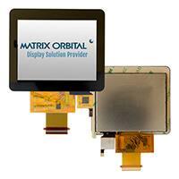
Figure 1: MOP-TFT320240-35G-BLM-TPC Drawing
5
MOP-TFT320240-35G-BLM-TPC
�7 Electro-Optical Characteristics
Item
Response time
Contrast ratio
Surface
luminance
Luminance
uniformity
NTSC
Symbol
Tr + Tf
Cr
Viewing angle
T
CIE (x, y)
chromaticity
Red x
Red y
Green x
Green y
Blue x
Blue y
White x
White y
Condition
-
Min
200
Typ
50
300
Max
80
-
Unit
ms
---
Remark
FIG 1.
FIG 2.
Note
Note 4
Note 1
Lv
θ=0q
350
495
-
cd/m²
FIG 2.
Note 2
Yu
θ=0q
75
80
-
%
FIG 2.
Note 3
50
40
50
50
0.5706
0.3254
0.3000
0.5649
0.1074
0.0387
0.2632
0.2829
60
60
50
60
60
0.6106
0.3654
0.3400
0.6049
0.1474
0.0787
0.3032
0.3229
0.6506
0.4054
0.3800
0.6449
0.1874
0.1187
0.3432
0.3629
%
deg
deg
deg
deg
-
FIG 2.
FIG 3.
FIG 3.
FIG 3.
FIG 3.
Note 5
-
θ=0q
= 90q
= 270q
= 0q
= 180q
θ=0q
=0q
Ta=25°C
FIG 2.
CIE1931
Note 6
Note 5
*Note 1: Definition of contrast ratio
Contrast Ratio (CR) is defined mathematically by the following formula.
�������������� ൌ �
�
���������̶White" �
�
���������̶�
̶ �
*Note 2: Definition of surface luminance
Surface luminance is the LCD luminance from the surface with all pixels displaying white.
� ൌ ���
��
�����ሺ�ͳǡ �ʹǡ �͵ ǥ �ሻ
*Note 3: Definition of luminance uniformity
The luminance uniformity in surface luminance (Yu) is determined by measuring luminance at each test position 1 through n,
and then dividing the maximum luminance of n point’s luminance by minimum luminance of n points luminance.
� ൌ �
���
��
�����ሺ�ͳǡ �ʹǡ �͵ ǥ �
���
��
�����ሺ�ͳǡ �ʹǡ �͵ ǥ �ሻ
*Note 4: Definition of Response time
The response time is defined as the LCD optical switching time interval between “White” state and “Black” state. Rise time
(TON) is the time between photo detector output intensity changed from 90% to 10%. And fall time (TOFF) is the time
between photo detector output intensity changed from 10% to 90%.
*Note 5: Definition of color chromaticity (CIE1931)
CIE (x, y) chromaticity, the x, y value is determined by screen active area center position P5.
*Note 6: Definition of Viewing angle.
Viewing angle is the angle at which the contrast ratio is greater than 10. The angles are determined for the horizontal or x
axis and the vertical or y axis with respect to the z axis which is normal to the LCD surface.
For Viewing angle and response time testing, the testing data is based on Autronic-Melchers’s ConoScope or DMS series
Instruments or compatible. For contrast ratio, Surface Luminance, Luminance uniformity and CIE, the testing data is based on
TOPCON’s BM-7 or BM-5 photo detector or compatible.
*Note 7: For TFT module, Gray scale reverse occurs in the direction of panel viewing angle.
MOP-TFT320240-35G-BLM-TPC
6
�Up
Φ=90
(12:00)
\
θ=0
]
θ
Φ
Left
Φ=180
(9:00)
Right
x Φ=0
(3:00)
Down
Φ=270
(6:00)
Figure 2: The definition of viewing angle
8 Interface Description
8.1 LCM Interface Description
Interface No.
1
2
3
4
5-12
13-20
21-28
29
30
31
32
33
34
35
36
37
38
39
40
Name
LEDK
LEDA
CS
VDD
Red(0-7)
Green(0-7)
Blue(0-7)
GND
DCLK
DISP
HSYNC
VSYNC
DE
SCL
SDA
XR(NC)
YD(NC)
XL(NC)
YU(NC)
I/O Pin Connections
P
P
I
P
I
I
I
I
I
I
I
I
I
I
I/O
-
Description
Power for LED backlight(Cathode)
Power for LED backlight(Anode)
Chip select pin
Power for LCD
Red data
Green data
Blue data
Ground
Dot-clock signal
Display on/off
Horizontal sync input.
Vertical sync input
Data enable
Clock pin of serial interface
Data input pin in serial mode
No connection
No connection
No connection
No connection
8.2 CTP Interface Description
Interface No.
1
2
3
4
5
6
7
Name
RESET
VDD
GND
INT
SCL
SDA
I/O Pin Connection
I
P
P
O
I
I/O
Description
Reset low
Power Supply of CTP
Ground
State change interrupt
Serial interface clock
Serial interface data
MOP-TFT320240-35G-BLM-TPC
�9 AC Characteristics
9.1 Pixel Timing
Figure 3:Pixel Timing
Characteristics
Symbol
DOTCLK Frequency
DOTCLK Period
Vertical Sync Setup Time
Vertical Sync Hold Time
Horizontal Sync Setup Time
Horizontal Sync Hold Time
Phase Difference of Sync
Signal Falling Edge
DOTCLK Low Period
DOTCLK High Period
Data Setup Time
Data Hold Time
Reset pulse width
fDOTCLK
tDOTCLK
tvsys
tvsyh
thsys
thsyh
Min.
24 bit
100
20
20
20
20
thv
tCKL
tCKH
tds
tdh
tRES
Typ.
8 bit
33.3
10
10
10
10
24 bit
6.5
154
-
1
50
50
12
12
Max.
8 bit
19.5
51.3
-
24 bit
10
-
15
15
10
10
-
10
240
-
-
8 bit
30
-
-
MHz
ns
ns
ns
ns
ns
tDOTCLK
-
Unit
ns
ns
ns
ns
μS
*Note: External clock source must be provided to DOTCLK pin of HX8238-D. The driver will not operate if absent of the
clocking signal.
MOP-TFT320240-35G-BLM-TPC
8
�9.2 Data Timing
Figure 4: Data Transaction Timing in Parallel RGB (24Bit) interface (SYNC Mode)
9
Characteristics
Symbol
DOTCLK Frequency
DOTCLK Period
Horizontal Frequency (Line)
Vertical Frequency (Refresh)
Horizontal Back porch
Horizontal Front porch
Horizontal Data Start Point
Horizontal Blanking Period
Horizontal Display Area
Horizontal Cycle
Vertical Back Porch
Vertical Front Porch
Vertical Data Start Point
Vertical Blanking Period
NTSC
Vertical Display
PAL
Area
PAL
Vertical Cycle
NTSC
PAL
fDOTCLK
tDOTCLK
fH
fV
tHBP
tHFP
tHBP
tHBP + tHFP
HDISP
Hcycle
tVBP
tVFP
tVBP
tVBP + tVFP
Min.
24 bit 8 bit
100
33.3
-
VDISP
-
Vcycle
-
Typ.
24 bit
8 bit
6.5
19.5
154
51.3
14.9
60
68
204
20
60
68
204
88
264
320
960
408
1224
18
4
18
22
240
280(PALM=0)
288(PALM=1)
262
313
MOP-TFT320240-35G-BLM-TPC
Max.
24 bit
8 bit
10
30
22.35
90
450
1350
-
MHz
ns
KHz
Hz
tDOTCLK
tDOTCLK
tDOTCLK
tDOTCLK
tDOTCLK
tDOTCLK
Lines
Lines
Lines
Lines
-
Lines
350
Lines
Unit
�10 Power Sequence
10.1 Power Up Sequence
Figure 5: Power Up Sequence
Characteristics
Symbol
VDD/VDDIO on to falling edge of SHUT
DOTCLK
Falling edger of SHUT to display start
- 1 line: 408 CLK
- 1 frame: 262 line
- DOTCLK = 6.5MHz
tp-shut
tclk-shut
Min.
1
1
Spec.
Typ.
-
Max.
-
-
-
14
frame
-
166
232.4
ms
Unit
μS
clk
tshut-on
*Note: it is necessary to input DOTCLK before the falling edge of SHUT. Display starts at 10th falling edge of VSYNC after the
falling edge of SHUT
MOP-TFT320240-35G-BLM-TPC
10
�10.2 Power Down Sequence
Figure 6: Power Down Sequence
Characteristics
Symbol
Rising edge of SHUT to display off
- 1 line: 408 CLK
- 1 frame: 262 line
- DOTCLK = 6.5MHz
tshut-off
Min.
2
Spec.
Typ.
-
Max.
-
frame
33.4
-
-
ms
*Note: DOTCLK must be maintained at least 2 frames after the rising edge of SHUT.
Display turns off at the 2nd falling edge of VSYNC after the falling edge of SHUT.
If RESET signal is necessary for power down, provide it after the 2- frames-cycle of the SHUT period.
11
MOP-TFT320240-35G-BLM-TPC
Unit
�11 Inspection Criterion
11.1 Description
This specification is made to be used as the standard acceptance/rejection criteria for the
MOP-TFT320240-35G-BLM-TPC.
11.2 Sample plan
Sampling plan according to GB/T2828.1-2003/ISO 2859-1: 1999 and ANSI/ASQC Z1.4-1993, normal level 2 and
based on:
Major defect: AQL 0.65
Minor defect: AQL 1.5
11.3 Inspection condition
x
Viewing distance for cosmetic inspection is about 30±5cm with bare eyes, and under a 600~1000lux
environment for visual inspection and 0~200lux for function test. All directions for inspecting the sample
should be within 45°against perpendicular line. (Normal temperature 18a28qC and normal humidity
60r15�RH).
x
During testing, the LCD is driven using the voltage level (Within r0.5V of the typical value at 25qC.) that
provides the most optical contrast
11.4 Definition of inspection zone in LCD
A
B C
Figure 7: Inspection Zones in an LCD
Zone A: character/Digit area
Zone B: viewing area except Zone A (Zone A + Zone B=minimum Viewing area)
Zone C: Outside viewing area (invisible area after assembly in customer’s product)
*Note: As a general rule, visual defects in Zone C are permissible, if it does not affect display quality and assembly of
customer’s product.
11.5 Function Defect
Items to be inspected
Inspection criterion
All functional defects
Missing
1) No display
2) Display abnormally
3) Missing vertical, horizontal segment
4) Short circuit
5) Back-light no lighting, flickering and abnormal lighting.
6) obvious striation
7) Current beyond specification value
Missing component
Outline dimension
Overall outline dimension exceed the drawing is not allowed.
MOP-TFT320240-35G-BLM-TPC
Classification of defects
MA
12
�11.6 LCD pixel defect
(bad dot) (defect type: MI)
Checking item
Color bad dot-bright dot(R,G,B)
Two adjacent bright point
Three or more adjacent point
Total points for bad dot-bright dot
Bad dot-dark dot
Two adjacent dark point
Three or more adjacent point
Total points for bad dot -dark dot
Patch bright dot
Judgment criterion
1
0
0
1
2
1
0
3
Invisible with ND5%, it is OK.
11.7 Dot and line defect
(defect type: MI)
Checking item
Dot defect
Line defect
Concave point and air
bubble for polarizer
Fold mark, linear scar for
polarizer
13
Judgment criterion
Diameter(mm)\LCD Size
S ≤5.0 Inch
D≤0.1
allowed
0.1
MOP-TFT320240-35G-BLM-TPC 价格&库存
很抱歉,暂时无法提供与“MOP-TFT320240-35G-BLM-TPC”相匹配的价格&库存,您可以联系我们找货
免费人工找货