STDP2600
Advanced HDMI to DisplayPort
converter
Datasheet
Rev A
MegaChips’ Proprietary Information
MegaChips reserves the right to make any change herein at any time without prior notice. MegaChips
does not assume any responsibility or liability arising out of application or use of any product or
service described herein except as explicitly agreed upon.
MegaChips’ Proprietary Information
Page 1 of 33
�STDP2600
Features
•
Spread spectrum on DisplayPort interface for
EMI reduction
•
•
Deep color support
– RGB/YCC (4:4:4) – 16-bit color
– YCC (4:2:2) – 16-bit color
– Color space conversion – YUV to RGB and
RGB to YUV
•
Bandwidth
– Video resolution up to 4K x 2K @ 30 Hz;
1920 x 1080 @ 120 Hz
– Audio 7.1 Ch up to 192 kHz sample rate
•
Low power operation; active 450 mW, standby
21 mW
•
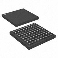
Package
– 81 BGA (8 x 8 mm)
•
Power supply voltages
– 3.3 V I/O; 1.2 V core
•
DisplayPort® (dual mode) transmitter
– DP 1.2a compliant
– Link rate HBR2/HBR/RBR
– 1, 2, or 4 lanes
– AUX CH 1 Mbps
– Supports eDP operation
– HDMI / DVI operation with level translator
HDMI 1.4 receiver
– Link rate up to 2.97 Gbps/data pair
– Color depth up to 48 bits
– 3D video timings
– CEC
•
SPDIF audio output
•
HDCP repeater with embedded keys
•
ASSR–eDP display authentication option
•
I2C to AUX bridge for EDID/MCCS pass
through
•
Device configuration options
– SPI Flash
– I2C host interface
•
Image
Capture
HDMI
Input
Applications
Audio-video accessory (dongle) for
PC/notebooks and docking stations
Video Format
Converter
DP Dual Mode
Transmitter
HDMI
Receiver
SPDIF
Audio
SPDIF
Transmitter
DDC
Controller
CEC
CEC
I2C Slave
C2600-DAT-01p
DP++
Output
Clock
Generation
OCM, SPI
MegaChips’ Proprietary Information
Page 2 of 33
I2C to AUX
Bridge
DDC
AUX
�STDP2600
Contents
1.
Description . . . . . . . . . . . . . . . . . . . . . . . . . . . . . . . . . . . . . . . . . . . . . . . . . 7
2.
Application overview . . . . . . . . . . . . . . . . . . . . . . . . . . . . . . . . . . . . . . . . . . 8
3.
Feature attributes . . . . . . . . . . . . . . . . . . . . . . . . . . . . . . . . . . . . . . . . . . . . 9
4.
5.
6.
7.
3.1
Input interface . . . . . . . . . . . . . . . . . . . . . . . . . . . . . . . . . . . . . . . . . . . . . . 9
3.2
Output interface . . . . . . . . . . . . . . . . . . . . . . . . . . . . . . . . . . . . . . . . . . . . . 9
3.3
Deep color support . . . . . . . . . . . . . . . . . . . . . . . . . . . . . . . . . . . . . . . . . . 10
3.4
Supported video timings . . . . . . . . . . . . . . . . . . . . . . . . . . . . . . . . . . . . . . 10
3.5
Supported audio timings . . . . . . . . . . . . . . . . . . . . . . . . . . . . . . . . . . . . . . 10
3.6
Control channel interfaces . . . . . . . . . . . . . . . . . . . . . . . . . . . . . . . . . . . . 10
3.7
HDCP 1.3 support . . . . . . . . . . . . . . . . . . . . . . . . . . . . . . . . . . . . . . . . . . 10
3.8
Package . . . . . . . . . . . . . . . . . . . . . . . . . . . . . . . . . . . . . . . . . . . . . . . . . . .11
3.9
Power supply voltages . . . . . . . . . . . . . . . . . . . . . . . . . . . . . . . . . . . . . . . .11
3.10
ESD . . . . . . . . . . . . . . . . . . . . . . . . . . . . . . . . . . . . . . . . . . . . . . . . . . . . . .11
BGA footprint and pin lists . . . . . . . . . . . . . . . . . . . . . . . . . . . . . . . . . . . . . 12
4.1
Ball grid array diagram . . . . . . . . . . . . . . . . . . . . . . . . . . . . . . . . . . . . . . . 12
4.2
Full pin list sorted by pin number . . . . . . . . . . . . . . . . . . . . . . . . . . . . . . . 14
Connections . . . . . . . . . . . . . . . . . . . . . . . . . . . . . . . . . . . . . . . . . . . . . . . 16
5.1
Pin list . . . . . . . . . . . . . . . . . . . . . . . . . . . . . . . . . . . . . . . . . . . . . . . . . . . . 16
5.2
Bootstrap configuration . . . . . . . . . . . . . . . . . . . . . . . . . . . . . . . . . . . . . . 19
Package specifications . . . . . . . . . . . . . . . . . . . . . . . . . . . . . . . . . . . . . . . 20
6.1
Package drawing . . . . . . . . . . . . . . . . . . . . . . . . . . . . . . . . . . . . . . . . . . . 20
6.2
BGA8X8 dimensions . . . . . . . . . . . . . . . . . . . . . . . . . . . . . . . . . . . . . . . . 21
6.3
Marking field template and descriptors . . . . . . . . . . . . . . . . . . . . . . . . . . . 22
6.4
Classification reflow profile . . . . . . . . . . . . . . . . . . . . . . . . . . . . . . . . . . . . 22
Electrical specifications . . . . . . . . . . . . . . . . . . . . . . . . . . . . . . . . . . . . . . . 23
7.1
Absolute maximum ratings . . . . . . . . . . . . . . . . . . . . . . . . . . . . . . . . . . . . 23
7.2
DC characteristics . . . . . . . . . . . . . . . . . . . . . . . . . . . . . . . . . . . . . . . . . . 23
C2600-DAT-01p
MegaChips’ Proprietary Information
Page 3 of 33
�STDP2600
7.3
AC characteristics . . . . . . . . . . . . . . . . . . . . . . . . . . . . . . . . . . . . . . . . . . 24
7.3.1
DisplayPort transmitter . . . . . . . . . . . . . . . . . . . . . . . . . . . . . . . . . . . . . 25
7.3.2
HMDI receiver . . . . . . . . . . . . . . . . . . . . . . . . . . . . . . . . . . . . . . . . . . . . 26
7.3.3
HDMI transmitter . . . . . . . . . . . . . . . . . . . . . . . . . . . . . . . . . . . . . . . . . . 27
7.3.4
Crystal specification . . . . . . . . . . . . . . . . . . . . . . . . . . . . . . . . . . . . . . . . 28
7.3.5
I2C interface timing . . . . . . . . . . . . . . . . . . . . . . . . . . . . . . . . . . . . . . . . 28
7.3.6
SPI interface timing . . . . . . . . . . . . . . . . . . . . . . . . . . . . . . . . . . . . . . . . 29
8.
Ordering information . . . . . . . . . . . . . . . . . . . . . . . . . . . . . . . . . . . . . . . . . 31
9.
Revision history . . . . . . . . . . . . . . . . . . . . . . . . . . . . . . . . . . . . . . . . . . . . . 32
C2600-DAT-01p
MegaChips’ Proprietary Information
Page 4 of 33
�STDP2600
List of Tables
Table 1.
Table 2.
Table 3.
Table 4.
Table 5.
Table 6.
Table 7.
Table 8.
Table 9.
Table 10.
Table 11.
Table 12.
Table 13.
Table 14.
Table 15.
Table 16.
Table 17.
Table 18.
Table 19.
Table 20.
Table 21.
Table 22.
Table 23.
Key to BGA diagrams . . . . . . . . . . . . . . . . . . . . . . . . . . . . . . . . . . . . . . . . . . . . . . . . . . . . . 12
Pin list . . . . . . . . . . . . . . . . . . . . . . . . . . . . . . . . . . . . . . . . . . . . . . . . . . . . . . . . . . . . . . . . . 14
HDMI receiver pins . . . . . . . . . . . . . . . . . . . . . . . . . . . . . . . . . . . . . . . . . . . . . . . . . . . . . . . 16
System function pins. . . . . . . . . . . . . . . . . . . . . . . . . . . . . . . . . . . . . . . . . . . . . . . . . . . . . . 16
General purpose input/output and multi-function pins . . . . . . . . . . . . . . . . . . . . . . . . . . . . 17
Transmitter pins . . . . . . . . . . . . . . . . . . . . . . . . . . . . . . . . . . . . . . . . . . . . . . . . . . . . . . . . . 17
System power and ground . . . . . . . . . . . . . . . . . . . . . . . . . . . . . . . . . . . . . . . . . . . . . . . . . 18
Reserved pins . . . . . . . . . . . . . . . . . . . . . . . . . . . . . . . . . . . . . . . . . . . . . . . . . . . . . . . . . . . 18
Bootstrap configuration . . . . . . . . . . . . . . . . . . . . . . . . . . . . . . . . . . . . . . . . . . . . . . . . . . . . 19
Field descriptors . . . . . . . . . . . . . . . . . . . . . . . . . . . . . . . . . . . . . . . . . . . . . . . . . . . . . . . . . 22
Absolute maximum ratings . . . . . . . . . . . . . . . . . . . . . . . . . . . . . . . . . . . . . . . . . . . . . . . . . 23
DC characteristics. . . . . . . . . . . . . . . . . . . . . . . . . . . . . . . . . . . . . . . . . . . . . . . . . . . . . . . . 23
Maximum speed of operation . . . . . . . . . . . . . . . . . . . . . . . . . . . . . . . . . . . . . . . . . . . . . . . 24
DisplayPort transmitter electrical parameters . . . . . . . . . . . . . . . . . . . . . . . . . . . . . . . . . . . 25
HDMI receiver DC characteristics. . . . . . . . . . . . . . . . . . . . . . . . . . . . . . . . . . . . . . . . . . . . 26
HDMI receiver AC characteristics . . . . . . . . . . . . . . . . . . . . . . . . . . . . . . . . . . . . . . . . . . . . 27
HDMI transmitter (DP++) DC characteristics . . . . . . . . . . . . . . . . . . . . . . . . . . . . . . . . . . . 27
HDMI transmitter AC characteristics. . . . . . . . . . . . . . . . . . . . . . . . . . . . . . . . . . . . . . . . . . 27
Crystal specifications . . . . . . . . . . . . . . . . . . . . . . . . . . . . . . . . . . . . . . . . . . . . . . . . . . . . . 28
I2C interface timing . . . . . . . . . . . . . . . . . . . . . . . . . . . . . . . . . . . . . . . . . . . . . . . . . . . . . . . 28
SPI interface timing, VDD = 3.3V . . . . . . . . . . . . . . . . . . . . . . . . . . . . . . . . . . . . . . . . . . . . 29
Order codes . . . . . . . . . . . . . . . . . . . . . . . . . . . . . . . . . . . . . . . . . . . . . . . . . . . . . . . . . . . . 31
Document revision history . . . . . . . . . . . . . . . . . . . . . . . . . . . . . . . . . . . . . . . . . . . . . . . . . 32
C2600-DAT-01p
MegaChips’ Proprietary Information
Page 5 of 33
�STDP2600
List of Figures
Figure 1.
Figure 2.
Figure 3.
Figure 4.
Figure 5.
Figure 6.
Figure 7.
Figure 8.
Figure 9.
STDP2600 in BD player/game console accessory application . . . . . . . . . . . . . . . . . . . . . . . 8
STDP2600 BGA diagram . . . . . . . . . . . . . . . . . . . . . . . . . . . . . . . . . . . . . . . . . . . . . . . . . . 13
Package drawing . . . . . . . . . . . . . . . . . . . . . . . . . . . . . . . . . . . . . . . . . . . . . . . . . . . . . . . . 20
Package dimensions. . . . . . . . . . . . . . . . . . . . . . . . . . . . . . . . . . . . . . . . . . . . . . . . . . . . . . 21
Marking template . . . . . . . . . . . . . . . . . . . . . . . . . . . . . . . . . . . . . . . . . . . . . . . . . . . . . . . . 22
HDMI and DVI receiver AC characteristics . . . . . . . . . . . . . . . . . . . . . . . . . . . . . . . . . . . . . 27
I2C Timing . . . . . . . . . . . . . . . . . . . . . . . . . . . . . . . . . . . . . . . . . . . . . . . . . . . . . . . . . . . . . 29
SPI output or serial interface SPI ROM input timing . . . . . . . . . . . . . . . . . . . . . . . . . . . . . . 30
SPI input or serial interface SPI ROM output timing . . . . . . . . . . . . . . . . . . . . . . . . . . . . . . 30
C2600-DAT-01p
MegaChips’ Proprietary Information
Page 6 of 33
�STDP2600
1.
Description
The STDP2600 is a high-speed HDMI to DisplayPort converter IC targeted for applications such as
audio-video accessories, docking stations, notebook motherboard designs, etc. This device includes an
HDMI 1.4 compliant receiver and a VESA DP Standard Ver. 1.2a compliant dual mode transmitter,
implementing a single link DisplayPort output port comprising four Main lanes, AUX CH, and HPD.
The STDP2600 uses MegaChips’ latest generation DisplayPort dual mode transmitter technology that
supports both DisplayPort and TMDS signal formats (DP++). DisplayPort transmitter supports HBR2
speed, a data rate of 5.4 Gbps per lane with a total bandwidth of 21.6 Gbps link rate. The transmitter is
also capable of supporting HDMI or single link DVI output through a passive level translator (dongle). The
HDMI receiver unit supports link rate up to 2.97 Gbps that corresponds to a pixel rate of 297 MHz,
adequate for handling video timings up to FHD 120 Hz 3D formats. This device delivers deep color video
up to 16-bits per color at 1080p 60 Hz and lower video resolutions. STDP2600 allows audio transport
from the source to desired audio rendering devices over the DP++ output or through the SPDIF port. The
audio signal from the source can be routed simultaneously to DP++ and SPDIF output ports. For
example, STDP2600 allows routing of any two audio channels on the SPDIF port, while transporting up
to eight channels on the DP++ port.
The STDP2600 supports RGB and YCbCr colorimetric formats with color depth of 16, 12, 10, and 8 bits.
This device features HDCP 1.3 content protection scheme with an embedded key option for secure
transmission of digital audio-video content. It also operates as an HDCP repeater for the downstream
sink. The eDP authentication option ASSR (Alternative Scrambler Seed Reset) is supported for
embedded application.
The I2C-to-AUX translator in STDP2600 allows the upstream HDMI source to access EDID and transfer
MCCS commands to a downstream DisplayPort sink device over the DisplayPort interface. This device
has an on-chip microcontroller with SPI and I2C host interface for system configuration purposes.
STDP2600 can be configured with an external SPI Flash for custom applications. In addition, it allows
register level configuration from an external host controller through I2C interface.
C2600-DAT-01p
MegaChips’ Proprietary Information
Page 7 of 33
�STDP2600
2.
Application overview
Figure 1. STDP2600 in BD player/game console accessory application
HDMI signal
27 MHz
Crystal
STDP2600
DP Main Lanes
AUX CH
CEC
DDC
C2600-DAT-01p
MegaChips’ Proprietary Information
Page 8 of 33
DP++
HDMI
SPI
Flash
�STDP2600
3.
Feature attributes
3.1
Input interface
• HDMI standard Ver. 1.4 compliant (DC coupled)
• Link rate: 2.97 Gbps/data pair max
• Video: HDMI 1.4 primary and secondary timing formats, as well as CEA861 timing formats with
pixel repetition for lower resolutions
• Deep color encoding up to 48 bits/pixel in 444 and 422; encoding in 601, 709, and IEC61966
color spaces
• Audio: IEC60958 L-PCM and IEC61937 streams up to 24 bits/sample from 32 kHz to 192 kHz
• DDC slave port
• HPD assertion
3.2
Output interface
• DP++ interface featuring
– AC coupled DisplayPort Ver. 1.2a compliant transmitter; supports eDP
– AC coupled HDMI 1.4 transmitter (with external level shifter)
• DP main link configuration (SST format only, no MST format support)
– HBR2/HBR/RBR link rate
– 1, 2, or 4 lanes
• AUX CH: Manchester transaction format
• HPD: IRQ_HPD assertion
• Video: EDID 1.4 and CEA861 video timing and formats from 24 to 48 bits/pixel in RGB or
YCC422 or YcC444 colorimetry
• Audio: DisplayPort 1.2a standard info frame packets and IEC60958/61937 type audio stream
packets ranging from 16 to 24 bits/sample, 32 to 192 kHz sample rates
• HDMI link rate: 2.97 Gbps/data pair max
C2600-DAT-01p
MegaChips’ Proprietary Information
Page 9 of 33
�STDP2600
3.3
Deep color support
• RGB/YCC (4:4:4) – 16-bit color
• YCC (4:2:2) – 16-bit color
• Color space conversion – YUV to RGB and RGB to YUV
3.4
Supported video timings
• 4096 x 2160 (4K x 2K) 24 Hz/30 Hz; 24 bits/pixel
• 1920 x 1080 (FHD) 120 Hz: 24 bits/pixel
• 2560 x 1600 (WQXGA) 60 Hz: 24 bits/pixel
• Up to 1920 x 1080 (FHD) 60 Hz, 48, 36, 30 bits/pixel
• All compatible 3D formats defined in DP 1.2a and HDMI 1.4 specifications
• All standard CEA861 timing formats
3.5
Supported audio timings
• All audio formats as specified in DP 1.2a and HDMI 1.4 specifications
• SPDIF; 2-Ch LPCM, AC3, DTS, bit depth up to 24 bits, sample rate up to 192 kHz
3.6
Control channel interfaces
• AUX CH, I2C host interface, SPI (optional), and UART (UART for test/debug purposes only)
3.7
HDCP 1.3 support
• Key sets for HDMI RX and DP/HDMI TX integrated in one-time programmable ROM (OTP)
• Standalone HDCP repeater capability
• Supports eDP display authentication option ASSR (Alternate Scrambler Seed Reset)
C2600-DAT-01p
MegaChips’ Proprietary Information
Page 10 of 33
�STDP2600
3.8
Package
• 81 BGA (8 x 8 mm), 0.8 ball pitch
3.9
Power supply voltages
• 3.3 V I/O; 1.2 V core
3.10 ESD
• 2 KV HBM, 500 V CDM
C2600-DAT-01p
MegaChips’ Proprietary Information
Page 11 of 33
�STDP2600
4.
BGA footprint and pin lists
4.1
Ball grid array diagram
The ball grid array (BGA) diagrams give the allocation of pins to the package, shown from the top looking
down using the PCB footprint.
Some signal names in BGA diagrams have been abbreviated. Refer toTable 2: Pin list on page 14 for full
signal names sorted by pin number.
Table 1. Key to BGA diagrams
C2600-DAT-01p
Function
Type
AVDD12_RX
VCC/VDD
AVDD33_RX
VCC/VDD
AVDD33_RCOSC
VCC/VDD
AVDD12_TX
VCC/VDD
AVDD33_TX
VCC/VDD
DVDD12
VCC/VDD
DVDD33
VCC/VDD
System ground
VSS/GND
No connect/Do not connect
NC/DNC
MegaChips’ Proprietary Information
Page 12 of 33
Key
�STDP2600
The STDP2600 is available in an 81-pin BGA package.
Figure 2. STDP2600 BGA diagram
01
02
03
04
05
06
07
08
09
A
HDMI_RX2P
HDMI_RX2N
HDMI_RX1P
HDMI_RX1N
HDMI_RX0P
HDMI_RX0N
HDMI_RXCKP
HDMI_RXCKN
N/C
A
B
SPI_DI
SPI_CSN
AVDD12_RX
AVDD12_RX
AVDD33_RX
CPHY_RX_REXT
AVDD12_PLL
TEST_MISN
N/C
B
C
SPI_CLK
SPI_DO
VSS
VSS
AVDD33_RX
AVDD33_RX
AVDD33_RCOSC
TESTMODE0_
CONFIG1
UART_RX
C
D
PWR_CTRL
I2C_SDA
DVDD12
VSS
VSS
VSS
DVDD12
TESTMODE1_
CONFIG2
UART_TX
D
E
CHRG_CTRL
I2C_SCL
DVDD12
VSS
VSS
VSS
DVDD12
VSS
IRQ
E
F
PWR_SENSE
SPDIF
DVDD33
VSS
VSS
VSS
VSS
HPD_OUT_
AUX_HPD
CEC
F
G
HPD_IN
HDMI_DDC_SDA
DVDD33
VSS
VSS
AVDD33_TX
VSS
RESETn
XTAL
G
H
DPTX_AUXN
HDMI_DDC_SCL
TX_REXT
AVDD12_TX
AVDD12_TX
AVDD12_TX
AVDD12_OSC
DVDD25_SM
TCLK
H
J
DPTX_AUXP
DPTX_L3N_
HDMI_TXCKN
DPTX_L3P_
HDMI_TXCKP
DPTX_L2N_
HDMI_TX0N
DPTX_L2P_
HDMI_TX0P
DPTX_L1N_
HDMI_TX1N
DPTX_L1P_
HDMI_TX1P
DPTX_L0N_
HDMI_TX2N
DPTX_L0P_
HDMI_TX2P
J
01
02
03
04
05
06
07
08
09
C2600-DAT-01p
MegaChips’ Proprietary Information
Page 13 of 33
�STDP2600
4.2
Full pin list sorted by pin number
Table 2. Pin list
Pin number
A1
HDMI_RX2P
A2
HDMI_RX2N
A3
HDMI_RX1P
A4
HDMI_RX1N
A5
HDMI_RX0P
A6
HDMI_RX0N
A7
HDMI_RXCKP
A8
HDMI_RXCKN
A9
DNC
B1
SPI_DI
B2
SPI_CSN
B3, B4
AVDD12_RX
B5
AVDD33_RX
B6
CPHY_RX_REXT
B7
AVDD12_PLL
B8
TEST_MISN
B9
DNC
C1
SPI_CLK
C2
SPI_DO
C3, C4
VSS
C5, C6
AVDD33_RX
C7
AVDD33_RCOSC
C8
CONFIG1
C9
UART_RX
D1
PWR_CTRL
D2
I2C_SDA
D3
DVDD12
D4, D5, D6
C2600-DAT-01p
Net name
VSS
D7
DVDD12
D8
CONFIG2
D9
UART_TX
E1
CHRG_CTRL
E2
I2C_SCL
MegaChips’ Proprietary Information
Page 14 of 33
�STDP2600
Table 2. Pin list (continued)
Pin number
E3
E4, E5, E6
DVDD12
VSS
E7
DVDD12
E8
VSS
E9
IRQ
F1
PWR_SENSE
F2
SPDIF
F3
DVDD33
F4, F5, F6, F7
VSS
F8
HPD_OUT_AUX_HPD
F9
CEC
G1
HPD_IN
G2
HDMI_DDC_SDA
G3
DVDD33
G4, G5
VSS
G6
AVDD33_TX
G7
VSS
G8
RESETn
G9
XTAL
H1
DPTX_AUXN
H2
HDMI_DDC_SCL
H3
TX_REXT
H4, H5, H6
C2600-DAT-01p
Net name
AVDD12_TX
H7
AVDD12_OSC
H8
DVDD25_SM
H9
TCLK
J1
DPTX_AUXP
J2
DPTX_L3N_HDMI_TXCKN
J3
DPTX_L3P_HDMI_TXCKP
J4
DPTX_L2N_HDMI_TX0N
J5
DPTX_L2P_HDMI_TX0P
J6
DPTX_L1N_HDMI_TX1N
J7
DPTX_L1P_HDMI_TX1P
J8
DPTX_L0N_HDMI_TX2N
J9
DPTX_L0P_HDMI_TX2P
MegaChips’ Proprietary Information
Page 15 of 33
�STDP2600
5.
Connections
5.1
Pin list
I/O Legend: I = Input; O = Output; P = Power; G = Ground; IO = Bi-direction; AI = Analog input; AO =
Analog output; AIO = Analog I/O; TRI = Tristate; TOL = Tolerance; PD = Internal 50K pulldown; PU =
Internal 50K pull-up; OPENDR = Open drain output
Note:
Some pins can have multiple functionalities, which are configured under register control.
The alternate functionality for each pin is listed in the Description column.
Table 3. HDMI receiver pins
Pin
Assignment
I/O
Description
Reset state
B6
CPHY_RX_REXT
AI, 3V3 tol
Combo receiver external 249 ohm resistor to VDD33.
NA
A8
HDMI_RXCKN
A7
HDMI_RXCKP
A6
HDMI_RX0N
A5
HDMI_RX0P
AI, 3V3 tol
Direct Connect From HDMI Connector
Input
A4
HDMI_RX1N
A3
HDMI_RX1P
A2
HDMI_RX2N
A1
HDMI_RX2P
Table 4. System function pins
Pin
Assignment
I/O
Description
Reset state
B8
TEST_MISN
I, 3V3 tol,
TRI, INT PD
Connect to GND
Input, Low
H9
TCLK
AIO, 1V2 tol
G9
XTAL
AIO, 1V2 tol
G8
RESETn
AIO, 3V3 tol
3K ohm resistor to 3.3V
NA
B2
SPI_CSN
IO, 3V3 tol,
TRI, INT PU
To SPI chip select. Also see bootstraps.
Output, High
C2
SPI_DO
IO, 3V3 tol,
TRI INT PD
To SPI data out. Also see bootstraps.
Output, Low
B1
SPI_DI
IO, 3V3 tol,
TRI, INT PD
From SPI data in.
Input, Low
C1
SPI_CLK
IO, 3V3 tol,
TRI, INT PD
To SPI clock. Also see bootstraps.
Output, Low
Connect to 27 MHz crystal oscillator with 22 pF to 1.2V NA
C2600-DAT-01p
MegaChips’ Proprietary Information
Page 16 of 33
�STDP2600
Table 5. General purpose input/output and multi-function pins
Pin
Assignment
I/O
Description
Reset state
F9
CEC
3.3V IO, 5V tol,
To HDMI CEC pin. 100K res to 3.3V.
OPENDR
F8
HPD_OUT_AUX_H
PD
IO, 3V3 tol, TRI
To the upstream HPD signal pin on the HDMI
connector. 100K res to GND.
E9
IRQ
IO, 3V3 tol, TRI
GPIO/IRQ out for host interface. Also see bootstrap
TRI, Low
function.
D9
UART_TX
IO, 3V3 tol,
OPENDR
To debug port UART_TX/alt I2C_SDA/GPIO. Needs
OPENDR
external 2K res to 3.3V, FS, FT
C9
UART_RX
IO, 3V3 tol,
OPENDR
To debug port UART_RX/alt I2C_SCL/GPIO. Needs
Input
external 2K res to 3.3V, FS, FT
F2
SPDIF
IO, 3V3 tol,
TRI, PU
To external buffer for SPDIF output or use as GPIO.
Output, High
Also see bootstrap function.
G1
HPD_IN
IO, 5V tol,
OPENDR
From HDMI or DP sink connector. Needs 100K to
GND.
D1
PWR_CTRL
IO, 3V3 tol, TRI Use as GPIO
Output
E1
CHRG_CTRL
IO, 3V3 tol, TRI Use as GPIO
Output
D2
I2C_SDA
IO, 3V3 tol, TRI GPIO/I2C_SDA slave or master, FS, FT
TRI
E2
I2C_SCL
IO, 3V3 tol, TRI GPIO/I2C_SCL slave or master, FS, FT
TRI
F1
PWR_SENSE
IO/AI, 3V3 tol,
OPENDR
GPIO/power sense analog/level sensing input, FS,
FT
OPENDR
G2
HDMI_DDC_SDA
GPIO/HDMI DDC SDA, FS, FT
OPENDR
H2
HDMI_DDC_SCL
IO, 5V tol,
OPENDR
GPIO/HDMI DDC SCL, FS, FT
OPENDR
D8
CONFIG2
OPENDR
Output
Input
Input
IO, 3V3 tol, TRI GPIO, 3.3V PAD
C8
CONFIG1
Input
Table 6. Transmitter pins
Pin
Assignment
I/O
Description
Reset state
H3
TX_REXT
AI, 1V2 tol
Transmitter, external 249 ohm resistor to VDD12
NA
H1
DPTX_AUXN
AIO, 1V2 tol
Dual mode transmitter DPTX_AUXN. AC couple to
TX connector. External 100 K resistor to GND.
Tristate
J1
DPTX_AUXP
AIO, 1V2 tol
Dual mode transmitter DPTX_AUXP. AC couple to
TX connector. External 100 K resistor to VDD33.
Tristate
J2
DPTX_L3N_HDMI_
AIO, 1V2 tol
TXCKN
Dual mode transmitter HDMI_TXCKN or
DPTX_L3N. AC couple to TX connector.
Output
J3
DPTX_L3P_HDMI_
TXCKP
Dual mode transmitter HDMI_TXCKP or DPTX_L3P.
Output
AC couple to TX connector.
J4
DPTX_L2N_HDMI_
AIO, 1V2 tol
TX0N
Dual mode transmitter HDMI_TX0N or DPTX_L2N.
AC couple to TX connector.
Output
J5
DPTX_L2P_HDMI_
TX0P
Dual mode transmitter HDMI_TX0P or DPTX_L2P.
AC couple to TX connector.
Output
C2600-DAT-01p
AIO, 1V2 tol
AIO, 1V2 tol
MegaChips’ Proprietary Information
Page 17 of 33
�STDP2600
Table 6. Transmitter pins
Pin
Assignment
J6
Description
Reset state
DPTX_L1N_HDMI_
AIO, 1V2 tol
TX1N
Dual mode transmitter HDMI_TX1N or DPTX_L1N.
AC couple to TX connector.
Output
J7
DPTX_L1P_HDMI_
TX1P
AIO, 1V2 tol
Dual mode transmitter HDMI_TX1P or DPTX_L1P.
AC couple to TX connector.
Output
J8
DPTX_L0N_HDMI_
AIO, 1V2 tol
TX2N
Dual mode transmitter HDMI_TX2N or DPTX_L0N.
AC couple to TX connector.
Output
J9
DPTX_L0P_HDMI_
TX2P
Dual mode transmitter HDMI_TX2P or DPTX_L0P.
AC couple to TX connector.
Output
Note:
I/O
AIO, 1V2 tol
The default DP and HDMI output signals mapping match the standard DP and HDMI
connector pin mapping. However lane swapping and polarity swapping is possible through
software configuration.
Table 7. System power and ground
Pin
Assignment
Description
F3, G3
DVDD33
I/O VDD, 3.3V digital supply. De-couple using 100 nF.
D3, D7, E3, E7
DVDD12
Core VDD, 1.2V digital supply. De-couple using 100 nF.
C7
AVDD33_RCOSC
3.3V RC-oscillator analog supply. De-couple using 100 nF.
B7
AVDD12_PLL
1.2V analog PLL supply. De-couple using 10 uF and 100 nF.
B3, B4
AVDD12_RX
1.2V analog receiver supply. EMI filter rail and de-couple using 10 uF
and 100 nF.
B5, C5, C6
AVDD33_RX
3.3V analog receiver supply. EMI filter rail and de-couple using 10 uF
and 100 nF.
G6
AVDD33_TX
3.3V analog transmitter supply. EMI filter rail and de-couple using 10
uF and 100 nF.
H4, H5, H6
AVDD12_TX
1.2V analog transmitter supply. EMI filter rail and de-couple using 10
uF and 100 nF.
H7
AVDD12_OSC
1.2V analog crystal oscillator supply. De-couple using 100 nF.
H8
DVDD25_SM
Decoupling point for internal 2.5V LDO supply. De-couple using 10 uF
and 100 nF.
C3, C4, D4, D5,
D6, E4, E5, E6, E8,
VSS
F4, F5, F6, F7, G4,
G5, G7
Common GND. Connect to GND plane
Table 8. Reserved pins
Pin
Assignment
A9
DNC
B9
DNC
Description
Reserved. Do not connect
C2600-DAT-01p
MegaChips’ Proprietary Information
Page 18 of 33
�STDP2600
5.2
Bootstrap configuration
DC Levels on some device pins are specified during de-asserting edge of power-on reset (RESETn goes
High). The levels specified below must be adhered to for normal function of the device.
Table 9. Bootstrap configuration
BS signal name
Internal
Assignment Function
PU/PD
IROM_DEBUGn_Bootstrap5
PULL
UP
SPI_CSN
Reserved. SPI_CSN must not be Pulled Down during
Power-On RESET.
XTAL_OSC_SEL_Bootstrap4
PULL
UP
SPDIF_OUT
Reserved. SPDIF_OUT must not be Pulled Down during
Power-On RESETn.
ICD_DEBUG_Bootstrap3
PULL
DN
SPI_DO
Reserved. SPI_DO must not be Pulled Up during Power-On
RESETn.
XROM_EN_Bootstrap2
PULL
DN
SPI_CLK
Reserved. SPI_CLK must not be Pulled Up during PowerOn RESETn.
RESERVED_Bootstrap1
PULL
DN
IRQ
Reserved. IRQ pin must not be Pulled Up during Power-On
RESETn.
ATE_MODE_EN_Bootstrap0
Open
drain
UART_TX
Reserved. UART_TX must be Pulled Up during Power-On
RESETn.
Note:
When the pin corresponding to a specific bootstrap is left NC, it will take the value of the
assigned by the internal PULLUP (Level 1) or PULLDN (Level0). The internal resistor used
is around 50k ohm. To select a non-default value on a bootstrap, an external PULLUP or
PULLDN resistor tied to the opposite direction that overcomes the internal PULLUP or
PULLDN needs to be used.
C2600-DAT-01p
MegaChips’ Proprietary Information
Page 19 of 33
�STDP2600
6.
Package specifications
Package type: 81 BGA (8 x 8 mm / ball pitch 0.8 mm)
6.1
Package drawing
Figure 3. Package drawing
C2600-DAT-01p
MegaChips’ Proprietary Information
Page 20 of 33
�STDP2600
6.2
BGA8X8 dimensions
Figure 4. Package dimensions
Note:
(1) – LFBGA stands for Low profile Fine pitch Ball Grid Array.
– Low profile: 1.20mm < A = 1.70mm / Fine pitch: e < 1.00mm.
– The total profile height (Dim A) is measured from the seating plane “C” to the top of the
component.
– The maximum total package height is calculated by the RSS method (Root Sum Square):
A Max = A1 Typ + A2 Typ + A4 Typ + v (A1² + A2² + A4² tolerance values).
(2) – The typical ball diameter before mounting is 0.50mm.
(3) – The tolerance of position that controls the location of the pattern of balls with respect to
datums A and B. For each ball there is a cylindrical tolerance zone eee perpendicular to
datum C and located on true position with respect to datums A and B as defined by e. The
axis perpendicular to datum C of each ball must lie within this tolerance zone.
4) – The tolerance of position that controls the location of the balls within the matrix with
respect to each other. For each ball there is a cylindrical tolerance zone fff perpendicular to
datum C and located on true position as defined by e. The axis perpendicular to datum C of
each ball must lie within this tolerance zone. Each tolerance zone fff in the array is
contained entirely in the respective zone eee above The axis of each ball must lie
simultaneously in both tolerance zones.
(5) – The terminal A1 corner must be identified on the top surface by using a corner
chamfer, ink or metalized markings, or other feature of package body or integral heat slug.
– A distinguishing feature is allowable on the bottom surface of the package to identify the
terminal A1 corner. Exact shape of each corner is optional.
C2600-DAT-01p
MegaChips’ Proprietary Information
Page 21 of 33
�STDP2600
6.3
Marking field template and descriptors
The STDP2600 marking template is shown below.
Figure 5. Marking template
Field descriptors are shown below.
Table 10.Field descriptors
Field
Description
Marking
A
Product code
STDP2600
B
2-character assembly plant code
99
C
3-character BE sequence code
“XYZ”
D
2-character diffusion plant code
VQ
E
3-character country of origin code
MYS
F
1-digit assembly year
“Y”
G
2-digit assembly week
“WW”
H
Standard MegaChips logo
M
I
2-character version code
AD
J
Ball A1 identifier
a DOT
6.4
Classification reflow profile
Please refer to the DisplayPort Application Note: Classification reflow profile for SMD
devices (C0353-APN-06) for reflow diagram and details.
C2600-DAT-01p
MegaChips’ Proprietary Information
Page 22 of 33
�STDP2600
7.
Electrical specifications
7.1
Absolute maximum ratings
Applied conditions greater than those listed under “Absolute maximum ratings” may cause permanent
damage to the device. The device should never exceed absolute maximum conditions since it may affect
device reliability.
Table 11. Absolute maximum ratings
Parameter
Symbol
Min
Typ
Max
Units
VVDD_3.3
-0.3
3.3
3.63
V
VVDD_1.2
-0.3
1.2
1.26
V
Input voltage for tolerance for 5V I/O pin
VIN5Vtol
-0.3
5.5
V
Input voltage tolerance for 3.3V I/O pin(1,2)
VIN3V3tol
-0.3
3.63
V
ESD - Human Body Model (HBM)
VESD
±2
kV
ESD - Charged Device Model (CDM)
VESD
±500
V
Latch-up
ILA
±200
mA
Ambient operating temperature
TA
0
70
°C
Storage temperature
TSTG
-40
125
°C
Operating junction temperature
TJ
0
125
°C
Thermal resistance (Junction to Ambient)
θJA
52.4
°C/W
Thermal resistance (Junction to Case)
θJC
24.4
°C/W
Peak IR reflow soldering temperature
TSOL
3.3 V supply voltages (1,2)
1.2 V supply voltages
(1.2)
(1,2)
70
260
°C
Note (1): All voltages are measured with respect to GND.
Note (2): Absolute maximum voltage ranges are for transient voltage excursions.
7.2
DC characteristics
Table 12. DC characteristics
Symbol
Min
Typ
Max(1)
Units
3.3 V supply voltages (analog and digital)
VVDD_3.3
3.14
3.3
3.47
V
1.2 V supply voltages (analog and digital)
VVDD_1.2
1.14
1.2
1.26
V
Parameter
Power
Power
Measurement conditions: 1920 x 1080 / 120 Hz
test pattern: ON-OFF dot.
450
Sleep mode
21
C2600-DAT-01p
MegaChips’ Proprietary Information
Page 23 of 33
mW
�STDP2600
Table 12. DC characteristics
Parameter
Symbol
Min
Typ
Max(1)
Units
Supply current
Measurement conditions: 1920 x 1080 / 120 Hz test
pattern: ON-OFF dot Moire
VDD (analog and digital power) = 3.3 V
VDDA (analog and digital power) = 1.2 V
In all configuration, 8 bits input is used.
51
231
mA
Inputs
High voltage
VIH
Low voltage
VIL
Input hysteresis voltage
VHYST
High current (VIN = 3.3V)
IIH
-/+10
μA
Low current (VIN = 0 V)
IIL
-/+10
μA
Capacitance (VIN = 2.4 V)
CIN
5
pF
2.0
V
0.8
300
V
mV
Outputs
High voltage (IOH = 8mA)
VOH
Low voltage (IOL = -8 mA)
VOL
0.4
V
Tri-state leakage current
IOZ
-/+10
μA
Note:
7.3
2.4
V
The values in the Max column represent absolute maximum current consumption under
high voltage (+5%) and nominal temperature. These values are measured in an
environment that includes some discreet components. Other conditions include: a) Power
measurement values are to be used for regulator sizing only, and not directly for package
thermal calculations. b) IC performance is only guaranteed when operating within the “DC
Characteristics”. c) All inputs are 3.3V tolerant.
AC characteristics
Table 13. Maximum speed of operation
Clock domain
Max speed of operation
Reference Input Clock (TCLK)
27 MHz
Reference Internal Clock (RCLK)
324 MHz
On-Chip Microcontroller Clock (OCLK)
100 MHz
SPDIF audio output
192 kHz
2-Wire Serial Slave (SLAVE_SCL)
400 kHz
2-Wire DDC2bi Slave (VGAx_SCL)
400 kHz
2-Wire Serial Master (MSTRx_SCL)
400 kHz
C2600-DAT-01p
MegaChips’ Proprietary Information
Page 24 of 33
�STDP2600
7.3.1 DisplayPort transmitter
Table 14. DisplayPort transmitter electrical parameters
Parameter
Symbol
Min
Typ
Max
Unit
Comments
DisplayPort transmitter system parameters
HBR2 unit interval (5.4
Gbps)
UI_HBR2
Turbo unit interval (3.2
Gbps)
UI_TURBO
312
ps
HBR unit interval (2.7
Gbps)
UI_HBR
370
ps
RBR unit interval (1.62
Gbps)
UI_RBR
617
ps
Link clock down
spreading
Down Spread
Amplitude
185
ps
0
0.5
%
0.8
6.0
dB
Frequency high limit =
+300 ppm
Frequency low limit =
5300 ppm
Modulation frequency
range 0f 30kHz to
33kHz
DisplayPort transmitter TP2 parameters
Ratio of output voltage
level 1/ level 0
Ratio of output voltage
level 2/ level 1
VTX-OUTPUT0.1
5.1
dB
Ratio of output voltage
level 3/ level 2
0.8
6.0
dB
Ratio of output voltage
level 1/ level 0
5.2
6.9
dB
RATION_RBR_HB
R
Ratio of output voltage
level l 2/ level 1
VTX-OUTPUT-
Maximum preemphasis when
disabled
Max output voltage
level
Lane-to-lane output
skew
3.5
dB
1
4.4
dB
0.25
dB
1.2
V
2
UI
Applied to all pairwise
combinations of
supported lanes
4UI+500ps ps
Applied to all pairwise
combinations of
supported lanes
30
Applies to all support
lanes
VTX-PREEMPOFF
VTX-DIFFp-pMAX
LTX-SKEWINTER_PAIR_HBR
_RBR
Lane-to-Lane output
skew
LTX-SKEWINTER_PAIR_HBR
2
Lane intra-pair output
skew
C2600-DAT-01p
Measured on nontransition bits at preemphasis level 0
setting
1.6
RATION_HBR2
Ratio of output voltage
level 3/ level 2
Measured on nontransition bits at preemphasis level 0
setting
LTX-SKEWINTRA_PAIR
MegaChips’ Proprietary Information
Page 25 of 33
dB
�STDP2600
Table 14. DisplayPort transmitter electrical parameters
Parameter
Symbol
Min
Delta of pre-emphasis
Level 1 vs. level 0
Delta of pre-emphasis
level 2 vs. level 1
Typ
2
VTX-PREEMP-
Unit
Comments
dB
1.6
dB
1.6
dB
DELTA
Delta of pre-emphasis
level 3 vs. level 2
Non-transition
reduction output
Voltage level 2
Non-transition
reduction output
Voltage level 1
Max
VTX-
3
dB
3
dB
1.4
dB
0.62
UI
0.49
UI
0.4
UI
0.25
UI
0.23
UI
DIFF_REDUCTIO
N
Non-transition
reduction output
Voltage level 0
Applied to all valid
voltage settings. No
Pre-emphasis Post
Cursor2 applied
VTx_DIFF at each nonzero nominal preemphasis level must
not be lower than the
specific amount less
than VTx_DIFF at the
zero nominal preemphasis level.
Modulation frequency
range 0f 30 kHz to 33
kHz
DisplayPort transmitterTP3_EQ parameters
Maximum TX total jitter
TTXTJ_8b10b_HBR2
Maximum TX
deterministic jitter
Maximum TX total jitter
TTXDJ_8b10b_HBR2
TTX-
For HBR2. Measured
at 1E-9 BER using
HBR2 Compliance
EYE pattern.
TJ_D10.2_HBR2
Maximum TX
deterministic jitter
TTXDJ_D10.2_HBR2
Maximum TX random
jitter
RJ_D10.2_HBR2
TTX-
TX differential peak-to- TTX-DIFFppeak EYE voltage
p_HBR2
110
mV
For HBR2. Measured
at 1E-9 BER using
D10.2 compliance
pattern.
For HBR2. Measured
at 1E-9 BER using
HBR2 Compliance
EYE pattern.
7.3.2 HMDI receiver
Table 15. HDMI receiver DC characteristics
DC characteristics
Min
Input differential voltage level
Input common mode voltage, Vicm1
C2600-DAT-01p
Typ
Max
Units
150
1200
mV
AVcc-400
AVcc-37.5 mV
MegaChips’ Proprietary Information
Page 26 of 33
Notes
�STDP2600
Table 16. HDMI receiver AC characteristics
AC characteristics
Min
Input clock frequency
Differential input (peak-to-peak)
Typ
Max
Units
25
297
MHz
150
1560
mV
Intra-pair skew tolerance
0.4
Tbit
Inter-pair skew tolerance
0.2Tbit +
112ps
Input clock jitter tolerance
0.3
Notes
TMDS clock rates
222.75 MHz and below
TMDS clock rates
above 222.75 MHz
Tbit
Figure 6. HDMI and DVI receiver AC characteristics
TCHAR
TMDSCLK
TBIT
TMDSDATA0
SKEWINTER-PAIR
TMDSDATA1
TMDSDATA2
7.3.3 HDMI transmitter
Table 17. HDMI transmitter (DP++) DC characteristics
DC characteristics
Min
Typ
Single-ended output voltage
400
500
Single-ended high level output voltage,
VH
AVDD
Single-ended low level output voltage,
VL
AVDD-500
Max
Units
Comments
mV
AVDD= 1.2 volt
mV
AVDD= 1.2 volt
Table 18. HDMI transmitter AC characteristics
DC characteristics
Max
Units
Intra-pair skew at source connector,
max
0.15
Tbit
Intra-pair skew at source connector,
max
0.2
Tcharacter
C2600-DAT-01p
Min
Typ
MegaChips’ Proprietary Information
Page 27 of 33
Comments
�STDP2600
Table 18. HDMI transmitter AC characteristics
TMDS differential clock jitter, max
Rise time/fall time
0.25
75
Tbit
ps
7.3.4 Crystal specification
Mode: fundamental
Table 19. Crystal specifications
Parameters
Min
Typ
Max
Units
Nominal frequency
27
MHz
Tolerance
+/- 50
ppm
Load capacitance
22
pF
ESR (effective series resistance)
40
Ohm
Drive level
100
uW
Shunt capacitance
7
Comments
pF
7.3.5 I2C interface timing
Table 20. I2C interface timing
Symbol
Parameter
Conditions
Min
Measured Max
Unit
fSCL
SCL clock rate
Fast mode
0
393
400
kHz
tHD-STA
Hold time START
After this period, the 1st clock
starts
0.6
0.95
-
μs
tLOW
Low period of clock
SCL
1.3
1.1
-
μs
tHIGH
High period of clock
SCL
0.6
0.75
-
μs
Tsu;STA
Setup time for a
repeated START
0.6
1.09
-
μs
tHD;DAT
Data hold time
0
0.96
0.9(1)
μs
tSU;DAT
Data setup time
100
600
-
ns
TBUF
Bus free time between
STOP and START
1.3
1.7 ms
-
μs
Cb
Capacitance load for
each bus line
-
400
pF
tr
Rise time
20
220
300
ns
tf
Fall time
20
25
300
ns
Vnh
Noise margin at high
level
0.2 VDD
0.3
-
V
Vnl
Noise margin at low
level
0.1 VDD
0.28
-
C2600-DAT-01p
For master
MegaChips’ Proprietary Information
Page 28 of 33
�STDP2600
Note:
The maximum tHD;DAT only has to be met if the device does not stretch the low period tLOW
of the SCL signal. In the diagram below, S = start, P = stop, Sr = Repeated start, and SP=
Repeated stop conditions.
Figure 7. I2C Timing
SDA
tf
tLOW
tSU;DAT
tr
tf
tHD;STA
tSP
tr
tBUF
SCL
S
tHD;STA
tHD;DAT
tHIGH
tSU;STA
tSU;STO
Sr
P
S
7.3.6 SPI interface timing
Table 21. SPI interface timing, VDD = 3.3V
Symbol
Parameter
Min
Max
Units
FCLK
Serial clock frequency
-
50
MHz
TSCKH
Serial clock high time
9
-
ns
TSCKL
Serial clock low time
9
-
ns
TSCKR
Serial clock rise time (slew rate)
0.1
-
V/ns
TSCKF
Serial clock fall time (slew rate)
0.1
-
V/ns
TCES
CE# active setup time
5
-
ns
TCEH
CE# active hold time
5
-
ns
TCHS
CE# not active setup time
5
-
ns
TCHH
CE# not active hold time
5
-
ns
TCPH
CE# high time
50
-
ns
TCHZ
CE# high to high-Z output
-
8
ns
TCLZ
SCK low to low-Z output
0
-
ns
TDS
Data in setup time
5
-
ns
TDH
Data in hold time
5
-
ns
TOH
Output hold from SCK change
0
-
ns
TV
Output valid from SCK
-
8
ns
C2600-DAT-01p
MegaChips’ Proprietary Information
Page 29 of 33
�STDP2600
Figure 8. SPI output or serial interface SPI ROM input timing
ROM_CSn (CE#)
ROM_SCLK (SCK)
ROM_SDO (SI )
ROM_SDI (SO)
Figure 9. SPI input or serial interface SPI ROM output timing
ROM_CSn (CE#)
ROM_SCLK (SCK)
ROM_SDI (SO)
ROM_SDO (SI )
C2600-DAT-01p
MegaChips’ Proprietary Information
Page 30 of 33
�STDP2600
8.
Ordering information
Table 22. Order codes
Part number
Description
STDP2600-AD
81 BGA (8 x 8 mm) delivered in trays
STDP2600-ADT
81 BGA (8 x 8 mm) delivered in tape and reel
C2600-DAT-01p
MegaChips’ Proprietary Information
Page 31 of 33
�STDP2600
9.
Revision history
Table 23. Document revision history
Date
Revision
04-Mar-2016
A
C2600-DAT-01p
Changes
Initial release.
MegaChips’ Proprietary Information
Page 32 of 33
�STDP2600
Notice
Semiconductor products may possibly experience breakdown or malfunction. Adequate care should be taken with respect to the safety design
of equipment in order to prevent the occurrence of human injury, fire or social loss in the event of breakdown or malfunction of semiconductor
products
The overview of operations and illustration of applications described in this document indicate the conceptual method of use of the
semiconductor product and do not guarantee operability in equipment in which the product is actually used.
The names of companies and trademarks stated in this document are registered trademarks of the relevant companies.
MegaChips Co. provides no guarantees nor grants any implementation rights with respect to industrial property rights, intellectual property
rights and other such rights belonging to third parties or/and MegaChips Co. in the use of products and of technical information including
information on the overview of operations and the circuit diagrams that are described in this document.
The product described in this document may possibly be considered goods or technology regulated by the Foreign Currency and Foreign
Trade Control Law. In the event such law applies, export license will be required under said law when exporting the product. This regulation
shall be valid in Japan domestic.
In the event the intention is to use the product described in this document in applications that require an extremely high standard of reliability
such as nuclear systems, aerospace equipment or medical equipment for life support, please contact the sales department of MegaChips
Co. in advance.
All information contained in this document is subject to change without notice.
Copyright © 2016 MegaChips Corporation All rights reserved
MegaChips Corporation
Head Quarters
1-1-1 Miyahara, Yodogawa-ku Osaka 532-0003, Japan
TEL: +81-6-6399-2884
MegaChips Corporation
Taiwan Branch
RM. B 2F, Worldwide House, No.129,
Min Sheng E. Rd., Sec. 3, Taipei 105, Taiwan
TEL: +886-2-2547-1297
MegaChips Corporation
Tokyo Office
17-6 Ichiban-cho, Chiyoda-ku, Tokyo 102-0082, Japan
TEL: +81-3-3512-5080
MegaChips Corporation
Tainan Office
RM. 2, 8F, No.24, Da Qiao 2 Rd., Yong Kang Dist.,
Tainan 710, Taiwan
TEL: +886-6-302-2898
MegaChips Corporation
Makuhari Office
1-3 Nakase Mihama-ku Chiba 261-8501, Japan
TEL: +81-43-296-7414
MegaChips Corporation
Zhunan Office
No.118, Chung-Hua Rd., Chu-Nan, Miao-Li 350, Taiwan
TEL: +886-37-666-156
MegaChips Corporation
San Jose Office
2033 Gateway Place, Suite 400, San Jose, CA 95110 U.S.A.
TEL: +1-408-570-0555
MegaChips Corporation
Shenzhen Office
Room 6307, Office Tower, Shun Hing Square, 5002
Shen Nan Dong Road, Luohu District,
Shenzhen 518000, P. R. China
TEL: +86-755-3664-6990
MegaChips Corporation
India Branch
17th Floor, Concorde Block UB City,
Vittal Mallya Road, Bangalore 560-001, India
TEL: +91-80-4041-3999
C2600-DAT-01p
MegaChips’ Proprietary Information
Page 33 of 33
33
�