Important notice
Dear Customer,
On 7 February 2017 the former NXP Standard Product business became a new company with the
tradename Nexperia. Nexperia is an industry leading supplier of Discrete, Logic and PowerMOS
semiconductors with its focus on the automotive, industrial, computing, consumer and wearable
application markets
In data sheets and application notes which still contain NXP or Philips Semiconductors references, use
the references to Nexperia, as shown below.
Instead of http://www.nxp.com, http://www.philips.com/ or http://www.semiconductors.philips.com/,
use http://www.nexperia.com
Instead of sales.addresses@www.nxp.com or sales.addresses@www.semiconductors.philips.com, use
salesaddresses@nexperia.com (email)
Replace the copyright notice at the bottom of each page or elsewhere in the document, depending on
the version, as shown below:
- © NXP N.V. (year). All rights reserved or © Koninklijke Philips Electronics N.V. (year). All rights
reserved
Should be replaced with:
- © Nexperia B.V. (year). All rights reserved.
If you have any questions related to the data sheet, please contact our nearest sales office via e-mail
or telephone (details via salesaddresses@nexperia.com). Thank you for your cooperation and
understanding,
Kind regards,
Team Nexperia
�:/
&6
3�
IP4085CX4; IP4385CX4;
IP4386CX4; IP4387CX4
Integrated high-performance ESD protection diodes
Rev. 2 — 14 December 2012
Product data sheet
1. Product profile
1.1 General description
Integrated high-performance protection diodes protecting appliances against ElectroStatic
Discharge (ESD) of 30 kV, far exceeding IEC 61000-4-2 level 4 standard, overvoltage
and wrong polarity.
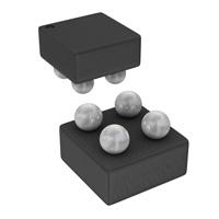
Each device includes one high-level ESD protection diode in a 4-channel 0.4 mm
(IP438xCX4) or 0.5 mm (IP4085CX4) pitch Wafer Level Chip-Size Package (WLCSP).
The anode and the cathode of ESD protection diode are each connected to two solder
balls.
1.2 Features and benefits
Single integrated high-performance ESD protection diode
Surge immunity according to IEC 61000-4-5 (8/20 s) up to 60 A (IP4085CX4)
ESD protection of >30 kV contact discharge, far exceeding IEC 61000-4-2, level 4
Small 2 2 solder ball WLCSP package with 0.4 mm or 0.5 mm pitch
1.3 Applications
General-purpose ESD protection such as for charger interfaces in:
Mobile handsets
Portable devices
Wireless data systems
�IP4085/4385/4386/4387/CX4
NXP Semiconductors
Integrated high-performance ESD protection diodes
2. Pinning information
Table 1.
Pin
Pinning
Description
Simplified outline
Graphic symbol
A1 and A2 cathode
B1 and B2 anode
A1
bump A1
index area
1
2
B1
A2
B2
006aad220
A
B
008aaa236
transparent top view,
solder balls facing down
3. Ordering information
Table 2.
Ordering information
Type number
IP4085CX4/LF/P
Package
Name
Description
WLCSP4
IP4385CX4/LF
Version
wafer level chip-size package: 4 bumps (2
2)[1]
IP4085CX4/LF/P
wafer level chip-size package: 4 bumps (2
2)[2]
IP4385CX4/LF
IP4386CX4/P
IP4386CX4/P
IP4387CX4/P
IP4387CX4/P
[1]
Size: 0.91 0.91 0.65 mm
[2]
Size: 0.76 0.76 0.61 mm
IP4085_4385_4386_4387_CX4
All information provided in this document is subject to legal disclaimers.
Product data sheet
Rev. 2 — 14 December 2012
© NXP B.V. 2012. All rights reserved.
2 of 18
�IP4085/4385/4386/4387/CX4
NXP Semiconductors
Integrated high-performance ESD protection diodes
4. Limiting values
Table 3.
Limiting values
In accordance with the Absolute Maximum Rating System (IEC 60134).
Symbol
Parameter
Conditions
Min
Max
Unit
VRWM
reverse standoff voltage
IP4085CX4; IP4386CX4
0.5
+14
V
IP4385CX4
0.5
+5.5
V
IP4387CX4
0.5
+8.0
V
VESD
electrostatic discharge voltage
all pins to ground
contact discharge
[1]
30
+30
kV
air discharge
[1]
15
+15
kV
contact discharge
8
+8
kV
air discharge
15
+15
kV
IP4085CX4
60
-
A
IP4385CX4; IP4387CX4
33
-
A
IP4386CX4
28
-
A
IP4085CX4; IP4386CX4;
tp = 2 ms
10
-
A
IP4085CX4; IP4386CX4;
tp = 5 ms
8.5
-
A
IP4085CX4; IP4386CX4;
tp = 100 ms
3.5
-
A
IP4385CX4; IP4387CX4;
tp = 2 ms
11
-
A
IP4385CX4; IP4387CX4;
tp = 5 ms
9
-
A
IP4385CX4; IP4387CX4;
tp = 100 ms
5
-
A
IEC 61000-4-2, level 4;
all pins to ground
IEC 61000-4-5; tp = 8/20 s
peak pulse current
IPP
IFSM
non-repetitive peak forward
current
total power dissipation
Ptot
Tstg
storage temperature
Treflow(peak)
peak reflow temperature
Tamb
ambient temperature
10 pulses; 1 pulse per
second
forward conducting
[2]
IP4085CX4
[3]
-
1
W
IP4385CX4; IP4386CX4;
IP4387CX4
[3]
-
0.7
W
55
+150
C
-
260
C
30
+85
C
tp 10 s
[1]
Device tested with over 1000 pulses of 30 kV contact discharges, according to the IEC 61000-4-2 model.
[2]
Severe self-heating demands a heat-dissipation optimized Printed-Circuit Board (PCB) to prevent the device from de-soldering. For
ambient temperature above 50 C, the guaranteed life time is 48 hours at 0.7 W, assuming Rth to be 130 K/W as specified in Table 4.
[3]
Permanent operation at maximum power dissipation and above maximum junction temperature will result in a reduced life time.
IP4085_4385_4386_4387_CX4
All information provided in this document is subject to legal disclaimers.
Product data sheet
Rev. 2 — 14 December 2012
© NXP B.V. 2012. All rights reserved.
3 of 18
�IP4085/4385/4386/4387/CX4
NXP Semiconductors
Integrated high-performance ESD protection diodes
5. Thermal characteristics
Table 4.
Symbol
Rth(j-a)
[1]
Thermal characteristics
Parameter
thermal resistance from junction
to ambient
Conditions
[1]
on a 2-layer PCB
Typ
Unit
130
K/W
Depends on details of PCB layout.
6. Characteristics
Table 5.
Electrical characteristics
Tamb = 25 C; unless otherwise specified.
Symbol
Parameter
Conditions
VBR
breakdown voltage
IR = 15 mA
VCL
IRM
Cd
VF
clamping voltage
Min
Typ
Max
Unit
IP4085CX4; IP4386CX4
16
-
-
V
IP4385CX4
7.0
-
-
V
IP4387CX4
10
-
-
V
IP4085CX4
-
-
20
V
IP4385CX4
-
-
10
V
IP4386CX4
-
-
20
V
IP4387CX4
-
-
13
V
IP4085CX4; IP4385CX4
VR = +5 V
-
-
200
nA
IP4386CX4; VR = +14 V
-
-
200
nA
IP4387CX4; VR = +8 V
-
-
800
nA
IP4085CX4
-
180
-
pF
IP4385CX4
-
450
-
pF
IP4386CX4
-
160
-
pF
IP4387CX4
-
290
-
pF
[1]
-
-
1.15
V
[2]
-
-
1.3
V
[1]
-
-
1.0
V
[2]
-
-
1.1
V
[1]
-
-
1.15
V
[2]
-
-
1.3
V
[1]
-
-
1.10
V
[2]
-
-
1.25
V
IR = 1 A; Tamb 85 C at surge peak
pulse, according to IEC 61000-4-5
reverse leakage current
diode capacitance
forward voltage
VR = 0 V; f = 1 MHz
IF = 850 mA
IP4085CX4
IP4385CX4
IP4386CX4
IP4387CX4
[1]
Tamb +25 C
[2]
30 C Tamb +85 C
IP4085_4385_4386_4387_CX4
All information provided in this document is subject to legal disclaimers.
Product data sheet
Rev. 2 — 14 December 2012
© NXP B.V. 2012. All rights reserved.
4 of 18
�IP4085/4385/4386/4387/CX4
NXP Semiconductors
Integrated high-performance ESD protection diodes
7. Application information
7.1 Forward current DC clamping voltage
The forward current DC clamping voltage is an indicator of protection level of circuit from
voltage sources with the wrong polarity. Figure 1 shows basic measurement setup.
VCL
IF
V
006aad221
Fig 1.
Measuring DC clamping voltage with forward current
001aaj241
1.1
VCL
(V)
001aaj242
1.1
VCL
(V)
(1)
1.0
1.0
(1)
(2)
(2)
0.9
0.9
(3)
(3)
0.8
0.8
0.7
0.7
0
0.2
0.4
0.6
0.8
1.0
0
0.2
IF (A)
(1) Tamb = +25 C
(2) Tamb = +85 C
(2) Tamb = +85 C
(3) Tamb = 30 C
(3) Tamb = 30 C
IP4085CX4: DC clamping voltage as a function
of forward current
0.6
0.8
1.0
IF (A)
(1) Tamb = +25 C
Fig 2.
0.4
Fig 3.
IP4385CX4: DC clamping voltage as a function
of forward current
IP4085_4385_4386_4387_CX4
All information provided in this document is subject to legal disclaimers.
Product data sheet
Rev. 2 — 14 December 2012
© NXP B.V. 2012. All rights reserved.
5 of 18
�IP4085/4385/4386/4387/CX4
NXP Semiconductors
Integrated high-performance ESD protection diodes
001aaj243
1.1
VCL
(V)
VCL
(V)
(1)
1.0
001aaj244
1.1
(1)
1.0
(2)
(2)
(3)
0.9
0.9
(3)
0.8
0.8
0.7
0.7
0
0.2
0.4
0.6
0.8
1.0
0
0.2
IF (A)
(1) Tamb = +25 C
(2) Tamb = +85 C
(2) Tamb = +85 C
(3) Tamb = 30 C
(3) Tamb = 30 C
IP4386CX4: DC clamping voltage as a function
of forward current
0.6
0.8
1.0
IF (A)
(1) Tamb = +25 C
Fig 4.
0.4
Fig 5.
IP4387CX4: DC clamping voltage as a function
of forward current
IP4085_4385_4386_4387_CX4
All information provided in this document is subject to legal disclaimers.
Product data sheet
Rev. 2 — 14 December 2012
© NXP B.V. 2012. All rights reserved.
6 of 18
�IP4085/4385/4386/4387/CX4
NXP Semiconductors
Integrated high-performance ESD protection diodes
7.2 Peak clamping voltage
The peak clamping voltage for forward and reverse current pulses of 8/20 s
(IEC 61000-4-5) is an indicator of protection level of circuits from power surges due to
voltage discharges. The current pulse shape over time is shown in Figure 7. The basic
measurement setup for forward current and reverse current pulses respectively are
shown in Figure 6 and Figure 12.
VCL
V
IPP
006aad227
Fig 6.
Measuring peak clamping voltage with forward current
001aaj558
120
100 % IPP; 8 μs
IPP
(%)
80
e−t
50 % IPP; 20 μs
40
0
0
10
20
30
40
t (μs)
Fig 7.
8/20 s current pulse waveform according to IEC 61000-4-5
IP4085_4385_4386_4387_CX4
All information provided in this document is subject to legal disclaimers.
Product data sheet
Rev. 2 — 14 December 2012
© NXP B.V. 2012. All rights reserved.
7 of 18
�IP4085/4385/4386/4387/CX4
NXP Semiconductors
Integrated high-performance ESD protection diodes
006aad222
17
VCL
(V)
006aad223
20
VCL
(V)
15
(3)
16
(1)
13
(3)
(2)
11
12
9
(1)
(2)
8
7
20
28
36
44
20
28
36
IF (A)
(1) Tamb = +25 C
(1) Tamb = +25 C
(2) Tamb = +85 C
(2) Tamb = +85 C
(3) Tamb = 30 C
(3) Tamb = 30 C
Fig 8.
IP4085CX4: peak clamping voltage as a
function of forward current
006aad224
20
(3)
(2)
(1)
VCL
(V)
44
IF (A)
Fig 9.
IP4385CX4: peak clamping voltage as a
function of forward current
006aad225
20
VCL
(V)
16
16
12
12
(2)
(3)
(1)
8
8
20
28
36
44
20
IF (A)
28
36
44
IF (A)
(1) Tamb = +25 C
(1) Tamb = +25 C
(2) Tamb = +85 C
(2) Tamb = +85 C
(3) Tamb = 30 C
(3) Tamb = 30 C
Fig 10. IP4386CX4: peak clamping voltage as a
function of forward current
Fig 11. IP4387CX4: peak clamping voltage as a
function of forward current
IP4085_4385_4386_4387_CX4
All information provided in this document is subject to legal disclaimers.
Product data sheet
Rev. 2 — 14 December 2012
© NXP B.V. 2012. All rights reserved.
8 of 18
�IP4085/4385/4386/4387/CX4
NXP Semiconductors
Integrated high-performance ESD protection diodes
VCL
V
IPP
006aad226
Fig 12. Measuring peak clamping voltage with reverse current
006aad228
19
VCL
(V)
(2)
VCL
(V)
006aad229
8.75
8.50
(2)
18
8.25
(1)
(1)
8.00
(3)
17
(3)
7.75
16
0.2
0.4
0.6
0.8
1.0
1.2
1.4
IR (A)
1.6
7.50
0.4
0.8
1.2
1.6
IR (A)
(1) Tamb = +25 C
(1) Tamb = +25 C
(2) Tamb = +85 C
(2) Tamb = +85 C
(3) Tamb = 30 C
(3) Tamb = 30 C
Fig 13. IP4085CX4: peak clamping voltage as a
function of reverse current
Fig 14. IP4385CX4: peak clamping voltage as a
function of reverse current
IP4085_4385_4386_4387_CX4
All information provided in this document is subject to legal disclaimers.
Product data sheet
Rev. 2 — 14 December 2012
© NXP B.V. 2012. All rights reserved.
9 of 18
�IP4085/4385/4386/4387/CX4
NXP Semiconductors
Integrated high-performance ESD protection diodes
006aad230
19
VCL
(V)
006aad231
12.2
(2)
VCL
(V)
(2)
18
11.8
(1)
(1)
17
11.4
(3)
(3)
16
0.3
0.7
1.1
1.5
11.0
0.4
0.8
IR (A)
1.2
1.6
IR (A)
(1) Tamb = +25 C.
(1) Tamb = +25 C.
(2) Tamb = +85 C.
(2) Tamb = +85 C.
(3) Tamb = 30 C.
(3) Tamb = 30 C.
Fig 15. IP4386CX4: peak clamping voltage as a
function of reverse current
Fig 16. IP4387CX4: peak clamping voltage as a
function of reverse current
Measurements are done on a heat-dissipation optimized PCB with massive copper area
under the Device Under Test (DUT).
IP4085_4385_4386_4387_CX4
All information provided in this document is subject to legal disclaimers.
Product data sheet
Rev. 2 — 14 December 2012
© NXP B.V. 2012. All rights reserved.
10 of 18
�IP4085/4385/4386/4387/CX4
NXP Semiconductors
Integrated high-performance ESD protection diodes
8. Package outline
WLCSP4: wafer level chip-size package; 4 bumps (2 x 2)
D
bump A1
index area
A2
A
E
A1
detail X
e
b
B
e
A
1
2
X
European
projection
wlcsp4_2x2_po
Fig 17. Package outline WLCSP4
Table 6.
Package outline dimensions of IP4085CX4 (WLCSP4)
Symbol
Min
Typ
Max
Unit
A
0.60
0.65
0.70
mm
A1
0.22
0.24
0.26
mm
A2
0.38
0.41
0.44
mm
b
0.27
0.32
0.37
mm
D
0.86
0.91
0.96
mm
E
0.86
0.91
0.96
mm
e
0.5
0.5
0.5
mm
IP4085_4385_4386_4387_CX4
All information provided in this document is subject to legal disclaimers.
Product data sheet
Rev. 2 — 14 December 2012
© NXP B.V. 2012. All rights reserved.
11 of 18
�IP4085/4385/4386/4387/CX4
NXP Semiconductors
Integrated high-performance ESD protection diodes
Table 7.
Package outline dimensions of IP438xCX4 (WLCSP4)
Symbol
Min
Typ
Max
Unit
A
0.56
0.61
0.66
mm
A1
0.18
0.20
0.22
mm
A2
0.38
0.41
0.44
mm
b
0.21
0.26
0.31
mm
D
0.71
0.76
0.76
mm
E
0.71
0.76
0.81
mm
e
0.4
0.4
0.4
mm
9. Design and assembly recommendations
9.1 PCB design guidelines
For optimum performance, use a Non-Solder Mask Defined (NSMD), also known as a
copper-defined design, incorporating laser-drilled micro-vias connecting the ground pads
to a buried ground-plane layer. This results in the lowest possible ground inductance and
provides the best high frequency and ESD performance. Refer to Table 8 for the
recommended PCB design parameters.
Table 8.
Recommended PCB design parameters
Parameter
Value or Specification
PCB pad diameter
200 m
Micro-via diameter
100 m (0.004 inch)
Solder mask aperture diameter
370 m
Copper thickness
20 m to 40 m
Copper finish
AuNi
PCB material
FR4
9.2 PCB assembly guidelines for Pb-free soldering
Table 9.
Assembly recommendations
Parameter
Value or Specification
Solder screen aperture diameter
330 m
Solder screen thickness
100 m (0.004 inch)
Solder paste: Pb-free
SnAg (3 % to 4 %) Cu (0.5 % to 0.9 %)
Solder to flux ratio
50 : 50
Solder reflow profile
see Figure 18
IP4085_4385_4386_4387_CX4
All information provided in this document is subject to legal disclaimers.
Product data sheet
Rev. 2 — 14 December 2012
© NXP B.V. 2012. All rights reserved.
12 of 18
�IP4085/4385/4386/4387/CX4
NXP Semiconductors
Integrated high-performance ESD protection diodes
T
(°C)
Treflow(peak)
250
230
cooling rate
217
preheat
t1
t (s)
t2
t3
t4
t5
001aai943
The device is capable of withstanding at least three reflows of this profile.
Fig 18. Pb-free solder reflow profile
Table 10.
Symbol
Reflow soldering process characteristics
Parameter
Conditions
Treflow(peak) peak reflow temperature
Min
Typ
Max
Unit
230
-
260
C
-
180
s
t1
time 1
soak time
60
t2
time 2
time during T 250 C
-
-
30
s
t3
time 3
time during T 230 C
10
-
50
s
t4
time 4
time during T > 217 C
30
-
150
s
t5
time 5
-
-
540
s
dT/dt
rate of change of
temperature
cooling rate
-
-
6
C/s
pre-heat
2.5
-
4.0
C/s
IP4085_4385_4386_4387_CX4
All information provided in this document is subject to legal disclaimers.
Product data sheet
Rev. 2 — 14 December 2012
© NXP B.V. 2012. All rights reserved.
13 of 18
�IP4085/4385/4386/4387/CX4
NXP Semiconductors
Integrated high-performance ESD protection diodes
10. Soldering
D
e
c
(4×)
e
solder resist
E
solder paste = solderland
f
(4×)
occupied area
Dimensions in mm
wlcsp4_2x2_fr
Fig 19. Reflow soldering footprint WLCSP4
Table 11.
Soldering dimensions of IP4085CX4 (WLCSP4)
Symbol
Min
Typ
Max
Unit
c
-
0.31
-
mm
D
0.86
0.91
0.96
mm
E
0.86
0.91
0.96
mm
e
-
0.5
-
mm
f
-
0.385
-
mm
Table 12.
Soldering dimensions of IP438xCX4 (WLCSP4)
Symbol
Min
Typ
Max
Unit
c
-
0.25
-
mm
D
0.71
0.76
0.81
mm
E
0.71
0.76
0.81
mm
e
-
0.4
-
mm
f
-
0.325
-
mm
IP4085_4385_4386_4387_CX4
All information provided in this document is subject to legal disclaimers.
Product data sheet
Rev. 2 — 14 December 2012
© NXP B.V. 2012. All rights reserved.
14 of 18
�IP4085/4385/4386/4387/CX4
NXP Semiconductors
Integrated high-performance ESD protection diodes
11. Revision history
Table 13.
Revision history
Document ID
Release
date
Data sheet status
Change Supersedes
notice
IP4085_4385_4386_4387_CX4 v.2
20121214
Product data sheet
-
Modifications:
IP4085_4385_4386_4387_CX4 v.1
•
•
•
•
•
•
•
•
•
•
•
•
IP4085_4385_4386_4387_CX4 v.1
Basic type IP4085CX4/LF removed
Section 1 “Product profile”: updated
Section 2 “Pinning information”: updated
Functional diagram: removed
Table 3 “Limiting values”: updated
Table 5 “Electrical characteristics”. updated
Section 7 “Application information”. updated
Figure 1, 6, 8 to 16: updated
Marking: removed
Section 8 “Package outline”: updated
Section 10 “Soldering”: added
Section 12 “Legal information”: updated
20090326
Product data sheet
-
IP4085_4385_4386_4387_CX4
All information provided in this document is subject to legal disclaimers.
Product data sheet
Rev. 2 — 14 December 2012
-
© NXP B.V. 2012. All rights reserved.
15 of 18
�IP4085/4385/4386/4387/CX4
NXP Semiconductors
Integrated high-performance ESD protection diodes
12. Legal information
12.1 Data sheet status
Document status[1][2]
Product status[3]
Definition
Objective [short] data sheet
Development
This document contains data from the objective specification for product development.
Preliminary [short] data sheet
Qualification
This document contains data from the preliminary specification.
Product [short] data sheet
Production
This document contains the product specification.
[1]
Please consult the most recently issued document before initiating or completing a design.
[2]
The term ‘short data sheet’ is explained in section “Definitions”.
[3]
The product status of device(s) described in this document may have changed since this document was published and may differ in case of multiple devices. The latest product status
information is available on the Internet at URL http://www.nxp.com.
12.2 Definitions
Draft — The document is a draft version only. The content is still under
internal review and subject to formal approval, which may result in
modifications or additions. NXP Semiconductors does not give any
representations or warranties as to the accuracy or completeness of
information included herein and shall have no liability for the consequences of
use of such information.
Short data sheet — A short data sheet is an extract from a full data sheet
with the same product type number(s) and title. A short data sheet is intended
for quick reference only and should not be relied upon to contain detailed and
full information. For detailed and full information see the relevant full data
sheet, which is available on request via the local NXP Semiconductors sales
office. In case of any inconsistency or conflict with the short data sheet, the
full data sheet shall prevail.
Product specification — The information and data provided in a Product
data sheet shall define the specification of the product as agreed between
NXP Semiconductors and its customer, unless NXP Semiconductors and
customer have explicitly agreed otherwise in writing. In no event however,
shall an agreement be valid in which the NXP Semiconductors product is
deemed to offer functions and qualities beyond those described in the
Product data sheet.
12.3 Disclaimers
Limited warranty and liability — Information in this document is believed to
be accurate and reliable. However, NXP Semiconductors does not give any
representations or warranties, expressed or implied, as to the accuracy or
completeness of such information and shall have no liability for the
consequences of use of such information. NXP Semiconductors takes no
responsibility for the content in this document if provided by an information
source outside of NXP Semiconductors.
In no event shall NXP Semiconductors be liable for any indirect, incidental,
punitive, special or consequential damages (including - without limitation - lost
profits, lost savings, business interruption, costs related to the removal or
replacement of any products or rework charges) whether or not such
damages are based on tort (including negligence), warranty, breach of
contract or any other legal theory.
Notwithstanding any damages that customer might incur for any reason
whatsoever, NXP Semiconductors’ aggregate and cumulative liability towards
customer for the products described herein shall be limited in accordance
with the Terms and conditions of commercial sale of NXP Semiconductors.
Right to make changes — NXP Semiconductors reserves the right to make
changes to information published in this document, including without
limitation specifications and product descriptions, at any time and without
notice. This document supersedes and replaces all information supplied prior
to the publication hereof.
Suitability for use — NXP Semiconductors products are not designed,
authorized or warranted to be suitable for use in life support, life-critical or
safety-critical systems or equipment, nor in applications where failure or
malfunction of an NXP Semiconductors product can reasonably be expected
to result in personal injury, death or severe property or environmental
damage. NXP Semiconductors and its suppliers accept no liability for
inclusion and/or use of NXP Semiconductors products in such equipment or
applications and therefore such inclusion and/or use is at the customer’s own
risk.
Applications — Applications that are described herein for any of these
products are for illustrative purposes only. NXP Semiconductors makes no
representation or warranty that such applications will be suitable for the
specified use without further testing or modification.
Customers are responsible for the design and operation of their applications
and products using NXP Semiconductors products, and NXP Semiconductors
accepts no liability for any assistance with applications or customer product
design. It is customer’s sole responsibility to determine whether the NXP
Semiconductors product is suitable and fit for the customer’s applications and
products planned, as well as for the planned application and use of
customer’s third party customer(s). Customers should provide appropriate
design and operating safeguards to minimize the risks associated with their
applications and products.
NXP Semiconductors does not accept any liability related to any default,
damage, costs or problem which is based on any weakness or default in the
customer’s applications or products, or the application or use by customer’s
third party customer(s). Customer is responsible for doing all necessary
testing for the customer’s applications and products using NXP
Semiconductors products in order to avoid a default of the applications and
the products or of the application or use by customer’s third party
customer(s). NXP does not accept any liability in this respect.
Limiting values — Stress above one or more limiting values (as defined in
the Absolute Maximum Ratings System of IEC 60134) will cause permanent
damage to the device. Limiting values are stress ratings only and (proper)
operation of the device at these or any other conditions above those given in
the Recommended operating conditions section (if present) or the
Characteristics sections of this document is not warranted. Constant or
repeated exposure to limiting values will permanently and irreversibly affect
the quality and reliability of the device.
Terms and conditions of commercial sale — NXP Semiconductors
products are sold subject to the general terms and conditions of commercial
sale, as published at http://www.nxp.com/profile/terms, unless otherwise
agreed in a valid written individual agreement. In case an individual
agreement is concluded only the terms and conditions of the respective
agreement shall apply. NXP Semiconductors hereby expressly objects to
applying the customer’s general terms and conditions with regard to the
purchase of NXP Semiconductors products by customer.
No offer to sell or license — Nothing in this document may be interpreted or
construed as an offer to sell products that is open for acceptance or the grant,
conveyance or implication of any license under any copyrights, patents or
other industrial or intellectual property rights.
IP4085_4385_4386_4387_CX4
All information provided in this document is subject to legal disclaimers.
Product data sheet
Rev. 2 — 14 December 2012
© NXP B.V. 2012. All rights reserved.
16 of 18
�IP4085/4385/4386/4387/CX4
NXP Semiconductors
Integrated high-performance ESD protection diodes
Export control — This document as well as the item(s) described herein
may be subject to export control regulations. Export might require a prior
authorization from competent authorities.
Quick reference data — The Quick reference data is an extract of the
product data given in the Limiting values and Characteristics sections of this
document, and as such is not complete, exhaustive or legally binding.
Non-automotive qualified products — Unless this data sheet expressly
states that this specific NXP Semiconductors product is automotive qualified,
the product is not suitable for automotive use. It is neither qualified nor tested
in accordance with automotive testing or application requirements. NXP
Semiconductors accepts no liability for inclusion and/or use of
non-automotive qualified products in automotive equipment or applications.
In the event that customer uses the product for design-in and use in
automotive applications to automotive specifications and standards, customer
(a) shall use the product without NXP Semiconductors’ warranty of the
product for such automotive applications, use and specifications, and (b)
whenever customer uses the product for automotive applications beyond
NXP Semiconductors’ specifications such use shall be solely at customer’s
own risk, and (c) customer fully indemnifies NXP Semiconductors for any
liability, damages or failed product claims resulting from customer design and
use of the product for automotive applications beyond NXP Semiconductors’
standard warranty and NXP Semiconductors’ product specifications.
12.4 Trademarks
Notice: All referenced brands, product names, service names and trademarks
are the property of their respective owners.
13. Contact information
For more information, please visit: http://www.nxp.com
For sales office addresses, please send an email to: salesaddresses@nxp.com
IP4085_4385_4386_4387_CX4
All information provided in this document is subject to legal disclaimers.
Product data sheet
Rev. 2 — 14 December 2012
© NXP B.V. 2012. All rights reserved.
17 of 18
�NXP Semiconductors
IP4085/4385/4386/4387/CX4
Integrated high-performance ESD protection diodes
14. Contents
1
1.1
1.2
1.3
2
3
4
5
6
7
7.1
7.2
8
9
9.1
9.2
10
11
12
12.1
12.2
12.3
12.4
13
14
Product profile . . . . . . . . . . . . . . . . . . . . . . . . . . 1
General description . . . . . . . . . . . . . . . . . . . . . 1
Features and benefits . . . . . . . . . . . . . . . . . . . . 1
Applications . . . . . . . . . . . . . . . . . . . . . . . . . . . 1
Pinning information . . . . . . . . . . . . . . . . . . . . . . 2
Ordering information . . . . . . . . . . . . . . . . . . . . . 2
Limiting values. . . . . . . . . . . . . . . . . . . . . . . . . . 3
Thermal characteristics . . . . . . . . . . . . . . . . . . 4
Characteristics . . . . . . . . . . . . . . . . . . . . . . . . . . 4
Application information. . . . . . . . . . . . . . . . . . . 5
Forward current DC clamping voltage . . . . . . . 5
Peak clamping voltage . . . . . . . . . . . . . . . . . . . 7
Package outline . . . . . . . . . . . . . . . . . . . . . . . . 11
Design and assembly recommendations . . . 12
PCB design guidelines . . . . . . . . . . . . . . . . . . 12
PCB assembly guidelines for Pb-free
soldering . . . . . . . . . . . . . . . . . . . . . . . . . . . . . 12
Soldering . . . . . . . . . . . . . . . . . . . . . . . . . . . . . 14
Revision history . . . . . . . . . . . . . . . . . . . . . . . . 15
Legal information. . . . . . . . . . . . . . . . . . . . . . . 16
Data sheet status . . . . . . . . . . . . . . . . . . . . . . 16
Definitions . . . . . . . . . . . . . . . . . . . . . . . . . . . . 16
Disclaimers . . . . . . . . . . . . . . . . . . . . . . . . . . . 16
Trademarks. . . . . . . . . . . . . . . . . . . . . . . . . . . 17
Contact information. . . . . . . . . . . . . . . . . . . . . 17
Contents . . . . . . . . . . . . . . . . . . . . . . . . . . . . . . 18
Please be aware that important notices concerning this document and the product(s)
described herein, have been included in section ‘Legal information’.
© NXP B.V. 2012.
All rights reserved.
For more information, please visit: http://www.nxp.com
For sales office addresses, please send an email to: salesaddresses@nxp.com
Date of release: 14 December 2012
Document identifier: IP4085_4385_4386_4387_CX4
�