GW VJLPE1.EM-K2K3-A333-1-350-R18 数据手册
www.osram-os.com
Produktdatenblatt | Version 1.1
GW VJLPE1.EM
GW VJLPE1.EM
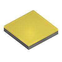
OSLON ® Pure 1010
Applications
——Downlights/Spotlights
Features:
——Typ. Radiation: 120° (Lambertian emitter)
——Color temperature: 2700K - 5000K
——CRI: 80 (min.)
——Luminous Flux: typ. 100 lm @ 3000 K, 85 °C
——Luminous efficacy: typ. 100 lm/W @ 3000 K, 85 °C
1 Version 1.0 | 2019-04-02
�GW VJLPE1.EM
Ordering Information
Type
Color temperature
Luminous Flux 1)
IF = 350 mA
ΦV
Ordering Code
GW VJLPE1.EM-KZLS-A838-1
2700 K
80 ... 105 lm
Q65112A7103
GW VJLPE1.EM-KSLT-A737-1
3000 K
85 ... 110 lm
Q65112A7105
GW VJLPE1.EM-K2K3-A535-1
4000 K
95 ... 120 lm
Q65112A7106
GW VJLPE1.EM-K2K3-A333-1
5000 K
95 ... 120 lm
Q65112A7107
2 Version 1.0 | 2019-04-02
�GW VJLPE1.EM
Maximum Ratings
Parameter
Symbol
Operating Temperature
Top
min.
max.
-40 °C
100 °C
Storage Temperature
Tstg
min.
max.
-40 °C
100 °C
Junction Temperature
Tj
max.
125 °C
Forward Current
TJ = 85 °C
IF
min.
max.
20 mA
700 mA
Reverse voltage 2)
VR
ESD withstand voltage
acc. ANSI/ESDA/JEDEC JS-001 (HBM, Class 0)
VESD
3 Version 1.0 | 2019-04-02
Values
Not designed for
reverse operation
ESD sensitive device
�GW VJLPE1.EM
Characteristics
IF = 350 mA; TJ = 85 °C
Parameter
Symbol
Viewing angle at 50% IV
2φ
typ.
120 °
Forward Voltage 3)
VF
min.
typ.
max.
2.70 V
2.80 V
3.20 V
Reverse current 2)
IR
Color Rendering Index 4)
CRI
min.
80
Electrical thermal resistance junction/solderpoint
with efficiency ηe = 31 %
RthJS elec.
typ.
7.2 K / W
4 Version 1.0 | 2019-04-02
Values
Not designed
for reverse
operation
�GW VJLPE1.EM
Brightness Groups
Group
Luminous Flux 1)
IF = 350 mA
min.
ΦV
Luminous Flux 1)
IF = 350 mA
max.
ΦV
KZ
80 lm
85 lm
KS
85 lm
90 lm
K1
90 lm
95 lm
K2
95 lm
100 lm
LS
100 lm
105 lm
LT
105 lm
110 lm
LU
110 lm
115 lm
K3
115 lm
120 lm
Forward Voltage Groups
Forward Voltage 3)
min.
VF
Forward Voltage 3)
max.
VF
K2
2.70 V
2.80 V
L1
2.80 V
2.90 V
L2
2.90 V
3.00 V
M1
3.00 V
3.10 V
M2
3.10 V
3.20 V
Group
5 Version 1.0 | 2019-04-02
�GW VJLPE1.EM
Chromaticity Coordinate Groups
6 Version 1.0 | 2019-04-02
5)
�GW VJLPE1.EM
Chromaticity Coordinate Groups
CCT
Center
Cx
Center
Cy
3step
a
3step
b
5step
a
5step
b
Ø
2200 K
0.5020
0.4156
0.0072
0.0040
0.0120
0.0067
39.9
2700 K
0.4577
0.4098
0.0080
0.0041
0.0133
0.0068
54.1
3000 K
0.4339
0.4032
0.0086
0.0042
0.0142
0.0069
53.7
4000 K
0.3818
0.3796
0.0094
0.0041
0.0157
0.0068
53.4
5000 K
0.3446
0.3551
0.0081
0.0035
0.0135
0.0059
59.8
7 Version 1.0 | 2019-04-02
�GW VJLPE1.EM
1
CCT
2200 K
2700 K
3000 K
3
4
5
Group
Cx
Cy
Cx
Cy
Cx
Cy
Cx
Cy
Cx
Cy
A
0.5155
0.4347
0.5044
0.4344
0.4921
0.4156
0.4941
0.4156
0.5088
0.4249
B
0.5155
0.4347
0.5265
0.4350
0.5132
0.4163
0.5101
0.4161
0.5088
0.4249
C
0.5132
0.4163
0.4998
0.3975
0.4898
0.3971
0.4955
0.4054
0.5101
0.4161
D
0.4955
0.4054
0.4941
0.4156
0.4921
0.4156
0.4798
0.3967
0.4898
0.3971
E
0.5088
0.4249
0.4941
0.4156
0.4973
0.4157
0.5061
0.4210
F
0.5088
0.4249
0.5101
0.4161
0.5068
0.4160
0.5061
0.4210
G
0.5101
0.4161
0.4955
0.4054
0.4981
0.4093
0.5068
0.4158
H
0.4981
0.4093
0.4973
0.4157
0.4941
0.4156
0.4955
0.4054
A
0.4675
0.4285
0.4561
0.4259
0.4467
0.4076
0.4491
0.4081
0.4637
0.4212
B
0.4675
0.4285
0.4811
0.4315
0.4698
0.4123
0.4663
0.4115
0.4637
0.4212
C
0.4698
0.4123
0.4591
0.3941
0.4482
0.3917
0.4517
0.3984
0.4663
0.4115
D
0.4517
0.3984
0.4491
0.4081
0.4467
0.4076
0.4372
0.3892
0.4482
0.3917
E
0.4637
0.4212
0.4491
0.4081
0.4526
0.4088
0.4613
0.4166
F
0.4637
0.4212
0.4663
0.4115
0.4628
0.4108
0.4613
0.4166
G
0.4663
0.4115
0.4517
0.3984
0.4541
0.4030
0.4628
0.4108
H
0.4541
0.4030
0.4526
0.4088
0.4491
0.4081
0.4517
0.3984
A
0.4418
0.4211
0.4302
0.4171
0.4226
0.3995
0.4246
0.4002
0.4393
0.4153
B
0.4418
0.4211
0.4561
0.4259
0.4465
0.4073
0.4432
0.4062
0.4393
0.4153
C
0.4465
0.4073
0.4372
0.3892
0.4261
0.3856
0.4285
0.3911
0.4432
0.4062
D
0.4285
0.3911
0.4246
0.4002
0.4226
0.3995
0.4149
0.3819
0.4261
0.3856
E
0.4393
0.4153
0.4246
0.4002
0.4283
0.4014
0.4371
0.4105
F
0.4393
0.4153
0.4432
0.4062
0.4395
0.4050
0.4371
0.4105
G
0.4432
0.4062
0.4285
0.3911
0.4307
0.3960
0.4395
0.4050
H
0.4307
0.3960
0.4283
0.4014
0.4246
0.4002
0.4285
0.3911
A
0.3853
0.3947
0.3737
0.3879
0.3704
0.3731
0.3714
0.3737
0.3845
0.3913
B
0.3853
0.3947
0.4003
0.4034
0.3949
0.3871
0.3922
0.3855
0.3845
0.3913
C
0.3949
0.3871
0.3895
0.3707
0.3783
0.3645
0.3791
0.3679
0.3922
0.3855
D
0.3791
0.3679
0.3714
0.3737
0.3704
0.3731
0.3671
0.3583
0.3783
0.3645
E
0.3845
0.3913
0.3714
0.3737
0.3756
0.3760
0.3834
0.3866
F
0.3845
0.3913
0.3922
0.3855
0.3880
0.3832
0.3834
0.3866
G
0.3922
0.3855
0.3791
0.3679
0.3802
0.3726
0.3880
0.3832
H
0.3802
0.3726
0.3756
0.3760
0.3714
0.3737
0.3791
0.3679
4000 K
2
8 Version 1.0 | 2019-04-02
�GW VJLPE1.EM
5000 K
A
0.3452
0.3678
0.3375
0.3619
0.3372
0.3528
0.3451
0.3648
B
0.3452
0.3678
0.3550
0.3752
0.3532
0.3614
0.3530
0.3612
0.3451
0.3648
C
0.3532
0.3614
0.3514
0.3480
0.3440
0.3426
0.3441
0.3454
0.3530
0.3612
D
0.3441
0.3454
0.3369
0.3445
0.3366
0.3372
0.3440
0.3426
E
0.3451
0.3648
0.3372
0.3528
0.3371
0.3496
0.3396
0.3514
0.3449
0.3609
F
0.3451
0.3648
0.3530
0.3612
0.3496
0.3588
0.3449
0.3609
G
0.3530
0.3612
0.3441
0.3454
0.3443
0.3493
0.3496
0.3588
H
0.3443
0.3493
0.3396
0.3514
0.3371
0.3496
0.3369
0.3445
0.3441
0.3454
9 Version 1.0 | 2019-04-02
�GW VJLPE1.EM
Group Name on Label
Example: K1-K2
Brightness
Forward Voltage
K1
K2
10 Version 1.0 | 2019-04-02
�GW VJLPE1.EM
Relative Spectral Emission
6)
Φrel = f (λ); IF = 350 mA; TJ = 85 °C
Φrel
GW VJLPE1.EM
1,0
: Vλ
: white
0,8
0,6
0,4
0,2
0,0
350
400
450
500
550
600
650
700
750
Note: The radiation characteristics represent the emission of the chips only and do not
take into consideration a potential shadowing by the connector
Radiation Characteristics
800
λ / nm
6)
Irel = f (ϕ); TJ = 85 °C
GW VJLPE1.EM
ϕ/°
-40°
-50°
-20°
-10°
0° 10° 20° 30° 40° 50° 60° 70° 80° 90°
1,0
-30°
0,8
0,6
-60°
-70°
0,4
0,2
-90°
0,0
-80°
11 Version 1.0 | 2019-04-02
Irel
�GW VJLPE1.EM
Forward current
Relative Luminous Flux
6), 7)
IF = f(VF); TJ = 85 °C
IF / mA
6), 7)
Φv/Φv(350 mA) = f(IF); TJ = 85 °C
GW VJLPE1.EM
700
ΦV
GW VJLPE1.EM
1,8
ΦV(350mA)
1,6
600
1,4
500
1,2
400
1,0
0,8
300
0,6
200
0,4
100
Chromaticity Coordinate Shift
6)
ΔCx, ΔCy = f(IF); TJ = 85 °C
∆Cx
∆Cy
GW VJLPE1.EM
0,02
: ∆ Cx
: ∆ Cy
0,01
0,00
-0,01
70
0
60
0
50
0
40
0
30
0
20
0
10
0
20
-0,02
IF / mA
12 Version 1.0 | 2019-04-02
70
0
60
0
50
0
40
0
2,85 2,89
VF / V
30
0
2,80
20
0
2,75
20
2,70
10
0
0,2
20
2,65
IF / mA
�GW VJLPE1.EM
Forward Voltage
Relative Luminous Flux
6)
ΔVF = VF - VF(85 °C) = f(Tj); IF = 350 mA
∆VF / V
0,3
6)
Φv/Φv(85 °C) = f(Tj); IF = 350 mA
GW VJLPE1.EM
Φv
1,4
GW VJLPE1.EM
Φv(85°C)
1,2
0,2
1,0
0,8
0,1
0,6
0,4
0,0
0,2
-0,1
-40 -20 0
20 40 60 80 100 120
Tj / °C
Chromaticity Coordinate Shift
6)
ΔCx, ΔCy = f(Tj); IF = 350 mA
∆Cx
∆Cy
0,02
0,01
GW VJLPE1.EM
: ∆ Cx
: ∆ Cy
0,00
-0,01
20 40 60 80 100 120
Tj / °C
-0,02
-40 -20 0
13 Version 1.0 | 2019-04-02
0,0
-40 -20 0
20 40 60 80 100 120
Tj / °C
�GW VJLPE1.EM
Max. Permissible Forward Current
IF = f(T)
IF / mA
GW VJLPE1.EM
800
700
600
500
400
300
200
100
0
0
Don't use below 20 mA
20
40
60
14 Version 1.0 | 2019-04-02
80
100
Ts / °C
�GW VJLPE1.EM
Dimensional Drawing
8)
Further Information
0.8 mg
Approximate Weight:
15 Version 1.0 | 2019-04-02
�GW VJLPE1.EM
Recommended Solder Pad
16 Version 1.0 | 2019-04-02
8)
�GW VJLPE1.EM
Reflow Soldering Profile
Product complies to MSL Level 2 acc. to JEDEC J-STD-020E
OHA04525
300
˚C
T 250
Tp 245 ˚C
240 ˚C
tP
217 ˚C
200
tL
150
tS
100
50
25 ˚C
0
0
50
100
150
200
250
s 300
t
Profile Feature
Symbol
Pb-Free (SnAgCu) Assembly
Minimum
Recommendation Maximum
Ramp-up rate to preheat*)
25 °C to 150 °C
tS
Time tS
TSmin to TSmax
Ramp-up rate to peak*)
TSmax to TP
Liquidus temperature
60
2
3
100
120
2
3
Unit
K/s
s
K/s
TL
217
Time above liquidus temperature
tL
80
100
s
Peak temperature
TP
245
260
°C
Time within 5 °C of the specified peak
temperature TP - 5 K
tP
20
30
3
6
Ramp-down rate*
TP to 100 °C
10
Time
25 °C to TP
All temperatures refer to the center of the package, measured on the top of the component
* slope calculation DT/Dt: Dt max. 5 s; fulfillment for the whole T-range
17 Version 1.0 | 2019-04-02
°C
480
s
K/s
s
�GW VJLPE1.EM
Taping
8)
18 Version 1.0 | 2019-04-02
�GW VJLPE1.EM
Tape and Reel
9)
Reel Dimensions
A
180 mm
W
Nmin
12 + 0.3 / - 0.1 mm
19 Version 1.0 | 2019-04-02
W1
60 mm
W2 max
12.4 + 2 mm
18.4 mm
Pieces per PU
600
�GW VJLPE1.EM
Barcode-Product-Label (BPL)
Dry Packing Process and Materials
8)
Moisture-sensitive label or print
L
E
E
V
l
e be
sela
).
k,
H
de
L
If
an
bl r co
ba
(R
id
m
ity
.
H
R
hu
0%
e
e
/6
tiv
˚C
la ared ag
ck
re
fr
30
_
<
in pa
%
k
of
to
90
rs
ea
s
d
).
rs
ou
or
te (p
on
rs
H
de
,
ou
iti
H
an bjec ng
ou rs
co
˚C
72
si
nd
H ou
5
te
48
˚C su es
e
H
co
±
24 6
da
e
y
40 be oc
tim
˚C
e
or
<
ith
tim
ill pr).
or
ct
w
O
w nt
23
tim e
at
lo
or
fa
M TO
F
s
al
tim
at le ˚C at
lo
at
or
e.
P
th
F
l
tic
th va
lo or
ur
O
F lo
s ui
on
be
if: read
en
w
ed
l 4 5
F
m
la
ce eq
id
lo
g, n
oc
l
ve
vi
5a
is
in
or
be
24
de
pr
ve l
6
Le
de ,
nt whe
e
te
co
g:
, w
e
Le ve l
ke
r
ou
se
da
ba ed flo
ur
e
Le ve
m %
ba
e
ba
al
st
ur e
Le
r
en re
ed
e
re> 10
oi
st
e
e
fo
tim
ur
se
al
op
fo
M
se
oi st ur
as
k,
is
or .
33
se
is
M oi st
bed
k,
lo H
an
,
g ph
-0
M oi
in
an in F R ng ar
rbl
D
M
e
ba
T
r
po If bl ith
%
lif
ki r C.
(if
S
is
p.
w
ea r ks
lf
J10 ba to et
th va
Y ea
m
rs
m
_
r w,
<
he
ed
1
ee
te
Y
d, EC
iredicat
S
fte
at
nt
>
1
W Hou
D
A flody
qu In no ire
1.
d
e
ou
4 8
re
reity is
qu/JE
re
2.
bo
e
M
tim
to es id 2b
re C
16
:
e
a)
S
tim
is IP
ic
ed loor
tim e
b) ev Humor
or
e
en
F
tim
lo
or
D
2a king
nc
te
F
op
a)
lo or
3.
b) ba re
F lo
da
e
fe
l 1 2
F
If
al
re
tim ve
l
4.
se
d
l 2a
ve
Le
3
an
ve l
ag
e
Le
e
B
ve
ur
e
Le
at
st
ur
e
Le
D
oi
st
ur e
M
oi
st ur
M
oi st
M oi
M
N
E RS
s
in IV O
IT T
S C
nta
N U
TIO
U coSEND
Ais bUagRMEICO
T E
CThIS
S
d
Barcode label
<
M
RA
OS
Humidity indicator
Barcode label
Please check the HIC immidiately after
bag opening.
Discard if circles overrun.
Avoid metal contact.
Do not eat.
Comparator
check dot
WET
If wet,
examine units, if necessary
bake units
15%
If wet,
examine units, if necessary
bake units
10%
5%
If wet,
parts still adequately dry.
change desiccant
Humidity Indicator
MIL-I-8835
Desiccant
AM
OSR
OHA00539
Moisture-sensitive product is packed in a dry bag containing desiccant and a humidity card according JEDEC-STD-033.
20 Version 1.0 | 2019-04-02
�GW VJLPE1.EM
Schematic Transportation Box
8)
Barcode label
N
O
:
(Q
)Q
TY
:2
00
0
(9
D
)
D
/C
:0
(X
)
Packing
Sealing label
Length
195 ± 5 mm
195 ± 5 mm
21 Version 1.0 | 2019-04-02
M
Y
DE
-1
+Q
-1
R
18
P
OHA02044
Dimensions of Transportation Box
Width
RO
UP
:
M
RA
OS
PR
O
D
5
14 2
110 0
G
4
01
4
C:
D/
(9
D)
20
00
(Q
)Q
TY
:
O
TC
P)
(6
T
LO
(1
T)
O
D
PR
D
EM
Y
18
R
-1
:
Q
+
P
-1
G
R
O
U
P:
u L
lt S
iT Y
O T6
P 7
L 6
M
14
4
(G
)
E Bi
D Bi n1
Bi n2 : Pn3 : Q 1: -1 20
M
-2
2 L
0
Te
2a
22 m
3
24 0 p ST
Ad 26 0 C R
C
R ditio 0 C R
07
PA 7 na RT
l TE
C
KV
XT
AR
Muster
A
o M
n O
d
u p
cto to
rs
R
34
ic
N
O
:
O
S
H
12
G
BA
TC
H
(1
T)
LO
T
N
O
:1
(6
P)
23
em
8
2199
2100
5
14 2
110 0
(X
)
O
M O
PT
O
M
998
NO
:
CThISTU
SE
S
21
2100
BA
_
<
s
ur s
).
Ho ururs s
de
Ho
co
72
Ho ur
te
48
e
Ho
24 6
da
40 be
tim e e
˚C
or
th
r
pr
<
ll
tim
ct
).
23
oo r
wi nt
tim e
at
l wi
fa
r
Fl oo
tim
s
at
at le ˚C at
e.
ica
l
Fl
th
oo r
th va
ur
nt
Fl oo
s ui
be
on
if: read
w
ed
l 4 5
Fl
la
m
ide
ce eq
lo
g,
oc
ve l
vi
is
in en
de
be
24 de or
l 5a6
pr
Le ve
nt wh
e
te
co
, w,
g:
ve l
Le
ke
r
re
ou
se
da
ba ed flo ba
Le ve
tu re
m %
ba
e
al
e
Le
r
en re
e
ed
re 10
ois stu ur e
tim
se
fo
al
op se
fo >
,
M oi
r
se
st ur
3
is
is ha
se
M
oi st
nk
be
k,
oo .
03
rd
g
M oi
in
an in Fl RH g,
r-p
bla
DM
ba
Ca
po If bl th
%
kinr
life is
(if
.
ar
ST
f
p.
wi
10 ba to et
Jel r th va
Ye ar ks s
m
_
<
cat m d, C
ed
1
Ye ee ur
ire
Sh te w, te
di
at
nt
>
1
W Ho
Af flody
qu In no ire DE
1.
e
ou
4 8
re
ed re
qu JE
2.
bo
ity is
M
or
tim e e
16
re C/
:
es id 2b
r
a)
St
tim
mor
is IP
ed
oo r
tim e
vic
b)
g e
r
Hu
Fl oo
en
tim
De
2a kin nc
te
Fl oo r
a)
op
3.
b) ba re
Fl oo
da
e
fe
l 1
Fl
If
al
re
tim ve l 2
4.
se
d
l 2a3
Le ve
g
an
ve l
e
Le
Ba
te
ur e
Le ve
Le
Da oist stur e
ur e
M
oi
st ur
M
oi st
M oi
H
12
34
.
RH
0%
/6
˚C
:
L
e el
selab
.
,
H)
nk de
co
(R
bla
r
S S
em R
ic AM
o
n O
d
u p
ct to
o
H
rs
NO
If
23
G
E
V
E
ba
ity
id
m
hu
e
e
d
tiv
re ag
NO
:1
L
la
re
fra ck
30
Nns IVE RS
in pa
%
k
of
ai IT TO
to
90
ea
d
ntNS
<
ns
UC
or
TIO
te (p
d
,
g
itio
ND
U g coSE
an bjec
˚C
sin
nd
O
5
˚C su es
Ais baRE
co
IC
±
y
M
oc
(G
)
M
u L
lt S
iT Y
O T6
P 7
L 6
E
D
Muster
Bi
Bi n1
Bi n2 : P-
n3 : Q 1: -1 20
M
-2
2 L
0
Te
2a
22 m
3
24 0 p ST
Ad 26 0 C R
C
R0 ditio 0 C R
PA 77 na RT
l TE
CK
VA
XT
R:
Barcode label
Height
30 ± 5 mm
�GW VJLPE1.EM
Notes
The evaluation of eye safety occurs according to the standard IEC 62471:2006 (photo biological safety of
lamps and lamp systems). Within the risk grouping system of this IEC standard, the device specified in this
data sheet falls into the class moderate risk (exposure time 0.25 s). Under real circumstances (for exposure
time, conditions of the eye pupils, observation distance), it is assumed that no endangerment to the eye exists from these devices. As a matter of principle, however, it should be mentioned that intense light sources
have a high secondary exposure potential due to their blinding effect. When looking at bright light sources
(e.g. headlights), temporary reduction in visual acuity and afterimages can occur, leading to irritation, annoyance, visual impairment, and even accidents, depending on the situation.
Subcomponents of this device contain, in addition to other substances, metal filled materials including silver.
Metal filled materials can be affected by environments that contain traces of aggressive substances. Therefore, we recommend that customers minimize device exposure to aggressive substances during storage,
production, and use. Devices that showed visible discoloration when tested using the described tests above
did show no performance deviations within failure limits during the stated test duration. Respective failure
limits are described in the IEC60810.
This device is designed for specific/recommended applications only. Please consult OSRAM Opto
Semiconductors Sales Staff in advance for detailed information on other non-recommended applications
(e.g. automotive).
Change management for this component is aligned with the requirements of the lighting market.
For further application related information please visit www.osram-os.com/appnotes
22 Version 1.0 | 2019-04-02
�GW VJLPE1.EM
Disclaimer
Attention please!
The information describes the type of component and shall not be considered as assured characteristics.
Terms of delivery and rights to change design reserved. Due to technical requirements components may
contain dangerous substances.
For information on the types in question please contact our Sales Organization.
If printed or downloaded, please find the latest version on the OSRAM OS webside.
Packing
Please use the recycling operators known to you. We can also help you – get in touch with your nearest
sales office.
By agreement we will take packing material back, if it is sorted. You must bear the costs of transport. For
packing material that is returned to us unsorted or which we are not obliged to accept, we shall have to
invoice you for any costs incurred.
Product safety devices/applications or medical devices/applications
OSRAM OS components are not developed, constructed or tested for the application as safety relevant
component or for the application in medical devices.
In case Buyer – or Customer supplied by Buyer– considers using OSRAM OS components in product safety
devices/applications or medical devices/applications, Buyer and/or Customer has to inform the local sales
partner of OSRAM OS immediately and OSRAM OS and Buyer and /or Customer will analyze and coordinate the customer-specific request between OSRAM OS and Buyer and/or Customer.
23 Version 1.0 | 2019-04-02
�GW VJLPE1.EM
Glossary
1)
Brightness: Brightness values are measured during a current pulse of typically 10 ms, with a tolerance
of +/- 7%.
2)
Reverse Operation: Not designed for reverse operation. Continuous reverse operation can cause migration and damage of the device.
3)
Forward Voltage: The Forward voltage is measured during a current pulse duration of typically 1 ms
with a tolerance of ± 0.05V .
4)
Color reproduction index: Color reproduction index values (CRI-RA) are measured during a current
pulse of typically 10 ms and with a tolerance of ±2.
5)
Chromaticity coordinate groups: Chromaticity coordinate groups are measured during a current pulse
duration of typically 10ms with a tolerance of ±0.005.
6)
Typical Values: Due to the special conditions of the manufacturing processes of semiconductor devices, the typical data or calculated correlations of technical parameters can only reflect statistical figures.
These do not necessarily correspond to the actual parameters of each single product, which could differ from the typical data and calculated correlations or the typical characteristic line. If requested, e.g.
because of technical improvements, these typ. data will be changed without any further notice.
7)
Characteristic curve: In the range where the line of the graph is broken, you must expect higher differences between single devices within one packing unit.
8)
Tolerance of Measure: Unless otherwise noted in drawing, tolerances are specified with ±0.1 and
dimensions are specified in mm.
9)
Tape and Reel: All dimensions and tolerances are specified acc. IEC 60286-3 and specified in mm.
24 Version 1.0 | 2019-04-02
�GW VJLPE1.EM
Revision History
Version
Date
Change
1.0
2019-03-27
Initial Version
25 Version 1.0 | 2019-04-02
�GW VJLPE1.EM
Published by OSRAM Opto Semiconductors GmbH
Leibnizstraße 4, D-93055 Regensburg
www.osram-os.com © All Rights Reserved.
26 Version 1.0 | 2019-04-02
�