www.osram-os.com
L Z1- 0 0UBN 0
DATASHEET
LZ1-00UBN0
Datasheet
Published by ams-OSRAM AG
Tobelbader Strasse 30, 8141 Premstaetten, Austria
Phone +43 3136 500-0
ams-osram.com
© All
reserved
| Version
1.0 | 2022-06-25
1 rights
�L Z1- 0 0UBN 0
DATASHEET
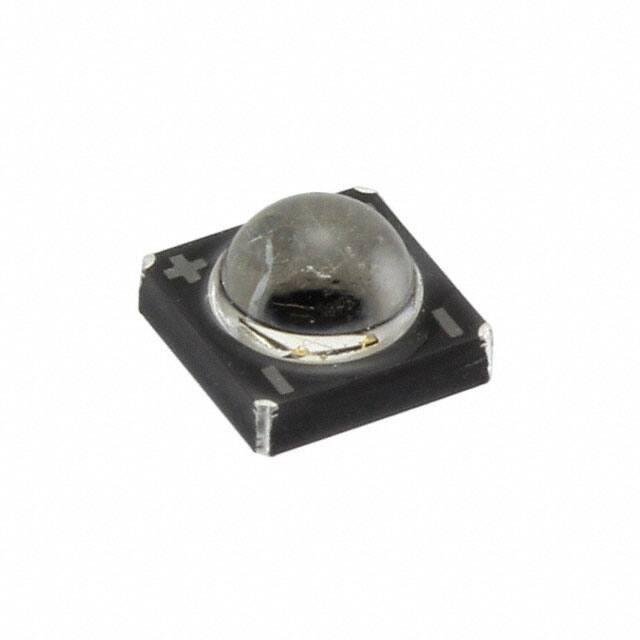
LED ENGIN LuxiGen
LZ1-00UBN0
Industry most robust high power ceramic package with glass
lens for high performance over life.
Applications
- Electronic Equipment
- Equipment Illumination (e.g. Curing, Endoscope)
- Gaming, Amusement, Gambling
- Horticulture Lighting
Features
- Package: Ceramic package with integrated glass lens
- Chip technology: UX:3
- Typ. Radiation: 60°
- Color: λpeak = 395 nm (● violet)
2 | Version 1.0 | 2022-06-25
- Industrial Automation (Machine Controls, Light
Barriers, Vision Controls)
- Photo Therapy
- Smoke/Dust/Particle Sensing
- Stage Lighting (LED & Laser)
�L Z1- 0 0UBN 0
DATASHEET
Ordering Information
Type
Total radiant flux 1)
IF = 700 mA
ΦE
Ordering Code
LZ1-00UBN0-00U4
1100 ... 2000 mW
Q65113A4143
LZ1-00UBN0-00U5
1100 ... 2000 mW
Q65113A4142
LZ1-00UBN0-00U8
1100 ... 2000 mW
Q65113A4141
3 | Version 1.0 | 2022-06-25
�L Z1- 0 0UBN 0
DATASHEET
Maximum Ratings
Parameter
Symbol
Operating Temperature
Top
min.
max.
-30 °C
100 °C
Storage Temperature
Tstg
min.
max.
-40 °C
125 °C
Junction Temperature 2)
Tj
max.
115 °C
Forward Current 2)
IF
max.
700 mA
Forward Current pulsed
t ≤ 10 ms; D ≤ 0.1 ; TC = 25 °C
IF pulse
max.
700 mA
ESD withstand voltage
acc. ANSI/ESDA/JEDEC JS-001 (HBM, Class 0)
VESD
Reverse voltage 3)
VR
4 | Version 1.0 | 2022-06-25
Values
ESD sensitive device
Not designed for
reverse operation
�L Z1- 0 0UBN 0
DATASHEET
Characteristics
IF = 700 mA; TC = 25 °C
Parameter
Symbol
Total radiant flux 4)
ΦE
typ.
Peak Wavelength 5)
IF = 700 mA
λpeak
min.
typ.
max.
Viewing angle at 50% IV
2φ
typ.
Forward Voltage 6)4)
IF = 700 mA
VF
min.
typ.
max.
Reverse current 3)
IR
Electrical thermal resistance junction/case
RthJC elec.
5 | Version 1.0 | 2022-06-25
Values
1450 mW
385 nm
395 nm
410 nm
70 °
3.20 V
3.70 V
4.20 V
Not designed
for reverse
operation
typ.
2.0 K / W
�L Z1- 0 0UBN 0
DATASHEET
Brightness Groups
Group
Total radiant flux 1)
IF = 700 mA
min.
ΦE
Total radiant flux 1)
IF = 700 mA
max.
ΦE
M1
1100 mW
1375 mW
N1
1375 mW
1760 mW
P1
1760 mW
2000 mW
Wavelength Groups
Group
Peak Wavelength 5)
IF = 700 mA
min.
λpeak
Peak Wavelength 5)
IF = 700 mA
max.
λpeak
U4
385 nm
390 nm
U5
390 nm
395 nm
U8
405 nm
410 nm
Group Name on Label
Example: M1-U4
Brightness
Wavelength
M1
U4
6 | Version 1.0 | 2022-06-25
�L Z1- 0 0UBN 0
DATASHEET
Relative Spectral Emission
4)
Irel = f (λ); IF = 700 mA; TC = 25 °C
Irel
LZ1-00UBN0
1,0
: Vλ
: U8
: U5
: U4
0,8
0,6
0,4
0,2
0,0
350
400
Radiation Characteristics
450
500
550
600
650
700
750
800
λ / nm
4)
Irel = f (ϕ); TC = 25 °C
LZ1-00UBN0
ϕ/°
-40°
-50°
-20°
-10°
0° 10° 20° 30° 40° 50° 60° 70° 80° 90°
1,0
-30°
0,8
0,6
-60°
-70°
0,4
-80°
0,2
-90°
0,0
-100°
7 | Version 1.0 | 2022-06-25
Irel
�L Z1- 0 0UBN 0
DATASHEET
Forward current
Relative Radiant Power
4)
IF = f(VF); TC = 25 °C
IF / A
ΦE/ΦE(700 mA) = f(IF); TC = 25 °C
LZ1-00UBN0
Φe
LZ1-00UBN0
700
Φe(700A) 1,0
: U8
: U5
: U4
600
4), 7)
: U8
: U5
: U4
0,8
500
0,6
400
300
0,4
200
0,2
100
Peak Wavelength
4)
Δλpeak = λpeak - λpeak(25 °C) = f(Tj); IF = 700 mA
LZ1-00UBN0
∆λ peak / nm
: U8
: U5
: U4
6
4
2
0
-2
70
0
60
0
50
0
40
0
30
0
20
0
10
0
20
-4
IF / A
8 | Version 1.0 | 2022-06-25
70
0
60
0
50
0
3,8 4,0
VF / V
40
0
3,6
30
0
3,4
20
0
3,2
10
0
0,0
20
20
2,93,0
IF / A
�L Z1- 0 0UBN 0
DATASHEET
Forward Voltage
Relative Radiant Power
4)
ΔVF = VF - VF(25 °C) = f(Tj); IF = 700 mA
∆VF / V
ΦE/ΦE(25 °C) = f(Tj); IF = 700 mA
LZ1-00UBN0
0,20
Φe
: U8
: U5
: U4
0,15
4)
LZ1-00UBN0
1,2
Φe (25°C)
1,0
0,10
0,8
0,05
0,6
0,00
-0,05
0,4
-0,10
0,2
-0,15
-40 -20 0
Peak Wavelength
20 40 60 80 100 120
Tj / °C
4)
Δλpeak = λpeak - λpeak(25 °C) = f(Tj); IF = 700 mA
∆λ peak / nm
LZ1-00UBN0
10
8
: U8
: U5
: U4
6
4
2
0
-2
-4
-6
20 40 60 80 100 120
Tj / °C
-8
-40 -20 0
9 | Version 1.0 | 2022-06-25
: U8
: U5
: U4
0,0
-40 -20 0
20 40 60 80 100 120
Tj / °C
�L Z1- 0 0UBN 0
DATASHEET
Max. Permissible Forward Current
IF = f(T)
IF / mA
800
all chips on
LZ1-00UBN0
700
600
500
400
300
200
100
0
20
40
60
10 | Version 1.0 | 2022-06-25
80
100
TC / °C
�L Z1- 0 0UBN 0
DATASHEET
Dimensional Drawing
8)
Further Information:
93.9 mg
Approximate Weight:
11 | Version 1.0 | 2022-06-25
�L Z1- 0 0UBN 0
DATASHEET
Electrical Internal Circuit
12 | Version 1.0 | 2022-06-25
�L Z1- 0 0UBN 0
DATASHEET
Recommended Solder Pad
8)
1. For superior solder joint connectivity results we recommend soldering under standard nitrogen atmosphere.
2. Package not suitable for ultra sonic cleaning.
3. Pedestal MCPCB allows the emitter thermal slug to be soldered directly to the metal core of the MCPCB. Such MCPCB
eliminate the high thermal resistance dielectric layer that standard MCPCB technologies use in between the emitter thermal
slug and the metal core of the MCPCB, thus lowering the overall system thermal resistance.
4. X-ray sample monitoring for solder voids underneath the emitter thermal slug is recommended. The total area covered by
solder voids should be less than 20% of the total emitter thermal slug area. Excessive solder voids will increase the emitter to
MCPCB thermal resistance and may lead to higher failure rates due to thermal over stress.
13 | Version 1.0 | 2022-06-25
�L Z1- 0 0UBN 0
DATASHEET
Reflow Soldering Profile
Product complies to MSL Level 1 acc. to JEDEC J-STD-020E
OHA04525
300
˚C
T 250
Tp 245 ˚C
240 ˚C
tP
217 ˚C
200
tL
150
tS
100
50
25 ˚C
0
0
50
100
150
200
250
s 300
t
Profile Feature
Symbol
Pb-Free (SnAgCu) Assembly
Minimum
Recommendation
Ramp-up rate to preheat*)
25 °C to 150 °C
tS
Time tS
TSmin to TSmax
Ramp-up rate to peak*)
TSmax to TP
Liquidus temperature
60
Maximum
2
3
100
120
2
3
Unit
K/s
s
K/s
TL
217
Time above liquidus temperature
tL
80
100
s
Peak temperature
TP
245
250
°C
Time within 5 °C of the specified peak
temperature TP - 5 K
tP
20
30
3
4
Ramp-down rate*
TP to 100 °C
10
Time
25 °C to TP
All temperatures refer to the center of the package, measured on the top of the component
* slope calculation DT/Dt: Dt max. 5 s; fulfillment for the whole T-range
14 | Version 1.0 | 2022-06-25
°C
480
s
K/s
s
�L Z1- 0 0UBN 0
DATASHEET
Taping
8)
15 | Version 1.0 | 2022-06-25
�L Z1- 0 0UBN 0
DATASHEET
Tape and Reel
9)
Reel Dimensions
A
180 mm
W
Nmin
12 + 0.3 / - 0.1 mm
16 | Version 1.0 | 2022-06-25
W1
60 mm
W2 max
12.4 + 2 mm
18.4 mm
Pieces per PU
500
�L Z1- 0 0UBN 0
DATASHEET
Barcode-Product-Label (BPL)
2�
��������� �����������������
�����������������
������ ����������������
���������
��
�������������������
����������������
���#������������
3�
"(.$�./�������
� ���1 �
���������
",$�,
-��((((
��0����
� �2
��
�� �2�� �
"#�$���
�%����������#&'()
'()
"��$���
����������#&'()
"�$��*�+����������#&'
� ���� �����!����
))�
17 | Version 1.0 | 2022-06-25
�L Z1- 0 0UBN 0
DATASHEET
Notes
The evaluation of eye safety occurs according to the standard IEC 62471:2006 (photo biological safety of
lamps and lamp systems). Within the risk grouping system of this IEC standard, the device specified in this
data sheet fall into the class high risk (exposure time less then 0.25 s). Under real circumstances (for exposure time, conditions of the eye pupils, observation distance), it is assumed that no endangerment to the
eye exists from these devices. As a matter of principle, however, it should be mentioned that intense light
sources have a high secondary exposure potential due to their blinding effect. When looking at bright light
sources (e.g. headlights), temporary reduction in visual acuity and afterimages can occur, leading to irritation, annoyance, visual impairment, and even accidents, depending on the situation.
Subcomponents of this device contain, in addition to other substances, metal filled materials including silver.
Metal filled materials can be affected by environments that contain traces of aggressive substances. Therefore, we recommend that customers minimize device exposure to aggressive substances during storage,
production, and use. Devices that showed visible discoloration when tested using the described tests above
did show no performance deviations within failure limits during the stated test duration. Respective failure
limits are described in the IEC60810.
Tapes and reels are shipped in airtight bags in order to reduce the onset of silver tarnish. We recommend
bags only be opened when ready to use emitters. Partially used reels or trays should be stored in airtight
bags or in storage purged with nitrogen.
Based on very short life cycle times in chip technology this component is subject to frequent adaption to the
latest chip technology.
Changes to the content of this datasheet may occur without further notification. JEDEC 46C constitutes the
guideline of the change management for the device specified in this document.
For further application related information please visit www.osram-os.com/appnotes
18 | Version 1.0 | 2022-06-25
�L Z1- 0 0UBN 0
DATASHEET
Disclaimer
Attention please!
The information describes the type of component and shall not be considered as assured characteristics.
Terms of delivery and rights to change design reserved. Due to technical requirements components may
contain dangerous substances.
For information on the types in question please contact our Sales Organization.
If printed or downloaded, please find the latest version on our website.
Packing
Please use the recycling operators known to you. We can also help you – get in touch with your nearest
sales office. By agreement we will take packing material back, if it is sorted. You must bear the costs of
transport. For packing material that is returned to us unsorted or which we are not obliged to accept, we
shall have to invoice you for any costs incurred.
Product and functional safety devices/applications or medical devices/applications
Our components are not developed, constructed or tested for the application as safety relevant component
or for the application in medical devices.
Our products are not qualified at module and system level for such application.
In case buyer – or customer supplied by buyer – considers using our components in product safety devices/
applications or medical devices/applications, buyer and/or customer has to inform our local sales partner
immediately and we and buyer and /or customer will analyze and coordinate the customer-specific request
between us and buyer and/or customer.
19 | Version 1.0 | 2022-06-25
�L Z1- 0 0UBN 0
DATASHEET
Glossary
1)
Brightness: Brightness groups are tested at a current pulse duration of 10 ms and a tolerance of
±10 %.
2)
Operating Conditions: Operating conditions according DC-derating (Max. Permissible Forward Current)
3)
Reverse Operation: Not designed for reverse operation. Continuous reverse operation can cause migration and damage of the device.
4)
Typical Values: Due to the special conditions of the manufacturing processes of semiconductor devices, the typical data or calculated correlations of technical parameters can only reflect statistical figures.
These do not necessarily correspond to the actual parameters of each single product, which could differ from the typical data and calculated correlations or the typical characteristic line. If requested, e.g.
because of technical improvements, these typ. data will be changed without any further notice.
5)
Peak Wavelength: Wavelengths are tested at a current pulse duration of 10 ms and a tolerance of
±2 nm.
6)
Forward Voltage: Forward voltages are tested at a current pulse duration of 10 ms and a tolerance of
±0.1 V.
7)
Characteristic curve: In the range where the line of the graph is broken, you must expect higher differences between single devices within one packing unit.
8)
Tolerance of Measure: Unless otherwise noted in drawing, tolerances are specified with ±0.1 and
dimensions are specified in mm.
9)
Tape and Reel: All dimensions and tolerances are specified acc. IEC 60286-3 and specified in mm.
20 | Version 1.0 | 2022-06-25
�L Z1- 0 0UBN 0
DATASHEET
Revision History
Version
Date
Change
1.0
2022-06-25
Electro - Optical Characteristics (Diagrams)
New Layout
Derating (Diagrams)
Maximum Ratings
21 | Version 1.0 | 2022-06-25
�L Z1- 0 0UBN 0
DATASHEET
Published by ams-OSRAM AG
Tobelbader Strasse 30, 8141 Premstaetten, Austria
Phone +43 3136 500-0
ams-osram.com
© All rights reserved
22 | Version 1.0 | 2022-06-25
�


 工商网监
湘ICP备2023018690号
工商网监
湘ICP备2023018690号
