SLG5NT1581V
7.3 mΩ, 9 A GreenFET 3
Load Switch with Discharge
General Description
Pin Configuration
The SLG5NT1581V is designed for load switching application.
The part comes with one 9 A rated MOSFET switched on by
an ON control pin. MOSFET turn on time is independently adjusted by an external capacitor.
MOS_D
1
14
MOS_D
2
13
MOS_S
MOS_S
ON_MOS
3
12
CAP_MOS
VDD
4
11
GND
ON_MOS
5
10
CAP_MOS
MOS_D
6
9
MOS_D
7
8
MOS_S
MOS_S
Features
•
•
•
•
•
•
•
•
One 9 A independent MOSFET
Integrated VGS Charge Pump
Internal discharge for gate and source
User selectable ramp control by external capacitor
Protected by thermal shutdown with current limit
Pb-Free / RoHS Compliant
Halogen-Free
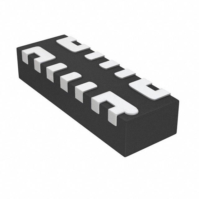
STDFN 14L, 1 x 3 x 0.55 mm
14-pin STDFN
(Top View)
Target Applications
• Consumer Electronics
• Portable: Tablets, Notebooks
• PCs and PC peripherals
• Commercial and Industrial Electronics
• Printers
• Servers
• Embedded PCs
• Data Communications Equipment
Block Diagram
9 A @ 7.3 mΩ
MOS_D
+2.7 to 5.5 V
CAP
MOS_S
Charge
Pump
PIN10
Linear Ramp
Control
PIN12
Over Current and
Over Temperature
Protection
PIN3
ON/OFF
CMOS Input
PIN5
Silego Technology, Inc.
000-005NT1581-102
Rev 1.02
Revised June 18, 2014
�SLG5NT1581V
Pin Description
Pin #
Pin Name
Type
Pin Description
1
MOS_D
MOSFET
Drain of MOSFET
2
MOS_D
MOSFET
Drain of MOSFET
3
ON_MOS
Input
Turns on MOS (4 MΩ pull down resistor). Tied to Pin 5 on PCB.
4
VDD
VDD
+5VDD Power
5
ON_MOS
Input
Turns on MOS (4 MΩ pull down resistor). Tied to Pin 3 on PCB.
6
MOS_D
MOSFET
Drain of MOSFET
7
MOS_D
MOSFET
Drain of MOSFET
8
MOS_S
MOSFET
Source of MOSFET
9
MOS_S
MOSFET
Source of MOSFET
10
CAP_MOS
Input
Sets ramp and turn on time for MOSFET. Tied to Pin 12 on PCB.
11
GND
GND
Ground
12
CAP_MOS
Input
Sets ramp and turn on time for MOSFET. Tied to Pin 10 on PCB.
13
MOS_S
MOSFET
Source of MOSFET
14
MOS_S
MOSFET
Source of MOSFET
Ordering Information
Part Number
Type
Production Flow
SLG5NT1581V
STDFN 14L
Industrial, -40 °C to 85 °C
SLG5NT1581VTR
STDFN 14L (Tape and Reel)
Industrial, -40 °C to 85 °C
000-005NT1581-102
Page 2 of 9
�SLG5NT1581V
Absolute Maximum Ratings
Parameter
Description
VD
Power Supply
TS
Storage Temperature
ESDHBM
WDIS
IDSMAX
ESD Protection
Conditions
Human Body Model
Min.
Typ.
Max.
Unit
--
--
6
V
-65
--
150
°C
2000
--
--
V
--
--
1.2
W
9
A
12
A
Package Power Dissipation
Max Operating Current
MOSFET IDSPK Peak Current from Drain to Source
For no more than 10 continuous seconds
out of every 100 seconds
--
--
Note: Stresses greater than those listed under “Absolute Maximum Ratings” may cause permanent damage to the device. This is a stress rating
only and functional operation of the device at these or any other conditions above those indicated in the operational sections of this
specification is not implied. Exposure to absolute maximum rating conditions for extended periods may affect reliability.
Electrical Characteristics
TA = -40 °C to 85 °C (unless otherwise stated)
Parameter
VDD
IDD
RDSON
Description
Conditions
Power Supply Voltage
Min.
VD
TON_Delay
--
5.5
V
--
0.1
1
μA
Power Supply Current
ON_MOS_1 & ON_MOS_2
(Steady State)
--
50
75
μA
TA 25°C MOSFET @100 mA
--
7.3
9
mΩ
TA 70°C MOSFET @100 mA
--
8.5
11
mΩ
8
11.5
mΩ
--
9
A
1.0
5.0
VDD
V
0
300
500
μs
ON Resistance
Current from Drain to Source for
each MOSFET
Continuous
Drain Voltage
ON pin Delay Time
50% ON to Ramp Begin
--
Configurable 1
Total Turn On Time
Example: CAP (Pin 10 & 12) share
a single 4nF capacitor, VDD = VD = 5
V, Source_Cap = 10 μF, RL = 20 Ω
--
Slew Rate
Example: CAP (Pin 10 & 12) share
a single 4nF capacitor, VDD = VD = 5
V, Source_Cap = 10 μF, RL = 20 Ω
1.1
ms
--
Configurable 1
10% VS to 90% VS
TSLEWRATE
Unit
2.5
50% ON to 90% VS
TTotal_ON
Max.
Power Supply Current when OFF
TA 85°C MOSFET @100 mA
MOSFET
IDS
Typ.
--
ms
V/ms
6.0
--
V/ms
--
--
1000
μF
Discharge Resistance
100
210
300
Ω
ON_VIH
High Input Voltage on ON pin
0.85
--
VDD
V
ON_VIL
Low Input Voltage on ON pin
-0.3
0
0.3
V
CAPSOURCE Source Cap
RDIS
Source to GND
Active Current Limit
MOSFET will automatically limit current when VS > 250 mV
--
12.0
--
A
Short Circuit Current Limit
MOSFET will automatically limit current when VS < 250 mV
--
0.5
--
A
Thermal shutoff turn-on temperature
--
125
--
°C
THERMOFF Thermal shutoff turn-off temperature
--
100
--
°C
ILIMIT
THERMON
000-005NT1581-102
Page 3 of 9
�SLG5NT1581V
TA = -40 °C to 85 °C (unless otherwise stated)
Parameter
Description
Conditions
THERMTIME Thermal shutoff time
TOFF_Delay
OFF Delay Time
50% ON to VS Fall, VDD = VD = 5 V
Min.
Typ.
Max.
Unit
--
--
1
ms
--
--
15
μs
Notes:
1. Refer to table for configuration details.
000-005NT1581-102
Page 4 of 9
�SLG5NT1581V
TSLEW vs. CAP
Slew Rate (V/ms) Vs. Cap, VDD = 5V, TA = 25C
10%VS to 90%VS, RL = 20 ohm, CL = 10 uF
30.000
25.000
20.000
V/ms
VD = 1.5V
15.000
VD = 2.5V
10.000
VD = 3.3V
VD = 5V
5.000
0.000
0
2
4
6
8
10
12
14
16
18
20
22
24
26
Cap (nF)
TTOTAL_ON vs. CAP
Ttotal_on vs Cap. 50%ON to 90%VS, TA = 25C
VDD = 5V, RL = 20 ohm, CL = 10 uF
6.000
Ttotal_on (ms)
5.000
4.000
VD = 1.5V
3.000
VD = 2.5V
2.000
VD = 3.3V
VD = 5V
1.000
0.000
0
2
4
6
8
10
12
14
16
18
20
22
24
26
Cap (nF)
000-005NT1581-102
Page 5 of 9
�SLG5NT1581V
TTotal_ON, TON_Delay and Slew Rate Measurement
ON
50% ON
50% ON
TOFF_DELAY
90% VS
VS
90% VS
TON_DELAY
10% VS
10% VS
Slew Rate (V/ms)
TFALL
TTotal_ON
000-005NT1581-102
Page 6 of 9
�SLG5NT1581V
Package Top Marking System Definition
Part Code
PPDDL
Lot #
Pin 1 Identifier
Date Code
000-005NT1581-102
Page 7 of 9
�SLG5NT1581V
Package Drawing and Dimensions
14 Lead STDFN Package 1 mm x 3 mm (Fused Lead)
000-005NT1581-102
Page 8 of 9
�SLG5NT1581V
Tape and Reel Specifications
Package
Type
# of
Pins
Nominal
Package
Size
14STDFN
14
1x3x0.55mm
Trailer A
Leader B
Pocket Tape(mm)
Max
Reel &
Units per
Units Hub Size
Length Width
Reel
Pockets Length
Pitch
per Box
(mm)
(mm) Pockets (mm)
3000
3000
178/60
42
168
42
168
8
4
Tape and Reel Drawing
Symbol
Ao
Bo
Ko
Po
P1
W
000-005NT1581-102
Dimension (mm)
2.25 ± 0.10
3.30 ± 0.10
1.20 ± 0.10
4.0 ± 0.10
4.0 ± 0.10
8.0 ± 0.20
Symbol
P2
Do
D1
E
F
T
Dimension (mm)
2.0 ± 0.05
1.55 ± 0.05
1.10 ± 0.10
1.75 ± 0.10
3.50 ± 0.05
0.25 ± 0.05
Page 9 of 9
�
很抱歉,暂时无法提供与“SLG5NT1581VTR”相匹配的价格&库存,您可以联系我们找货
免费人工找货