UMW
■
R
SN74LVC1G00
Product introduction
SN74LVC1G00 is a 2-input NAND integrated circuit, which can realize the mathematical logic operation of
and
. Advanced CMOS process design is adopted, which has the working characteristics of low power
consumption and high output driving capability. The chip can work normally when the power supply voltage VCC is
between 1.65V and 5.5V V. And 74LVC1G00 has a variety of small package shapes,It can be widely used in high-end
precision instruments, miniaturized low-power handheld devices, artificial intelligence and other fields.
■
Product features
●
●
●
■
Low static power consumption: 0.1uA typical ●
Wide working voltage range: 1.65V to 5.5V
Package form: DBV/DCK/DRL/YZP/ DRY/DSF/ DPW
High output drive: VCC=4.5V, more than 32MA
product usage
●
●
●
■
●
Low input current: 0.1uA typical
Portable audio interface
● Blu-ray player and home theater
digital television
● Solid state drive
Wireless headphones, smart watches, etc.
● Smart wearable devices
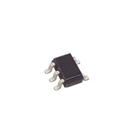
Package form and pin function definition
SOT23-5
SC70-5
SOT-553
SOT-886
SON-6
DSBGA-5
X2SON-5
Pin
Name
DBV/ DCK/ DRL
DRY/DSF
YZP
DPW
Description
NC
1
1,5
A1, B2
1
Empty foot
A
2
2
B1
2
Input
GND
3
3
C1
3
Y
4
4
C2
4
VCC
5
6
A2
5
Power supply ground
Output
Power supply positive
Note: NC null pin, no connecting wire inside.
www.umw-ic.com
1
UTD Semiconductor Co.,Limited
semiconductor co.,
ltd
�UMW
■
R
SN74LVC1G00
Limit parameter
parameter
symbol
limit
value
6.5
unit
operating voltage
VCC
input
VIN
-0.5~6.5
V
Output voltage (1)
VOUT
-0.5~6.5
V
Single pin output
current
Or Vcc current.
IOUT
25
mA
ICC
50
mA
Storage temperature
TS
-65-150
℃
Pin welding
temperature
TW
260,10s
℃
V
Note: 1. In the power-off state of VCC=0V, the limit voltage that the output can bear,
2. Limit parameter refers to the limit value that can't be exceeded under any conditions. If it exceeds this limit value, it may cause
physical damage such as product deterioration; At the same time, the chip can't work normally when it is close to the limit parameters.
■
Principle logic diagram
■ truth table
Inputs
A
B
L
L
L
H
H
L
H
H
■
Output
Y
H
H
H
L
working conditions
project
operating
voltage
symbol
VC
test condition
minimum
value
1.65
typical
value
-
0.65* VC
-
-
1.7V
-
-
VC =3V~5.5V
0.7* VC
-
-
VC =1.65V~1.95V
-
-
VC =2.3V~2.7V
-
-
0.7
VC =3V~5.5V
-
-
0.3* VC
VC =1.65V~1.95V
Input high level
voltage
Input high level
voltage
input
voltage
Output
voltage
High level output
current
Low level output
current
www.umw-ic.com
VHI
VHI
VC =2.3V~2.7V
maximum
5.5
unit
V
V
0.35* VC
V
VI
-
0
-
5.5
V
VO
-
0
-
VC
V
VC =1.65V
-
-
-4
VC =2.3V
-
-
-8
VC =3V
-
-
-16
VC =4.5V
-
-
-32
VC =1.65V
-
-
4
VC =2.3V
-
-
8
VC =3V
-
-
16
VC =4.5V
-
-
32
IOH
IOL
2
mA
mA
UTD Semiconductor Co.,Limited
semiconductor co.,
ltd
�UMW
■
R
SN74LVC1G00
Electrical characteristics
Electrical characteristics of DC: T =25℃
A
project
symbol
High level load
voltage
VOH
Low level load
voltage
incoming current
Turn-off current
operational
current
Working current
variation value
Ac electrical characteristics:
project
VOL
A
II
B
IOFF
V
test condition
typical
value
maximum
IOH =-100uA
1.65V~5.5V
1.64
-
IOH =-4 mA
1.65V
1.47
-
IOH =-8 mA
2.3V
2.15
-
IOH =-16 mA
3V
2.73
-
IOH =-32 mA
4.5V
4.0
IOH =100uA
1.65V~5.5V
0.01
-
IOH =4 mA
1.65V
0.11
-
IOH =8 mA
2.3V
0.11
-
IOH =16 mA
3V
0.2
-
IOH =32 mA
4.5V
0.35
-
0~5.5V
0.01
±5
0.01
±5
VI =5.5V 或 GND
unit
V
V
uA
VI
VI =5.5V
0
0.01
±10
VO
VO =5.5V
0
0.01
±10
0.01
10
0.01
10
25
-
uA
25
-
uA
ICC
ICC
VI =5.5V,IO =0
1.65V~5.5V
VI =GND ,IO =0
A=VCC -0.6V
B=VCC 或 GND
uA
uA
3V~5.5V
B=VCC -0.6V
A= VCC 或 GND
Ta=25℃ V(298)=5.0V,tr =≤20ns. See test method.
symbol
Maximum transmission
delay time a, B
test
condition
minimum
value
typical
value
maximum
unit
C =15pF
-
10
-
ns
C =15pF
-
10
-
ns
to Y
Note: 1. CL capacitor is external chip capacitor (0603), which is connected close to the output pin,
and the capacitor ground is close to the chip GND;
2. Input: port input level, f=500kHz,D=50%; tr=tf≤20ns;
3. Output: Y-terminal output test.
www.umw-ic.com
3
UTD Semiconductor Co.,Limited
semiconductor co.,
ltd
�UMW
R
SN74LVC1G00
■ Encapsulated information
DBV(SOT23-5)
■ Marking
C00K
www.umw-ic.com
4
UTD Semiconductor Co.,Limited
semiconductor co.,
ltd
�UMW
R
SN74LVC1G00
DCK(SC70-5)
■ Marking
www.umw-ic.com
5
UTD Semiconductor Co.,Limited
semiconductor co.,
ltd
�UMW
R
SN74LVC1G00
DRL(SOT-553)
www.umw-ic.com
6
UTD Semiconductor Co.,Limited
semiconductor co.,
ltd
�UMW
R
SN74LVC1G00
DRY(SOT-886)
www.umw-ic.com
7
UTD Semiconductor Co.,Limited
semiconductor co.,
ltd
�UMW
R
SN74LVC1G00
DSF(SON-6)
www.umw-ic.com
8
UTD Semiconductor Co.,Limited
semiconductor co.,
ltd
�UMW
R
SN74LVC1G00
YZP(DSBGA-5)
www.umw-ic.com
9
UTD Semiconductor Co.,Limited
semiconductor co.,
ltd
�UMW
R
SN74LVC1G00
DPW(X2SON-4)
www.umw-ic.com
10
UTD Semiconductor Co.,Limited
semiconductor co.,
ltd
�
很抱歉,暂时无法提供与“SN74LVC1G00DCKR”相匹配的价格&库存,您可以联系我们找货
免费人工找货