US Headquarters
2950 Red Hill Ave, Costa Mesa
California, USA 92626
Office: 714.913.2200
Fax: 714.913.2202
www.vikingtechnology.com
Datasheet for:
SDHC/SDXC UHS104
microSD Cards
PSFUSDxxxxCxxxxx_W
microSD Cards
�Legal Information
Copyright© 2020 Sanmina Corporation. All rights reserved. The information in this document is
proprietary and confidential to Sanmina Corporation. No part of this document may be
reproduced in any form or by any means or used to make any derivative work (such as
translation, transformation, or adaptation) without written permission from Sanmina. Sanmina
reserves the right to revise this documentation and to make changes in content from time to
time without obligation on the part of Sanmina to provide notification of such revision or change.
Sanmina provides this documentation without warranty, term or condition of any kind, either
expressed or implied, including, but not limited to, expressed and implied warranties of
merchantability, fitness for a particular purpose, and non-infringement. While the information
contained herein is believed to be accurate, such information is preliminary, and should not be
relied upon for accuracy or completeness, and no representations or warranties of accuracy or
completeness are made. In no event will Sanmina be liable for damages arising directly or
indirectly from any use of or reliance upon the information contained in this document. Sanmina
may make improvements or changes in the product(s) and/or the program(s) described in this
documentation at any time.
Sanmina, Viking Technology, Viking Modular Solutions, and the Viking logo are trademarks of
Sanmina Corporation. Other company, product or service names mentioned herein may be
trademarks or service marks of their respective owners.
Datasheet: PSFUSDxxxxCxxxxx_W
Revision F | January 21, 2020
SDHC/SDXC UHS104 microSD Cards
Page 2
�Revision History
Date
Revisio
n
4/15/19
A
10/2/19
B
10/14/19
C
11/1/19
D
11/15/19
E
1/21/20
F
Description
Revised from PSUSDxxxxCxxxxxC_A
Remove references to tos, change
performance. Change to TLC
Add new PN’s per PSG 9/25/19. Add
VWFUSD016GCEDWW PN per agile
Add VWFUSD016GCEDWW PN per agile
Add specs for 256GB
Revise VWFUSD8192CEWWW to
(-25to+85ºC)
Add VWUSD128GCEHWW3C
VWUSD064GCE5WW3C
Datasheet: PSFUSDxxxxCxxxxx_W
Revision F | January 21, 2020
Checked by
SDHC/SDXC UHS104 microSD Cards
Page 3
�Ordering Information for the SDHC/SDXC UHS104 microSD Cards
VikingPart#
Interface
Temp
GB
Client/Ent
NAND
VWFUSD8192CEWWW
VWFUSD016GCEDWW
VWUSD032GCE1WW3C
VWUSD064GCE5WW3C
VWUSD128GCEHWW3C
VWFUSD064GCEAMWL
VWFUSD128GCEZMWL
VWFUSD256GCECMWL
microSD Card
microSD Card
microSD Card
microSD Card
microSD Card
microSD Card
microSD Card
microSD Card
(-25 to +85ºC)
(-25 to +85ºC)
(-25 to +85ºC)
(-25 to +85ºC)
(-25 to +85ºC)
(-25 to +85ºC)
(-25 to +85ºC)
(-25 to +85ºC)
8
16
32
64
128
64
128
256
Client
Client
Client
Client
Client
Client
Client
Client
TSB BiCS 3D
TSB BiCS 3D
TSB BiCS 3D TLC
TSB BiCS 3D TLC
TSB BiCS 3D TLC
SanDisk MLC
SanDisk MLC
SanDisk MLC
Notes:
1. Contact Viking for availability date
2. The lowercase letters x,y and z are wildcard characters that indicate product or customer specific information
3. Refer to the Viking part number coversheet or PN decoder for details.
Datasheet: PSFUSDxxxxCxxxxx_W
Revision F | January 21, 2020
SDHC/SDXC UHS104 microSD Cards
Page 4
�Table of Contents
1
INTRODUCTION
8
1.1
FEATURES
8
2
MICROSD CARD STANDARDS COMPATIBILITY
9
3
PHYSICAL CHARACTERISTICS
9
3.1
Package Characteristics
9
3.2
Environmental Characteristics
9
3.3
Physical Characteristics
10
4
ELECTRICAL INTERFACE
10
4.1
Pin Assignment
10
4.2
microSD Card Bus Topology
4.2.1
SD Bus Mode protocol
11
11
4.3
17
Initialization
4.4
Electrical Characteristics
4.4.1
Absolute Maximum Conditions
4.4.2
DC Characteristics
4.4.3
AC Characteristics (Default Speed)
4.4.4
AC Characteristics (High Speed)
4.4.5
AC Characteristics (Ultra High Speed; UHS104)
21
21
22
25
27
28
5
CARD INTERNAL INFORMATION
33
5.1
Security Information
33
5.2
microSD Card Registers
5.2.1
OCR Register
5.2.2
CID Register
5.2.3
CSD Register
5.2.4
RCA Register
5.2.5
DSR Register
5.2.6
SCR Register
5.2.7
Card Status
5.2.8
SD Status
5.2.9
Switch Function Status
33
34
35
35
37
37
37
38
40
41
5.3
Logical Format
5.3.1
microSD card Capacities
42
43
Datasheet: PSFUSDxxxxCxxxxx_W
Revision F | January 21, 2020
SDHC/SDXC UHS104 microSD Cards
Page 5
�6
SD SPECIFICATION COMPLIANCE
43
7
RELIABILITY GUIDANCE
43
8
MICROSD CARD MECHANICAL DIMENSIONS
45
Datasheet: PSFUSDxxxxCxxxxx_W
Revision F | January 21, 2020
SDHC/SDXC UHS104 microSD Cards
Page 6
�Table of Tables
Table 1-1: Features ___________________________________________________________________ 8
Table 4-1: microSD Card Pin Assignment ________________________________________________ 10
Table 4-2: SD Mode Command Set ( + = Implemented, - = Not Implemented) __________________ 12
Table 4-3: SPI Mode Command Set ( + = Implemented, - = Not Implemented) _________________ 15
Table 4-4:S18R and S18A Combinations _________________________________________________ 19
Table 4-5: Absolute Maximum Conditions ________________________________________________ 21
Table 4-6: DC Characteristics __________________________________________________________ 22
Table 4-7: Bus Operating Conditions - Signal Line's Load ____________________________________ 24
Table 4-8: Threshold Level 1.8V Signaling ________________________________________________ 24
Table 4-9: Threshold Level 1.8V Signaling ________________________________________________ 25
Table 4-10: Bus Timing - Parameters Values (Default Speed) _________________________________ 26
Table 4-11: Bus Timing - Parameters Values (High Speed) ___________________________________ 27
Table 4-12: Clock Signal Timing of SDR104, SDR50, SDR25, SDR12 __________________________ 29
Table 4-13: Clock input Timing of SDR104, SDR50, SDR25, SDR12 ___________________________ 29
Table 4-14: Output Timing of Fixed Data Window ( SDR50, SDR25, SDR12 ) ____________________ 30
Table 4-15: Output Timing of Variable Data Window ( SDR104 ) ______________________________ 31
Table 4-16: Clock Signal Timing of DDR50 _______________________________________________ 31
Table 4-17: BUS Timings – Parameters Values (DDR50 mode) _______________________________ 32
Table 5-1: microSD Card Registers _____________________________________________________ 34
Table 5-2: OCR register definition ______________________________________________________ 34
Table 5-3: CID register _______________________________________________________________ 35
Table 5-4: CSD register ______________________________________________________________ 35
Table 5-5: The SCR Fields ____________________________________________________________ 37
Table 5-6: Card Status _______________________________________________________________ 38
Table 5-7: SD Status _________________________________________________________________ 40
Table 5-8: Switch Function Status ______________________________________________________ 41
Table of Figures
Figure 1-1: Top View __________________________________________________________________ 9
Figure 4-1: microSD Card Pin Assignment (Back view of the Card) ____________________________ 10
Figure 4-2: Bus Connection Diagram (SD Mode) ___________________________________________ 12
Figure 4-3: Bus Connection Diagram (SPI Mode) __________________________________________ 15
Figure 4-4: UHS-I Host Initialization Flow Chart ____________________________________________ 17
Figure 4-5: ACMD41 Timing Followed by Signal Voltage Switch Sequence ______________________ 18
Figure 4-6: Signal Voltage Switch Sequence ______________________________________________ 20
Figure 4-7: microSD Card Connection Diagram ____________________________________________ 21
Figure 4-8: Card Input Timing (Default Speed Mode) ________________________________________ 25
Figure 4-9: Card Output Timing (Default Speed Mode) ______________________________________ 26
Figure 4-10: Card Input Timing (High Speed Card) _________________________________________ 27
Figure 4-11: Card Output Timing (High Speed Card) ________________________________________ 27
Figure 4-12: Clock Signal Timing _______________________________________________________ 28
Figure 4-13: Clock Input Timing ________________________________________________________ 29
Figure 4-14: Output Timing of Fixed Window ______________________________________________ 30
Figure 4-15: Output Timing of Variable Window ____________________________________________ 30
Figure 4-16: Clock Signal Timing _______________________________________________________ 31
Figure 4-17: Timing Diagram DAT Inputs/Outputs Referenced to CLK in DDR50 Mode _____________ 32
Datasheet: PSFUSDxxxxCxxxxx_W
Revision F | January 21, 2020
SDHC/SDXC UHS104 microSD Cards
Page 7
�1 Introduction
This data sheet describes the specifications of the SDHC/SDXC Standard microSD Card with
UHS104 SD Bus mode. The SDHC/SDXC microSD Cards are a Memory Card of Small and
Thin with SDMI compliant Security method. (SDMI: Secure Digital Music Initiative) Contents in
the Card can be protected by CPRM based security. This contents security can be
accomplished by SDHC/SDXC Card, host, and security application software combinations.
1.1 FEATURES
Table 1-1: Features
Media Format
microSD Memory Card
Standard
Compliant with the SD Memory Card Standard Ver. 4.20, UHS104
Security Functions
SD Security Specification Ver.2.00 Compliant (CPRM Based)
*CPRM: Contents Protection for Recording Media Specification
Logical Format
Electrical Features
Operating Voltage
Operating Current
SD Interface
UHS-I Interface
Physical Features
Physical Package size
/Mass
Durability
RoHS
Performance Features
Maximum access speed
Speed Class
Datasheet: PSFUSDxxxxCxxxxx_W
Revision F | January 21, 2020
SD File System Specification Ver.2.00 Compliant SDHC Card =
FAT32, SDXC Card = exFAT
VDD = 2.7V(min), 3.3V(Typ), 3.6V(max)
SDR104 Write : 140mA(max) SDR104 Read : 150mA(max)
DS : Signaling Voltage = 3.3V(Typ), SDCLK = 25MHz HS :
Signaling Voltage = 3.3V(Typ), SDCLK = 50MHz
Ultra High Speed:
UHS104 : Signaling Voltage = 1.8V(Typ), SDCLK = 208MHz
UHS50 : Signaling Voltage = 1.8V(Typ), SDCLK =
100MHz@SDR100 / 50MHz@DDR50 Supported UHS-I bus
modes are SDR104, SDR50, DDR50, SDR25, SDR12.
L: 15, W: 11, T: 1 (mm), Weight: 0.3g (typ.) SD Physical Layer
Specification Ver.3.01 Compliant
Compliant with SD Physical Layer Specification Ver.3.01 and
microSD Memory Card specification 2.01 Compliant
Compliant with RoHS regulations (DIRECTIVE 2011/65/EU)
Bus mode Sequential Write = 50 MB/s Sequential Read = 80 MB/s
UHS Speed Class = U3 SD Speed Class = C10, Class 4
SDHC/SDXC UHS104 microSD Cards
Page 8
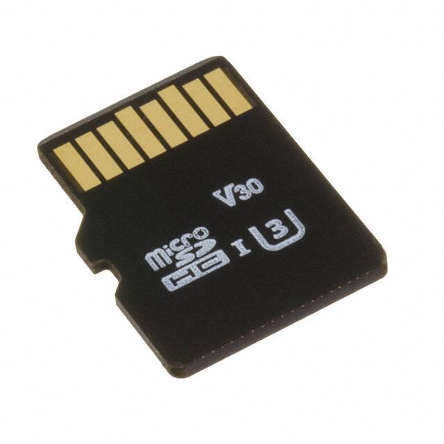
�Figure 1-1: Top View
2 microSD Card Standards Compatibility
This microSD Memory Card Specification is compliant with:
PHYSICAL LAYER SPECIFICATION Ver.3.01 (Part1)
(Except for Mechanical Specification)
FILE SYSTEM SPECIFICATION Ver.2.00. (Part2)
SECURITY SPECIFICATION Ver.2.00. (Part3)
microSD Card Memory Card Specification Version 2.01
3 Physical Characteristics
3.1
Package Characteristics
1. Mold Material: Epoxy Resin+Silicon Dioxide
2. Flameproof Grade: V-0(UL94)
3. Heatproof Temperature: approx.400 degrees
3.2 Environmental Characteristics
The standard Operation Conditions are:
Absolute Maximum Temperature Range
Humidity less than RH = 95 %, Non condensed
Ta = -25 to +85°C
Ta = 25°C
The standard Storage Conditions are:
Maximum Temperature Range:
Humidity less than RH = 93%, Non condensed
Tstg = -40 to +85°C
Ta = 40°C
Datasheet: PSFUSDxxxxCxxxxx_W
Revision F | January 21, 2020
SDHC/SDXC UHS104 microSD Cards
Page 9
�3.3 Physical Characteristics
1) Hot Insertion or Removal
The microSD Card can be removed or inserted without power off from the host system as
described in the SD Physical Layer Specification 6.1
The connector will recognize the Hot Insertion or Removal is defined in the 6.2 of the PHYSICAL
LAYER SPECIFICATION.
2) Mechanical Write Protect Switch
The microSD memory Card has no mechanical write protect switch.
4 Electrical Interface
4.1 Pin Assignment
The table below describes the pin assignment of the microSD card. The following
figure describes the pin assignment of the microSD card. Please refer to the detail
descriptions by SD Card Physical Layer Specification.
Figure 4-1: microSD Card Pin Assignment (Back view of the Card)
Table 4-1: microSD Card Pin Assignment
SD Mode
SPI Mode
Pin
Name
IO Type
Description
Name
IO Type
Description
1
DAT2
I/O/PP
Data Line[Bit2]
RSV
I/O/ PP
Card Detect/ Data Line[Bit3]
CS
I
PP
Command/Response
DI
I
Chip Select
(Negative True)
Data In
S
Supply Voltage
VDD
S
Supply Voltage
3
CD/
DAT3
CMD
4
VDD
5
CLK
I
Clock
SCLK
I
Clock
6
VSS
S
Ground
VSS
S
Ground
7
DAT0
I/O/PP
Data Line[Bit0]
DO
O/PP
Data Out
8
DAT1
I/O/PP
Data Line[Bit1]
RSV
-
Reserved(*)
2
Datasheet: PSFUSDxxxxCxxxxx_W
Revision F | January 21, 2020
SDHC/SDXC UHS104 microSD Cards
Page 10
�Notes:
S: Power Supply
I: Input
O: Output using push-pull drivers
PP: I/O using push-pull drivers
(*) These signals should be pulled up by host side with 10-100k ohm resistance in the SPI Mode.
4.2 microSD Card Bus Topology
The device supports two alternative communication protocols: SD and SPI Bus Mode. It is as
same as standard microSD memory cards. Host System can choose either one of modes.
Same Data of the device can read and write by both modes. SD Mode allows the 4-bit high
performance data transfer. SPI Mode allows easy and common interface for SPI channel. The
disadvantage of this mode is loss of performance, relatively to the SD mode.
4.2.1 SD Bus Mode protocol
The SD bus allows the dynamic configuration of the number of data line from 1 to 4 Bidirectional data signal. After power up by default, the Device will use only DAT0. After
initialization, host can change the bus width. Multiplied microSD cards connections are available
to the host. Common VDD, VSS and CLK signal connections are available in the multiple
connections. However, Command, Respond and Data lined (DAT0-DAT3) shall be divided for
each card from host. This feature allows easy tradeoff between hardware cost and system
performance. Communication over the SD bus is based on command and data bit stream
initiated by a start bit and terminated by stop bit.
Command:
Commands are transferred serially on the CMD line. A command is a token to starts an
operation from host to the card. Commands are sent to an addressed single card (addressed
Command) or to all connected cards (Broad cast command).
Response:
Responses are transferred serially on the CMD line. A response is a token to answer to a
previous received command. Responses are sent from an addressed single card or from all
connected cards.
Data:
Data can be transfer from the card to the host or vice versa. Data is transferred via the data
lines.
Datasheet: PSFUSDxxxxCxxxxx_W
Revision F | January 21, 2020
SDHC/SDXC UHS104 microSD Cards
Page 11
�microSD Card
(A)
microSD Card
(B)
Figure 4-2: Bus Connection Diagram (SD Mode)
CLK
CMD
DAT0 - DAT3
VDD
VSS
Host card Clock signal
Bi-directional Command/ Response Signal
4 Bi-directional data signal
Power supply
GND
Table 4-2: SD Mode Command Set ( + = Implemented, - = Not Implemented)
CMD
Index
Abbreviation
CMD0
GO_IDLE_STATE
+
CMD2
ALL_SEND_CID
+
CMD3
SEND_RELATIVE_ADDR
+
CMD4
SET_DSR
-
CMD6
SWITCH_FUNC
+
CMD7
SELECT/DESELECT_CARD
+
CMD8
SEND_IF_COND
+
CMD9
SEND_CSD
+
Implementation Note
CMD10 SEND_CID
+
CMD11 VOLTAGE_SWITCH
+
Datasheet: PSFUSDxxxxCxxxxx_W
Revision F | January 21, 2020
DSR Register is not implemented.
UHS-I mode
SDHC/SDXC UHS104 microSD Cards
Page 12
�CMD
Index
Abbreviation
Implementation Note
CMD12 STOP_TRANSMISSION
+
CMD13 SEND_STATUS
+
CMD15 GO_INACTIVE_STATE
+
CMD16 SET_BLOCKLEN
+
CMD17 READ_SINGLE_BLOCK
+
CMD18 READ_MULTIPLE_BLOCK
+
CMD19 SEND_TUNING_PATTERN
+
UHS-I mode
CMD20 SPEED_CLASS_CONTROL
+
For SDHC/SDXC
CMD23 SET_BLOCK_COUNT
+
CMD24 WRITE_BLOCK
+
CMD25 WRITE_MULTIPLE_BLOCK
+
CMD26 Reserved for Manufacturer
+
CMD27 PROGRAM_CSD
+
CMD28 SET_WRITE_PROT
-
CMD29 CLR_WRITE_PROT
-
CMD30 SEND_WRITE_PROT
-
CMD32 ERASE_WR_BLK_START
+
CMD33 ERASE_WR_BLK_END
+
CMD38 ERASE
+
CMD42 LOCK_UNLOCK
+
CMD55 APP_CMD
+
CMD56 GEN_CMD
+
CMD60 Reserved for Manufacturer
+
CMD61 Reserved for Manufacturer
+
CMD62 Reserved for Manufacturer
+
ACMD6 SET_BUS_WIDTH
+
ACMD13 SD_STATUS
+
ACMD22 SEND_NUM_WR_BLOCKS
+
ACMD23 SET_WR_BLK_ERASE_COUNT
+
ACMD41 SD_SEND_OP_COND
+
ACMD42 SET_CLR_CARD_DETECT
+
ACMD51 SEND_SCR
+
ACMD18 SECURE_READ_MULTI_BLOCK
+
ACMD25 SECURE_WRITE_MULTI_BLOCK
+
ACMD26 SECURE_WRITE_MKB
+
ACMD38 SECURE_ERASE
+
ACMD43 GET_MKB
+
ACMD44 GET_MID
+
ACMD45 SET_CER_RN1
+
ACMD46 GET_CER_RN2
+
ACMD47 SET_CER_RES2
+
ACMD48 GET_CER_RES1
+
ACMD49 CHANGE_SECURE_AREA
Notes:
-
Datasheet: PSFUSDxxxxCxxxxx_W
Revision F | January 21, 2020
Internal Write Protection is not implemented.
This command is not specified.
1.8V Signaling and XPC (SDXC Power Control) support
SDHC/SDXC UHS104 microSD Cards
Page 13
� CMD28, 29 and CMD30 are optional commands.
CMD4 is not implemented because DSR register (Optional Register) is not implemented.
CMD56 is a vender specific command which is not defined in the standard card.
6.2.2 SPI Bus mode Protocol
The SPI bus allows 1 bit Data line by 2-chanel (Data In and Out). The SPI compatible mode
allows the MMC Host systems to use microSD card with little change. The SPI bus mode
protocol is byte transfers. All the data token are multiples of the bytes (8-bit) and always byte
aligned to the CS signal.
The advantage of the SPI mode is reducing the host design effort. Especially, the MMC host
can be modified with little change. The disadvantage of the SPI mode is the loss of performance
versus SD mode.
Caution: Please use SD Card Specification. DO NOT use MMC Specification. (For example,
initialization is achieved by ACMD41, and be careful to Register. Register definition is different,
especially CSD Register.)
Datasheet: PSFUSDxxxxCxxxxx_W
Revision F | January 21, 2020
SDHC/SDXC UHS104 microSD Cards
Page 14
�microSD Card
(A)
microSD Card
(B)
Figure 4-3: Bus Connection Diagram (SPI Mode)
CS
CLK
CMD
DataIN
DataOUT
VDD
VSS
Card Select Signal
Host card Clock signal
Bi-directional Command/ Response Signal
Host to card data line
Host to card data line
Power supply
GND
Table 4-3: SPI Mode Command Set ( + = Implemented, - = Not Implemented)
CMD
Index
Abbreviation
Implementation Note
CMD0 GO_IDLE_STATE
+
CMD1 SEND_OP_COND
+
CMD6 SWITCH_FUNC
+
CMD8 SEND_IF_COND
+
CMD9 SEND_CSD
+
CMD10 SEND_CID
+
CMD12 STOP_TRANSMISSION
+
CMD13 SEND_STATUS
+
CMD16 SET_BLOCKLEN
+
Datasheet: PSFUSDxxxxCxxxxx_W
Revision F | January 21, 2020
NOTICE: DO NOT USE
SDHC/SDXC UHS104 microSD Cards
Page 15
�CMD
Index
Abbreviation
Implementation Note
CMD17 READ_SINGLE_BLOCK
+
CMD18 READ_MULTIPLE_BLOCK
+
CMD24 WRITE_BLOCK
+
CMD25 WRITE_MULTIPLE_BLOCK
+
CMD26 Reserved for Manufacturer
+
CMD27 PROGRAM_CSD
+
CMD28 SET_WRITE_PROT
-
CMD29 CLR_WRITE_PROT
-
CMD30 SEND_WRITE_PROT
-
CMD32 ERASE_WR_BLK_START
+
CMD33 ERASE_WR_BLK_END
+
CMD38 ERASE
+
CMD42 LOCK_UNLOCK
+
CMD55 APP_CMD
+
CMD56 GEN_CMD
+
CMD58 READ_OCR
+
CMD59 CRC_ON_OFF
+
CMD60 Reserved for Manufacturer
+
ACMD13 SD_STATUS
+
ACMD22 SEND_NUM_WR_BLOCKS
+
ACMD23 SET_WR_BLK_ERASE_COUNT
+
ACMD41 SD_SEND_OP_COND
+
ACMD42 SET_CLR_CARD_DETECT
+
ACMD51 SEND_SCR
+
ACMD18 SECURE_READ_MULTI_BLOCK
+
ACMD25 SECURE_WRITE_MULTI_BLOCK
+
ACMD26 SECURE_WRITE_MKB
+
ACMD38 SECURE_ERASE
+
ACMD43 GET_MKB
+
ACMD44 GET_MID
+
ACMD45 SET_CER_RN1
+
ACMD46 GET_CER_RN2
+
ACMD47 SET_CER_RES2
+
Internal Write Protection is not implemented.
This command is not specified.
ACMD48 GET_CER_RES1
+
Notes:
CMD28, 29 and CMD30 are optional commands.
CMD56 is a vender specific command which is not defined in the standard card.
Datasheet: PSFUSDxxxxCxxxxx_W
Revision F | January 21, 2020
SDHC/SDXC UHS104 microSD Cards
Page 16
�4.3 Initialization
The flow chart for UHS-I hosts and the sequence of commands to perform a signal voltage
switch is shown below. Red and yellow boxes are new procedures to initialize the UHS-I card.
Figure 4-4: UHS-I Host Initialization Flow Chart
Datasheet: PSFUSDxxxxCxxxxx_W
Revision F | January 21, 2020
SDHC/SDXC UHS104 microSD Cards
Page 17
�Figure 4-5: ACMD41 Timing Followed by Signal Voltage Switch Sequence
1) POWER ON: Supply Voltage for initialization.
Host System applies the perating Voltage to the card. Apply more
than 74 cycles of Dummy-clock to the microSD card.
2) Select operation mode (SD mode or SPI mode)
In the case of SPI mode operation, the host should drive pin 1 (CD/DAT3) of the microSD Card
I/F to a “Low” level. Then, issue CMD0. In the case of SD mode operation, the host should
drive or detect pin 1 of the microSD Card I/F (Pull up register of pin 1 is pull up to “High”
normally). The card maintains selected operation mode except re-issue of CMD0 or power on
below is SD mode initialization procedure.
3) Send Interface condition command (CMD8).
When the card is in the Idle state, the host shall issue CMD8 before ACMD41. In the argument,
'voltage supplied' is set to the host supply voltage and 'check pattern' is set to any 8-bit pattern.
The card that accepted the supplied voltage returns R7 response. In the response, the card
echoes back both the voltage range and check pattern set in the argument. If the card does not
support the host supply voltage, it shall not return response and stays in the Idle state.
4) Send initialization command (ACMD41).
When the signaling level is 3.3V, the host repeats an issue ACMD41 with HCS=1 and S18R=1
until the response indicates ready. The argument (HCS and S18R) of the first ACMD41 is
effective but the all the following ACMD41 should be issued with the same argument. If Bit 31
indicates ready, the host needs to check CCS and S18A. The card indicates S18A=0, which
means that the voltage switch is not allowed and the host needs to use the current signaling
level.
Datasheet: PSFUSDxxxxCxxxxx_W
Revision F | January 21, 2020
SDHC/SDXC UHS104 microSD Cards
Page 18
�Table 4-4:S18R and S18A Combinations
Current Signaling
Level
18R
S18A
Comment
0
0
1.8V signaling is not requested
3.3V
1
0
The card does not support 1.8V signaling
1
1
Start signal voltage switch sequence
1.8V
X
0
Already switched to 1.8V
5) Send voltage switch command (CMD11)
S18A=1 means that the voltage switch is allowed and host issues CMD11 to invoke voltage
switch sequence. By receiving CMD11, the card returns R1 response and start voltage switch
sequence. No response of CMD11 means that S18A was 0 and therefore the host should not
have sent CMD11. Completion of voltage switch sequence is checked by high level of
DAT[3:0]. Any bit of DAT[3:0] can be checked depends on ability of the host. The card enters
UHS-I mode and card input and output timings are changed (SDR12 in default) when the
voltage switch sequence is completed successfully.
6) Send ALL_SEND_CID command (CMD2) and get the Card ID (CID)
7) Send SEND_RELATIVE_ADDR (CMD3) and get the RCA.
RCA value is randomly changed by access, not equal zero.
8) Send SELECT / DESELECT_CARD command (CMD7) and move to the transfer state.
When entering tran state, CARD_IS_LOCKED status in the R1 response should be checked (it
is indicated in the response of CMD7). If the CARD_IS_LOCKED status is set to 1 in the
response of CMD7, CMD42 is required before ACMD6 tounlock the card. ( If the card is locked,
CMD42 is required to unlock the card. ) If the card is unlocked, CMD42 can be skipped.
9) Send SET_BUS_WIDTH command (ACMD6).
UHS-I supports only 4-bit mode. Host shall select 4-bit mode by ACMD6. If the card is locked,
host needs to unlock the card by CMD42 in 1-bit mode and then needs to issue ACMD6 to
change 4-bit bus mode. Operating in 1-bit mode is not assured.
10) Set driver strength.
CMD6 mode 0 is used to query which functions the card supports, and to identify the maximum
current consumption of the card under the selected functions. In case of UHS-I card,
appropriate driver strength (default is Type-B buffer) is selected by CMD6 Function Group 3.
11) Set UHS-I mode current limit.
UHS-I modes ( Bus Speed Mode ) is selected by CMD6 Function Group
1. Current limit is selected by CMD6 Function Group 4.
Maximum access settings:
SDR104 = (CMD6 Function Group 1 = 3-h, CMD6 Function Group 4 = 0-h(*))
SDR50 = (CMD6 Function Group 1 = 2-h, CMD6 Function Group 4 = 0-h(*))
DDR50 = (CMD6 Function Group 1 = 4-h, CMD6 Function Group 4 = 0-h(*))
(*) The Current Limit is default value (200mA).
Datasheet: PSFUSDxxxxCxxxxx_W
Revision F | January 21, 2020
SDHC/SDXC UHS104 microSD Cards
Page 19
�Note:
Function Group 4 is defined as Current Limit switch for SDR50, SDR104. The Current Limit does
not act on the card in SDR12 and SDR25. The default value of the Current Limit is 200mA
(minimum setting). Then after selecting one of SDR50, SDR104 mode by Function Group 1, host
needs to change the Current Limit to enable the card to operate in higher performance. This
value is determined by a host power supply capability to the card, heat release method taken by a
host and the maximum current of a connector.
12) Tuning of sampling point
CMD19 sends a tuning block to the host to determine sampling point. In SDR50 and SDR104
modes, if tuning of sampling point is required, CMD19 is repeatedly issued until tuning is
completed. Then the Host can access the Data between the microSD card as a storage device.
Application Notes:
1.The host shall set ACMD41 timeout to more than 1 second to abort repeat of issuing
ACMD41 when the card does not indicate ready. The timeout count starts from the first
ACMD41 which is set voltage window in the argument.
2.Once the signal voltage is switched to 1.8V, the card continues 1.8V signaling regardless of
CMD0. Power cycle resets the signal voltage to 3.3V. After switching 1.8V singling, the card
cannot be changed to SPI mode.
3.Timing to Switch Signal Voltage To change signaling level at the same time between host
and card, signal voltage switch sequence is invoked by CMD11 as shown in the figure below.
CMD11 is issued only when S18A=1 in the response of ACMD41.
Figure 4-6: Signal Voltage Switch Sequence
Steps that the host takes to start a voltage switch sequence.
1. The host issues CMD11 to start voltage switch sequence.
2. The card returns R1 response.
3. The card drives CMD and DAT[3:0] to “low” immediately after the response.
4. The host stops supplying SDCLK. The card shall start switching voltage after host stops SDCLK. The
Datasheet: PSFUSDxxxxCxxxxx_W
Revision F | January 21, 2020
SDHC/SDXC UHS104 microSD Cards
Page 20
�time to stop SDCLK is not specified. The host can detect whether the sequence starts by checking
signal level of either one of CMD, DAT[3:0]. What signal should be checked will depend on the ability
of the host. If low level is not detected, the host should abort the sequence and execute power cycle.
5. 1.8V output of voltage regulator in card shall be stable within 5ms.The Host keeps SDCLK low at least
5ms. This means that 5ms is the maximum for the card and the minimum for the host.
6. After 5ms from (step 4) and host voltage regulator is stable, the host starts providing SDCLK at 1.8V.
The card can check whether SDCLK voltage is 1.8V.
7. By detecting SDCLK, the card drives CMD to high at 1.8V for at least one clock and then stops driving
(tri-state). CMD is triggered by rising edge of SDCLK (SDR timing).
8. The card can check whether host drives CMD to 1.8V through the host pull-up resister.
9. If switching to 1.8V signaling is completed successfully, the card drives DAT[3:0] to high at 1.8V at least
one clock and then stop driving (tri-state). DAT[3:0] is triggered by rising edge of SDCLK (SDR timing).
DAT[3:0] shall be high within 1ms from start of providing SDCLK. Host check whether DAT[3:0] is high
after 1ms from supplying SDCLK. This means that 1ms is the maximum for the card and the minimum
for the host.
4.4 Electrical Characteristics
Figure 4-7: microSD Card Connection Diagram
4.4.1 Absolute Maximum Conditions
Table 4-5: Absolute Maximum Conditions
Item
Symbol
Value
Unit
Supply Voltage
VDD
-0.3 to 3.9
V
Input Voltage
VIN
-0.3 to VDD+0.3 (≤3.9)
V
Datasheet: PSFUSDxxxxCxxxxx_W
Revision F | January 21, 2020
SDHC/SDXC UHS104 microSD Cards
Page 21
�4.4.2 DC Characteristics
Table 4-6: DC Characteristics
Item
Supply Voltage
High
Level
Input
Voltage
3.3V
Signaling
Output
Voltage
Input
Voltage
1.8V
Signaling
Output
Voltage
Low
Level
High
Level
Low
Level
High
Level
Low
Level
High
Level
Low
Level
Symbol
Condition
VDD
-
MIN.
2.7
Typ.
-
MAX.
Unit
3.6
V
VIH
VDD*0.625
-
-
VIL
-
-
VDD*0.25
VDD*0.75
-
-
1.27
-
VDD*0.125
2
1.4
-
VOH
IOH = 2mA
VOL
IOL = 2mA
VIH
0.58
VIL
VOH
IOH = 2mA
VOL
IOL = 2mA
-
0.45
-
V
V
V
V
V
V
V
V
400
32GB
Standby Current
64GB
ICCS
128GB
256GB
Operation Read
Current (peak)
32GB
64GB
128GB
256GB
ICCOP1 1
VDD =
3.6V
Clock
Stop
SDR104
Current
Limit =
200mA,
400mA
VDD= 3.6V
SDR50
Current
Limit =
200mA,
400mA
VDD =
3.6V
DDR50
Current
Limit =
200mA,
400mA
VDD =
3.6V
SDR25,
HS VDD =
3.6V
Datasheet: PSFUSDxxxxCxxxxx_W
Revision F | January 21, 2020
-
-
-
-
-
-
-
-
170
-
-
155
-
-
155
-
-
135
450
uA
650
mA
SDHC/SDXC UHS104 microSD Cards
Page 22
�Item
Symbol
Condition
SDR12,
DS VDD =
3.6V
SDR104
Current
Limit =
200mA,
400mA
VDD= 3.6V
Operation Write
Current (peak)
Operation Read
Current (average)
32GB
64GB
128GB
256GB
32GB
64GB
128GB
256GB
Datasheet: PSFUSDxxxxCxxxxx_W
Revision F | January 21, 2020
ICCOP1 1
ICCOP2 2
SDR50
Current
Limit =
200mA,
400mA
VDD =
3.6V
DDR50
Current
Limit =
200mA,
400mA
VDD =
3.6V
SDR104
Current
Limit =
200mA,
400mA
VDD= 3.6V
MIN.
Typ.
MAX.
-
-
125
-
-
220
mA
-
-
205
-
-
205
mA
-
-
130
-
-
100
-
-
95
SDR25,
HS VDD =
3.6V
-
-
80
SDR12,
DS VDD =
3.6V
-
-
70
SDR50
Current
Limit =
200mA,
400mA
VDD =
3.6V
DDR50
Current
Limit =
200mA,
400mA
VDD =
3.6V
Unit
SDHC/SDXC UHS104 microSD Cards
Page 23
�Item
Symbol
Condition
MIN.
Typ.
MAX.
Unit
SDR104
Current
Limit =
200mA,
400mA
VDD= 3.6V
Operation Write
Current (average)
32GB
64GB
128GB
256GB
ICCOP2 2
mA
SDR50
Current
Limit =
200mA,
400mA
VDD =
3.6V
DDR50
Current
Limit =
200mA,
400mA
VDD =
3.6V
SDR25,
HS VDD =
3.6V
-
-
145
-
-
115
-
-
110
-
-
90
SDR12,
DS VDD =
3.6V
75
Notes: Peak Current RMS value over a 10usec period. 2) Average Current value over 1second period.
Table 4-7: Bus Operating Conditions - Signal Line's Load
Parameter
Pull-up resistance
Symbol
Min.
Max.
Unit
RCMD RDAT
10
100
kΩ
Remark
To prevent bus floating
Total bus capacitance for each signal
line
CL
40
pF
Card capacitance for each signal pin
CCARD
10
pF
16
nH
90
kΩ
May be used for card detection
5
uF
To prevent inrush current
Maximum signal line inductance
Pull-up resistance inside card (pin1)
RDAT3
Capacity Connected to Power Line
CC
10
1 card CHOST+CBUS shall not exceed 30 pF
Table 4-8: Threshold Level 1.8V Signaling
Datasheet: PSFUSDxxxxCxxxxx_W
Revision F | January 21, 2020
SDHC/SDXC UHS104 microSD Cards
Page 24
�Parameter
Symbol
Min.
Max.
VDD
2.70
3.60
V
VDDIO
1.70
1.95
V
Generated by VDD
Output High Voltage
VOH
1.40
-
V
IOH= -2mA
Output Low Voltage
VOL
0.45
V
IOL = 2mA
Input High Voltage
VIH
1.27
2.00
V
Input Low Voltage
VIL
VSS-0.30
0.58
V
Supply Voltage
Regulator Voltage
Unit Remark
Table 4-9: Threshold Level 1.8V Signaling
Parameter
Symbol
Input Leakage Current
Min.
Max.
-2
2
Unit Remark
uA DAT3 pull-up is disconnected.
4.4.3 AC Characteristics (Default Speed)
Figure 4-8: Card Input Timing (Default Speed Mode)
Datasheet: PSFUSDxxxxCxxxxx_W
Revision F | January 21, 2020
SDHC/SDXC UHS104 microSD Cards
Page 25
�Figure 4-9: Card Output Timing (Default Speed Mode)
Table 4-10: Bus Timing - Parameters Values (Default Speed)
Parameter
Symbol
Min.
Max.
Unit
Remark
Clock CLK (All values are referred to min (VIH) and max (VIL)
Clock frequency Data Transfer Mode
fPP
0
25
MHz
CCARD ≤ 10 pF (1 card)
Clock frequency Identification Mode
fOD
0(1)/100
400
kHz
CCARD ≤ 10 pF (1 card)
Clock low time
tWL
10
ns
CCARD ≤ 10 pF (1 card)
Clock high time
tWH
10
ns
CCARD ≤ 10 pF (1 card)
Clock rise time
tTLH
10
ns
CCARD ≤ 10 pF (1 card)
Clock fall time
Parameter
tTHL
Symbol
10
Max.
ns
Unit
CCARD ≤ 10 pF (1 card)
Remark
Min.
Inputs CMD, DAT (referenced to CLK)
Input set-up time
tISU
5
ns
Input hold time
tIH
5
ns
Parameter
Symbol
Outputs CMD, DAT (referenced to CLK)
Output Delay time during Data
Transfer Mode
tODLY
Output Delay time during
Identification Mode
tODLY
Min.
Max.
Unit
CCARD ≤ 10 pF (1
card)
CCARD ≤ 10 pF (1
card)
Remark
0
14
ns
CL ≤ 40 pF (1 card)
0
50
ns
CL ≤ 40 pF (1 card)
Note:
1. 0 Hz means to stop the clock. The given minimum frequency range is for cases were continues clock is required
Datasheet: PSFUSDxxxxCxxxxx_W
Revision F | January 21, 2020
SDHC/SDXC UHS104 microSD Cards
Page 26
�4.4.4 AC Characteristics (High Speed)
Figure 4-10: Card Input Timing (High Speed Card)
Figure 4-11: Card Output Timing (High Speed Card)
Table 4-11: Bus Timing - Parameters Values (High Speed)
Parameter
Symbol Min.
Max. Unit Remark
Clock CLK (All values are referred to min (VIH) and max (VIL)
Clock frequency Data
Transfer Mode
Datasheet: PSFUSDxxxxCxxxxx_W
Revision F | January 21, 2020
fPP
0
50
MHz CCARD ≤ 10 pF (1 card)
SDHC/SDXC UHS104 microSD Cards
Page 27
�Parameter
Symbol Min.
Max. Unit Remark
Clock low time
tWL
7
ns CCARD ≤ 10 pF (1 card)
Clock high time
tWH
7
ns CCARD ≤ 10 pF (1 card)
Clock rise time
tTLH
3
ns CCARD ≤ 10 pF (1 card)
Clock fall time
tTHL
3
ns CCARD ≤ 10 pF (1 card)
Parameter
Symbol Min.
Max. Unit Remark
Inputs CMD, DAT (referenced to CLK)
Input set-up time
tISU
6
ns CCARD ≤ 10 pF (1 card)
Input hold time
tIH
2
ns CCARD ≤ 10 pF (1 card)
Parameter
Symbol Min.
Max. Unit Remark
Outputs CMD, DAT (referenced to CLK)
Output Delay time during
Data Transfer Mode
tODLY
Output Hold time
Output Delay time during
Identification Mode
14
tOH
2.5
tODLY
0
ns CL ≤ 40 pF (1 card)
ns CL > 15pF (1 card)
50
ns CL ≤ 40 pF (1 card)
4.4.5 AC Characteristics (Ultra High Speed; UHS104)
6.4.5.1 Bus Timing Specification
Figure 4-12: Clock Signal Timing
Datasheet: PSFUSDxxxxCxxxxx_W
Revision F | January 21, 2020
SDHC/SDXC UHS104 microSD Cards
Page 28
�Table 4-12: Clock Signal Timing of SDR104, SDR50, SDR25, SDR12
Symbol
Min.
Max.
Unit Remark
tCLK
4.80
-
tCR, tCF
-
0.2*
tCLK
ns
Clock Duty
30
70
%
ns 208MHz (Max.), Between rising edge, VCT= 0.975V
tCR, tCF < 0.96ns (max.) at 208MHz, CCARD=10pF tCR, tCF, < 2.00ns (max.) at
100MHz, CCARD=10pF
Figure 4-13: Clock Input Timing
Table 4-13: Clock input Timing of SDR104, SDR50, SDR25, SDR12
Symbol
Min.
Max.
Unit
tIS
1.40
-
ns
CCARD =10pF, VCT= 0.975V
tIH
0.80
-
ns
CCARD =5pF, VCT= 0.975V
Symbol
Min.
Max.
Unit
tIS
3.00
-
ns
CCARD =10pF, VCT= 0.975V
tIH
0.80
-
ns
CCARD =5pF, VCT= 0.975V
Datasheet: PSFUSDxxxxCxxxxx_W
Revision F | January 21, 2020
SDR104 mode
SDR12, SDR25 and SDR50 mode
SDHC/SDXC UHS104 microSD Cards
Page 29
�Figure 4-14: Output Timing of Fixed Window
Table 4-14: Output Timing of Fixed Data Window ( SDR50, SDR25, SDR12 )
Symbol
Min.
Max. Unit Remark
tODLY
7.5
ns
tCLK>=10.0ns, CL=30pF, using driver Type B, for SDR50
tODLY
14
ns
tCLK>=20.0ns, CL=40pF, using driver Type B, for SDR25 and SDR12
-
ns
Hold time at the tODLY (min.), CL=15pF
tOH
1.5
Figure 4-15: Output Timing of Variable Window
Datasheet: PSFUSDxxxxCxxxxx_W
Revision F | January 21, 2020
SDHC/SDXC UHS104 microSD Cards
Page 30
�Table 4-15: Output Timing of Variable Data Window ( SDR104 )
Symbol
tOP
ΔtOP
Min.
0
Max. Unit Remark
2
-350 +1550
UI
Card Output Phase
ps
Delay variation due to temperature change after tuning
tODW
0.60
UI tODW=2.88ns at 208MHz
Card ΔtOP is the total allowable shift of output valid window (tODW) from last system Tuning procedure. Card
ΔtOP =1550pS for junction temperature of ΔT= 90°C during operation. Card ΔtOP =-350pS for junction temperature
of ΔT= -20°C during operation.
6.4.5.2 Bus Timing Specification
Figure 4-16: Clock Signal Timing
Table 4-16: Clock Signal Timing of DDR50
Symbol
Min.
Max.
tCLK
20
-
tCR, tCF
-
Clock Duty
45
Unit Remark
ns 50MHz (Max.), Between rising edge
0.2* tCLK ns tCR, tCF, < 4.00ns (max.) at 50MHz, CCARD=10pF
55
%
CMD signal timings are not shown in the figure below but For CMD signal timing refers to Figure 4-13 (Card Input
Timing) and Figure 4-14 (Output Timing of Fixed Data Window) for Timing Diagram of SDR mode).
Datasheet: PSFUSDxxxxCxxxxx_W
Revision F | January 21, 2020
SDHC/SDXC UHS104 microSD Cards
Page 31
�Figure 4-17: Timing Diagram DAT Inputs/Outputs Referenced to CLK in DDR50
Mode
Table 4-17: BUS Timings – Parameters Values (DDR50 mode)
Parameter
Symbol Min Max Unit Remark
Input CMD (referenced to CLK rising edge)
Input set-up time (*)
tISU
3
Input hold time
tIH
0.8
Output CMD (referenced to CLK rising edge)
Output Delay time during Data
Transfer Mode
tODLY
-
-
ns CCARD ≤ 10 pF (1 card)
-
ns CCARD ≤ 10 pF (1 card)
13.7 ns CL ≤ 30 pF (1 card)
Output hold time
tOH
1.5
ns CL ≥ 15pF (1 card)
Inputs DAT (referenced to CLK rising and falling edges)
Input set-up time
tISU2x
3
-
ns CCARD ≤ 10 pF (1 card)
Input hold time
tIH2x
0.8
ns CCARD ≤ 10 pF (1 card)
Outputs DAT (referenced to CLK rising and falling edges)
Output Delay time during Data
Transfer Mode
tODLY2x
7.0
ns CL ≤ 25 pF (1 card)
Output hold time
tODLY2x 1.5
ns CL ≥ 15pF (1 card)
(*) Input set-up time : tISU(min) is 6ns in PHYSICAL LAYER SPECIFICATION Ver.3.01
Datasheet: PSFUSDxxxxCxxxxx_W
Revision F | January 21, 2020
SDHC/SDXC UHS104 microSD Cards
Page 32
�5 Card Internal Information
5.1 Security Information
MKB (Media Key Block) and Media ID are Standard Information. This information is in
compliance with the CPRM.
Note: The security information is NOT Development information for evaluation. The Host
System shall be compliance with the CPRM to use the security function. This information is kept
as confidential because of security reasons.
5.2 microSD Card Registers
The device has six Registers and two Status information: OCR, CID, CSD, RCA, DSR, SCR
and Card Status, SD Status as same as SD card.
DSR IS NOT SUPPORTED in this card.
There are two types of register groups.
MMC compatible registers: OCR, CID, CSD, RCA, DSR, and
SCR SD card Specific: SD Status and Card Status
Datasheet: PSFUSDxxxxCxxxxx_W
Revision F | January 21, 2020
SDHC/SDXC UHS104 microSD Cards
Page 33
�Table 5-1: microSD Card Registers
Register Bit
Description
Name Width
CID
128 Card Identification number
RCA
16
Relative Card Address
DSR
16
Optional : Driver Stage
CSD
128 Card Specific Data
SCR
64
SD Configuration
OCR
32
Operation conditions
SSR
512 SD Status
CSR
32
CMD6
Card Status
512 Switch Function Status
5.2.1 OCR Register
This 32-bit register describes operating voltage range and status bit in the power supply.
Table 5-2: OCR register definition
OCR bit
position
OCR Fields
Definition
Response Value
8GB
16GB
32GB
64GB
128GB
256GB
0-3
reserved
TBD
TBD
0
0
0
0
6-Apr
reserved
TBD
TBD
0
0
0
0
7
Reserved
for Low
Voltage
Range
TBD
TBD
0
0
0
0
14-Aug
reserved
TBD
TBD
0
0
0
0
2.7 - 2.8
TBD
TBD
1
1
1
1
2.8 - 2.9
TBD
TBD
1
1
1
1
2.9 - 3.0
TBD
TBD
1
1
1
1
18
3.0 - 3.1
TBD
TBD
1
1
1
1
19
3.1 - 3.2
TBD
TBD
1
1
1
1
20
3.2 - 3.3
TBD
TBD
1
1
1
1
21
3.3 - 3.4
TBD
TBD
1
1
1
1
22
3.4 - 3.5
TBD
TBD
1
1
1
1
23
3.5 - 3.6
TBD
TBD
1
1
1
1
15
16
17
VDD
voltage
Window
24(1)
Switching to 1.8V
Accepted (S18A)
TBD
TBD
1
1
1
1
25-29
reserved
TBD
TBD
0
0
0
0
30
Card Capacity Status
(CCS)(2)
TBD
TBD
1 (SDHC)
1 (SDXC)
1 (SDXC)
1 (SDXC)
31
Card power up status
bit (busy)(3)
TBD
TBD
“ 0 “ = busy
“ 1 “ = ready
“ 0 “ = busy
“ 1 “ = ready
“ 0 “ = busy
“ 1 “ = ready
“ 0 “ = busy
“ 1 “ = ready
Datasheet: PSFUSDxxxxCxxxxx_W
Revision F | January 21, 2020
SDHC/SDXC UHS104 microSD Cards
Page 34
�Notes:
1. bit24: Only UHS-I card supports this bit.
2. bit30 : This bit is valid only when the card power up status bit is set.
3. bit31: This bit is set to LOW if the card has not finished the power up routine.
bit 23-4: Describes the micro SD Card Voltage bit 31 indicates the card power up status. Value “1” is set after
power up and initialization procedure has been completed.
5.2.2 CID Register
The CID (Card Identification) register is 128-bit width. It contains the card identification information. The
Value of CID Register is vender specific.
Table 5-3: CID register
CIDslice
Field Width
MID
OID
PNM
8
[127:120]
16
[119:104]
40
[103:64]
Initial Value
Initial Value
8GB
16GB
TBD
TBD
TBD
TBD
TBD
TBD
TBD
TBD 0x5543304435
TBD
TBD
32GB
128GB
256GB
64GB
TBD
Comment
Manufacture ID( WDC)
TBD
OEM/Application ID
(WDC)
TBD
32GB:"UC0D5"
0x5543304535
0x5543304635
64GB:"UC0E5"
128GB:"UC0F5"
PRV
8
[63:56]
TBD
TBD
TBD
0x52
PSN
32
[55:24]
TBD
TBD
TBD
0xnnnnnnnn
Product Revision
Product serial number
-
4
[23:20]
TBD
TBD
TBD
0x0
MDT
12
[19:8]
TBD
TBD
TBD
0xmmm
reserved
Manufacturing data
CRC
7
[7:1]
TBD
TBD
TBD
CRC
CRC 7 Checksum
-
1
[0:0]
TBD
TBD
TBD
0x1
not used, always 1
5.2.3 CSD Register
CSD is Card-Specific Data register provides information on 128bit width. Some field of this register can
writable by PROGRAM_CSD (CMD27).
Table 5-4: CSD register
Cell
CSDslice
Initial Value
Field
Width
CSD_STR UCTURE
2
R
[127:126
]
01b
-
6
R
[125:120
]
00_0000b
TAAC
8
R
[119:112
]
0000_1110b
1ms(time unit) * 1.0(time value) =
1ms
NSAC
8
R
[111:104
]
0000_0000b
0 clock Cycle
SDR104
0010_1011b
200Mbit/s
SDR50
0000_1011b
100Mbit/s
Datasheet: PSFUSDxxxxCxxxxx_W
Revision F | January 21, 2020
Type
32GB
64GB
128GB
256GB
Comment
CSD version 2.0(High Capacity and
Extended Capacity)
reserved
SDHC/SDXC UHS104 microSD Cards
Page 35
�Cell
Field
Width
Type
CSDslice
R
[103:96]
DDR50
Initial Value
32GB
128GB
256GB
64GB
Comment
0000_1011b
100Mbit/s
0101_1010b
50Mbit/s
SDR12
0011_0010b
25Mbit/s
HS
0101_1010b
50Mbit/s
DS
0011_0010b
25Mbit/s
TRAN_SPEED SDR25
8
CCC
12
R
[95:84]
0101_1011_0101b
READ_BL_LEN
4
R
[83:80]
1001b
Class 0,2,4,5,7,8,10 are supported
READ_BL_PARTIAL
1
R
[79:79]
0
“ 0 “: Partial block read is inhibited
and only unit of block access is
allowed.
WRITE_BLK_MISALIG
N
1
R
[78:78]
0
“ 0 “ : Not allowed on this card
READ_BLK_MISALIGN
1
R
[77:77]
0
“ 0 “ : Invalid on this card
DSR_IMP
1
R
[76:76]
0
“ 0 “ :DSR NOT implemented
-
6
R
[75:70]
00_0000b
C_SIZE
22
R
[69:48] EE87h 1DD17h
-
1
R
[47:47]
0
reserved
ERASE_BLK_EN
1
R
[46:46]
1
“ 1 “ :Can erase by WRITE_BL_LEN
unit (512 Bytes)
SECTOR_SIZE
7
R
[45:39]
111_1111b
This size of an erasable sector. This
field is fixed to 7F-h. Sector size =
64KBytes.
WP_GRP_SIZE
7
R
[38:32]
000_0000b
This size of a write protected group.
This field is fixed to 00-h. 1 Write
Protect Group = 1sector.
WP_GRP_ENABLE
1
R
[31:31]
0
-
2
R
[30:29]
00b
reserved
512Bytes
3B9EFh
reserved
memory capacity = (C_SIZE+1) *
512K byte
value of 0 means no group write
protection possible.
R2W_FACTOR
3
R
[28:26]
010b
This field is fixed to “2-h”, which
indicates 4 multiples. However, host
should not use this factor and
should use 250ms for write timeout.
WRITE_BL_LEN
4
R
[25:22]
1001b
“ 9 “: 512Bytes on this card.
WRITE_BL_PARTIAL
1
R
[21:21]
0
-
5
R
[20:16]
0_0000b
FILE_FORMAT_GRP
1
R
[15:15]
0
This field is set to “0”. Host should
not use this field.
COPY
1
R/W
[14:14]
0
“ 0 “ : Original on this card
PERM_WRITE_PROTE
CT
1
R/W
[13:13]
0
“ 0 “: Not protected / Writable on this
card
Datasheet: PSFUSDxxxxCxxxxx_W
Revision F | January 21, 2020
“ 0 “: Only the WRITE_BL_LEN size
or 512Bytes are available
reserved
SDHC/SDXC UHS104 microSD Cards
Page 36
�Cell
Initial Value
Type
CSDslice
1
R/W
[12:12]
0
FILE_FORMAT
2
R
[11:10]
00b
“ 0 “: Hard disk-like file system with
partition table on this card.
-
2
R
[9:8]
00b
reserved
CRC
7
R/W
[7:1]
CRC
CRC 7 Checksum
-
1
-
[0:0]
1
not used, always 1
Field
Width
TMP_WRITE_PROTEC
T
32GB
128GB
256GB
64GB
Comment
“ 0 “: Not protected / Writable on this
card
Notes:
1.Cell Types: R: Read Only, R/W: Writable and Readable, R/W(1): One-time Writable / Readable
2. Erase of one data block is not allowed in this card. This information is indicated by “ERASE_BLK_EN”.
Host System should refer this value before one data block size erase.
5.2.4 RCA Register
The writable 16bit relative card address register carries the card address in SD Card mode.
5.2.5 DSR Register
This register is not used
5.2.6 SCR Register
CR(microSD Card Configuration Register) provides information on the microSD Memory Cardʼs special
features. The size of SCR Register is 64 bit.
Table 5-5: The SCR Fields
Field
Width
SCRslice
SCR_STRUCTURE
4
[63:60]
SD_SPEC
4
[59:56]
DATA_STAT_AFTER_ERASE
1
[55:55]
SD_SECURITY
3
[54:52]
SD_BUS_WIDTHS
4
[51:48]
SD_SPEC3
1
[47:47]
Datasheet: PSFUSDxxxxCxxxxx_W
Revision F | January 21, 2020
Initial Value
8GB
16GB
TBD
TBD
TBD
TBD
TBD
TBD
TBD
TBD
TBD
TBD
TBD
TBD
Initial Value
32GB
64GB
128GB Comment
256GB
0x0
SCR version 1.0(Version
1.01-3.00)
0x2
“ 2 “ : Version 2.00 or
Version 3.0X, Version 4.xx (
Refer to SD_SPEC3 and
SD_SPEC4 )
0x1
“ 1 “ : on this card
0x3
0x4
“3“ : Security Version 2.00
”4”:Security Version 3.00
0x5
“ 0101 “ : 1 and 4 bit
supported
0x1
“ 1 “ : Version 3.0X, Version
4.xx ( Refer to SD_SPEC4 )
SDHC/SDXC UHS104 microSD Cards
Page 37
�EX_SECURITY
4
[46:43]
SD_SPEC4
1
[42:42]
-
6
[41:36]
CMD_SUPPORT
4
[35:32]
-
32
[31:0]
TBD
TBD
TBD
TBD
TBD
TBD
TBD
TBD
TBD
TBD
0x0
Extended Security is not
supported.
0x1
“ 1 “ : Version 4.xx
0x0
reserved
0x3
“ 11 “ : CMD23 and CMD20
support
0x3202nnnn
reserved for manufacture
usage
5.2.7 Card Status
This field is intended to transmit the cardʼs status information to the host.
Table 5-6: Card Status
Identifier
Bits Type Value
OUT_OF_RANGE
31
ER
“ 0 “ = no error , “ 1 “ = error
X
ADDRESS_ERROR
30
ER
“ 0 “ = no error , “ 1 “ = error
X
BLOCK_LEN_ERROR
29
ER
“ 0 “ = no error , “ 1 “ = error
X
ERASE_SEQ_ERROR
28
E R “ 0 “ = no error , “ 1 “ = error
ERASE_PARAM
27
ER
“ 0 “ = no error , “ 1 “ = error
X
WP_VIOLATION
26
ER
“ 0 “ = not protected , “ 1 “ = protected
X
CARD_IS_LOCKED
25
S X “ 0 “ = card unlocked , “ 1 “ = card locked
LOCK_UNLOCK_FAILED 24
ER
“ 0 “ = no error , “ 1 “ = error
X
COM_CRC_ERROR
23
E R “ 0 “ = no error , “ 1 “ = error
ILLEGAL_COMMAND
22
E R “ 0 “ = no error , “ 1 “ = error
CARD_ECC_FAILED
21
ER
“ 0 “ = success , “ 1 “ = failure
X
CC_ERROR
20
ER
“ 0 “ = no error , “ 1 “ = error
X
ERROE
19
ER
“ 0 “ = no error , “ 1 “ = error
X
-
18
reserved
-
17
reserved for DEFERRED_RESPONSE
CSD_OVERWRITE
16
ER
“ 0 “ = no error , “ 1 “ = error
X
WE_ERASE_SKIP
15
ER
“ 0 “ = not protected , “ 1 “ = protected
X
CARD_ECC_DISABLED
14
S X “ 0 “ = enabled , “ 1 “ = disabled
ERASE_STATE
13
S R “ 0 “ = cleared , “ 1 “ = set
CURRENT_STATE
12 – S X “ 0 “ = idle , “ 1 “ = ready , “ 2 “ = ident , “ 3 “ = stanby “ 4 “ = tran , “ 5 “ = data ,
9
“ 6 “ = rcv , “ 7 “ = prg “ 8 “ = dis , “ 9 – 14 “ = reserved “ 15 “ = reserved for I/O
mode
Datasheet: PSFUSDxxxxCxxxxx_W
Revision F | January 21, 2020
SDHC/SDXC UHS104 microSD Cards
Page 38
�Identifier
READY_FOR_DATA
-
Bits Type Value
8
7,6
APP_CMD
5
-
4
AKE_SEQ_ERROR
3
-
2
S X “ 0 “ = not ready , “ 1 “ = ready
S R “ 0 “ = Disabled , “ 1 “ = Enabled
reserved for SD I/O Card
E R “ 0 “ = no error , “ 1 “ = error
reserved
1,0
reserved
Notes:
E: Error bit , S: Status bit , R: Detected and set for actual command response.
X: Detected and set during command execution.
Datasheet: PSFUSDxxxxCxxxxx_W
Revision F | January 21, 2020
SDHC/SDXC UHS104 microSD Cards
Page 39
�5.2.8 SD Status
Table 5-7: SD Status
Initial Value
Field
DAT_BUS_WIDTH
SD Status
Width Type
-slice
2
SECUERED_MODE
1
reserved
SR
SR
Comment
64GB
128GB
256GB
32GB
00b
1bit: HS1bit, SD1bit,
HSSPI, SPI
10b
4bit: SDR104, DDR50,
SDR50, SDR25, SDR12,
HS4bit, SD4bit
[511:510]
[509]
1
8
[508:502]
0x00
reserved
reserved
6
[501:496]
0x00
reserved
SD_CARD_TYPE
16
SR
[495:480]
0x0000
SIZE_OF_PROTECTED_AREA
32
SR
[479:448]
SPEED_CLASS
8
SR
[447:440]
PERFORMANCE_MOVE
8
SR
[439:432]
AU_SIZE
4
SR
reserved
4
ERASE_SIZE
16
ERASE_TIMEOUT
0x05000000 0x08000000
0x04
Secured Mode
Regular SD RD/WR card
32GB:81,920KB
64GB:131,072KB
128GB:131,072KB
Class10
0x00
0x02:2MB/s、
0x00:0MB/s
[431:428]
0x9
0x9:4MB
[427:424]
0x0
reserved
SR
[423:408]
0x0020
32AU
6
SR
[407:402]
0x01
1sec
ERASE_OFFSET
2
SR
[401:400]
11b
3sec
UHS_SPEED_GRADE
4
SR
[399:396]
0x3
0x3:30MB/sec and above
UHS_AU_SIZE
4
SR
[395:392]
0xC
0xC:16MB
-
80
[391:312]
ALL 0
reserved
-
312
[311:0]
ALL 0
reserved for manufacture
0x02
S : Status bit , R : Set based on Command Response
Datasheet: PSFUSDxxxxCxxxxx_W
Revision F | January 21, 2020
SDHC/SDXC UHS104 microSD Cards
Page 40
�5.2.9 Switch Function Status
Switch function command (CMD6) is used to switch or expand memory card functions. Currently
four function groups are defined:
(1) Access Mode: Selection of SD bus interface speed modes.
(2) Command System: A specific function can be extended and controlled by a set of shared
commands.
(3) Driver Strength Selection of suitable output driver strength in UHS-I modes depends on
host environment.
(4) Power Limit Selection to limit the maximum power depends on host power supply
capability and heat release capability.
Table 5-8: Switch Function Status
Description Width
Bits
Bus
Speed
Mode
32GB to 256GB
0x0
0x00C8 (0.72W/200mA)
0x1
0x00FA (0.90W/250mA)
0x2
0x00FA (0.90W/250mA)
0x3
0x00FA (0.90W/250mA)
0x4
0x00FA (0.90W/250mA)
SDR25
0x0〜0x4
0x00C8 (0.72W/200mA)
SDR12
0x0〜0x4
0x0064 (0.36W/100mA)
HS
0x0
0x00C8 (0.72W/200mA)
DS
0x0
0x0064 (0.36W/100mA)
SDR104/
SDR50/
DDR50
Maximum
Current
Consumption
16
Value
Set Value
of Gr4
[511:496]
Function Gr
6,
information.
16
[495:480]
-
-
0x8001
Function Gr
5,
information.
16
[479:464]
-
-
0x8001
Function
Gr4,
information.
16
SDR104[463:448] 12 DDR50
HS,DS
-
0x801F
-
0x8001
Function
Gr3,
information.
16
-
0x800F
-
0x8001
Function Gr
2,
information.
16
[431:416]
-
0x8001
Function
16
[415:400] SDR104-
-
0x801F
SDR104[447:432] 12 DDR50
HS,DS
Datasheet: PSFUSDxxxxCxxxxx_W
Revision F | January 21, 2020
-
SDHC/SDXC UHS104 microSD Cards
Page 41
�Description Width
Bus
Speed
Mode
Bits
Gr1,
information.
Value
Set Value
of Gr4
32GB to 256GB
HS,DS
-
0x8003
12 DDR50
Function
Gr6,
information.
4
[399:396]
-
-
Set Response Value
Function
Gr5,
information.
4
[395:392]
-
-
Set Response Value
Function
Gr4,
information.
4
[391:388]
-
-
Set Response Value
Function
Gr3,
information.
4
[387:384]
-
-
Set Response Value
Function
Gr2,
information.
4
[383:380]
-
-
Set Response Value
Function
Gr1,
information.
4
[379:376]
-
-
Set Response Value
Data
Structure
Version
8
[375:368]
-
-
0x00
Busy Status
of functions
in Gr6
16
[367:352]
-
-
0x0000
Busy Status
of functions
in Gr5
16
[351:336]
-
-
0x0000
Busy Status
of functions
in Gr4
16
[335:320]
-
-
0x0000
Busy Status
of functions
in Gr3
16
[319:304]
-
-
0x0000
Busy Status
of functions
in Gr2
16
[303:288]
-
-
0x0000
Busy Status
of functions
in Gr1
16
[287:272]
-
-
0x0000
Reserved
272
[271:0]
-
-
ALL 0
5.3 Logical Format
The microSD card is formatted before shipping to be compliant to the SD Card FILE SYSTEM
SPECIFICATION. The following parameters may be changed if the host system is not
compliant with the SD Card Format Specification. The data of the logical format is described in
section 5.3.3 to 5.3.6.
Datasheet: PSFUSDxxxxCxxxxx_W
Revision F | January 21, 2020
SDHC/SDXC UHS104 microSD Cards
Page 42
�5.3.1 microSD card Capacities
Item
microSD Card Capacities
Total Capacity
32GB
64GB
128GB
256GB
User Data Bytes
31,902,400,512
63,831,015,424
127,831,375,872
255,802,212,352
LBAs
62,333,952
124,735,488
249,736,192
499,744,768
# Partition System
Area Sectors
8,192
32,768
Total Partition
Sectors
62,325,760
User Data Sectors
62,309,376
32,768
65,536
124,702,720
249,703,424
499,769,232
124,669,952
249,670,656
499,613,696
6 SD Specification Compliance
1) Non Supported Registers:
DSR Register (Optional register: PHISYCAL LAYER SPECIFICATION 5.5)
2) Non Supported Functions:
Programmable Card Output Driver (Optional in PHYSICAL LAYER SPECIFICATION
6.5) Card ʻs Internal Write Protect (Optional in PHYSICAL LAYER SPECIFICATION 4.3.6.)
3) Non Specified Command:
CMD4 SET_DSR CMD28 SET_WRITE_PROT CMD29 CLR_WRITE_PROT CMD30
SEND_WRITE_PROT CMD56 GEN_CMD
7 Reliability Guidance
This reliability guidance is intended to provide some guidance related to using raw NAND flash.
Although random bit errors may occur during use, it does not necessarily mean that a block is
bad. Generally, a block should be marked as bad when a program status failure or erase status
failure is detected. The other failure modes may be recovered by a block erase.
ECC treatment for read data is mandatory due to the following Data Retention and Read Disturb
failures.
Write/Erase Endurance
Datasheet: PSFUSDxxxxCxxxxx_W
Revision F | January 21, 2020
SDHC/SDXC UHS104 microSD Cards
Page 43
�Write/Erase endurance failures may occur in a cell, page, or block, and are detected by doing a
status read after either an auto program or auto block erase operation. The cumulative bad
block count will increase along with the number of write/erase cycles.
Data Retention
The data in memory may change after a certain amount of storage time. This is due to an
electrical charge loss or charge gain. After block erasure and reprogramming, the block may
become usable again. Also write/erase endurance deteriorates data retention capability. The
figure below shows a generic trend of relationship between write/erase endurance and data
retention.
Read Disturb
A read operation may disturb the data in memory. The data may change due to charge gain.
Usually, bit errors occur on other pages in the block, not the page being read. After a large
number of read cycles (between block erases), a tiny charge may build up and can cause a cell
to be soft programmed to another state. After block erasure and reprogramming, the block may
become usable again.
Considering the above failure modes, Viking recommends following usage model:
Avoid any excessive iteration of resets and initialization sequences (card identification mode) as
far much as possible after power-on, which may result in read disturb failure. The resets include
hardware resets and software resets. i.e.
1) The iteration of the following command sequence: CMD0 -ACMD41
(The assertion of ACMD41 implies a count of internal read operation in Raw NAND.
CMD0: Go idle state command,
ACMD41 : SD send operation command
2) Iteration of the following command: ACMD43
ACMD43 : Get MKB command
Datasheet: PSFUSDxxxxCxxxxx_W
Revision F | January 21, 2020
SDHC/SDXC UHS104 microSD Cards
Page 44
�8 microSD Card Mechanical Dimensions
Datasheet: PSFUSDxxxxCxxxxx_W
Revision F | January 21, 2020
SDHC/SDXC UHS104 microSD Cards
Page 45
�