TM
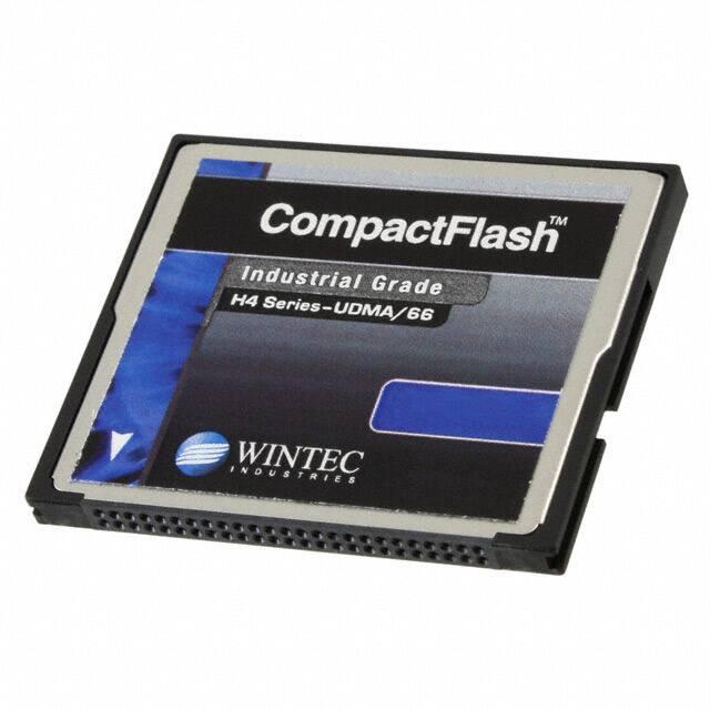
INDUSTRIAL GRADE CompactFlash Card
W7CFxxxA-H4 Series RoHS 6/6 Compliant
256MB – 32GB
CompactFlash Card
INDUSTRIAL GRADE
TM
W7CFxxxA-H4 / W8CFxxxA-H4
Series
INFORMATION IN THIS DOCUMENT IS PROVIDED IN RELATION TO
WINTEC INDUSTRIES PRODUCTS, AND IS SUBJECT TO CHANGE
WITHOUT NOTICE.
NOTHING IN THIS DOCUMENT SHALL BE CONTRUED AS GRANTING
ANY LICENSE, EXPRESS OR IMPLIED.
ALL INFORMATION IN THIS DOCUMENT IS PROVIDED ON AN “AS-IS”
BASIS WITHOUT GUARANTEE OR WARRANTY OF ANY KIND.
•
Please contact your nearest Wintec representative for the latest updates or additional product
information.
Wintec W7CFxxx-H4 and W8CFxxx-H4 Series Datasheet v1 08.doc
August 2013 Wintec Industries, Inc.
1
�TM
INDUSTRIAL GRADE CompactFlash Card
W7CFxxxA-H4 Series RoHS 6/6 Compliant
256MB – 32GB
Table of Contents
Revision History ............................................................................................................................ 3
FEATURES ................................................................................................................................ 4
DESCRIPTION........................................................................................................................... 5
1.0 General Product Specification ........................................................................................... 6
2.0
Card Function Explanation ......................................................................................... 15
2.1 Attribute Access Specifications .................................................................................. 15
2.2 Task File Register Access Specifications ................................................................... 16
2.3 Configuration Register Specification ......................................................................... 18
2.4 Task File Register Specification ................................................................................. 20
2.5 ATA Command Specification .................................................................................... 25
3.0 Electrical Specification .................................................................................................. 31
3.1 General ......................................................................................................................... 31
3.2 DC Characteristics ...................................................................................................... 34
3.3 AC Characteristics ...................................................................................................... 34
3.4 Reset Characteristics (Memory Card Mode & I/O Card Mode) ................................ 45
3.5 User Notes .................................................................................................................. 46
4.0
Physical Specifications ................................................................................................. 47
4.1 Labelling and Marking................................................................................................. 48
5.0 Ordering Information ..................................................................................................... 49
Wintec W7CFxxx-H4 and W8CFxxx-H4 Series Datasheet v1 08.doc
August 2013 Wintec Industries, Inc.
2
�TM
INDUSTRIAL GRADE CompactFlash Card
W7CFxxxA-H4 Series RoHS 6/6 Compliant
256MB – 32GB
Revision History
Revision
1.00
1.01
1.02
1.03
Month
September
October
January
February
Year
2009
2009
2010
2010
1.04
October
2011
1.05
1.06
1.07
March
July
May
2012
2012
2013
History
Initial Release (Preliminary)
Add firmware revision 090904 as option
Add firmware revision 091110a as option
Add Dual ID mode as option
Update Ordering Guide
Remove 128MB option
Added Support for Micron Flash
Updated Ordering Guide
Corrected Typo’s
Wintec W7CFxxx-H4 and W8CFxxx-H4 Series Datasheet v1 08.doc
August 2013 Wintec Industries, Inc.
3
�TM
INDUSTRIAL GRADE CompactFlash Card
W7CFxxxA-H4 Series RoHS 6/6 Compliant
256MB – 32GB
FEATURES
GENERAL
•
Density up to 32GB
•
32-bit RISC/DSP controller
•
Large internal SRAM provides firmware flexibility
•
Dual voltage support at 3.3V / 5V
•
Internal voltage detector
•
20 Kbyte internal Boot ROM and 32 Kbyte internal SRAM
•
Specialized for high-reliability
•
RoHS 6/6 compliant
RELIABILITY
•
> 2,000,000 Program/Erase Cycles
•
Industrial Wear Leveling
– Includes Static Block Management
•
Spares & Bad Block Management
•
On-Board ECC capable of correcting 4 random bytes per 512
bytes sector with additional CRC for dynamic error checking
•
High Environmental Tolerance
•
10-Year Data Retention
•
Unlimited Reads
Wintec Type I Compact Flash
(Industrial Grade H4 Series)
COMPATIBILITY
•
Fully compliance to CompactFlash TM 3.0 and compatible to 4.1 specifications
•
ATA-6 standard compatible in True-IDE mode
•
PCMCIA specification 2.1
•
Fast ATA supporting PIO mode 6, MDMA mode 4, UDMA mode 4 in True-IDE mode
•
Four integrated 8Kbyte Sector Buffers and 256 Byte PCMCIA Attribute Memory
PERFORMANCE
•
True IDE Mode Capable
– Host data transfer in PIO mode 6 or MDMA mode 4 up to 25 MByte/second
– Host data transfer in UDMA mode 4 up to 66 MByte/second
•
High Performance
– Two Direct Flash Access (DFA) Channels including two sector buffers support interleaving operation
•
Low Power Consumption:
– Maximum operation current is 130 mA (32 GB)
– Sleep mode current < 4 mA. (32 GB)
Wintec W7CFxxx-H4 and W8CFxxx-H4 Series Datasheet v1 08.doc
August 2013 Wintec Industries, Inc.
4
�TM
INDUSTRIAL GRADE CompactFlash Card
W7CFxxxA-H4 Series RoHS 6/6 Compliant
256MB – 32GB
DESCRIPTION
Wintec’s Compact Flash card is based on industrial leading Hyperstone F4 controller chip, which is a 32-bit RISC
processor with instruction set extension optimized for Flash handling. The superior wear leveling done by the
controller chip involves all physical blocks including the ones containing static data to meet the most demanding
requirements from users in a data traffic intensive environment.
The card contains a 50-pin connector consisting of two rows of 25 female contacts each on 50 mils (1.27mm)
centers. The Industrial Grade CompactFlashTM Memory Cards are constructed with Samsung or Micron single-levelcell (SLC) NAND flash memory devices. It employs a variety of sophisticated functions, such as the Reed-Solomon
error correction code which is capable of correcting up to 4 symbols in a 512 bytes sector with additional CRC for
dynamic error checking. The wear-leveling methods ensure even wear of flash blocks across the entire card
capacity. With background operations to track erase counts, the card prioritizes new writes to blocks with lower
wear, and relocates static data to blocks with higher wear. Bad-block Management routines replace worn blocks
with spare blocks reserved by the controller on card initialization. All Flash management utilities allow for
maximum levels of data reliability and card endurance for prolong life cycle.
Wintec W7CFxxx-H4 and W8CFxxx-H4 Series Datasheet v1 08.doc
August 2013 Wintec Industries, Inc.
5
�TM
INDUSTRIAL GRADE CompactFlash Card
W7CFxxxA-H4 Series RoHS 6/6 Compliant
256MB – 32GB
1.0
General Product Specification
For all the following specifications, values are defined at ambient temperature and nominal supply voltage unless
otherwise stated.
Table 1: Performance Specifications
Parameter
Burst Transfer Rate To/From Host
Burst Transfer Rate Internally To/From Flash
Sustained Sequential Read (Typical)
Sustained Sequential Write (Typical)
Random Read (Typical)
Random Write (Typical)
Table 2: Card Endurance
Parameter
Program/Erase Cycles
Read Cycles
Data Retention
MTBF
PIO Mode 6
25 MB/s
80 MB/s
18 MB/s
7.5 MB/s
TBD
TBD
Performance
UDMA Mode (Mode 4)
66 MB/s
80 MB/s
42 MB/s
20 MB/s
38MB/s
8MB/s
Table 3: Card Data Reliability
Spec
> 2,000,000 Cycles
Unlimited
10 Years (Min.)
> 4,000,000 Hours
Parameter
Non-Recoverable Errors
Erroneous Correction
ECC Correctability
Spec
< 1 in 1014 Bytes Read
< 1 in 1020 Bytes Read
4 Bytes/Sector
Table 4: Environmental Specifications
Temperature
Parameters
Standard Temp.
Industrial Temp.
Humidity
Vibration
Altitude
Shock
Acoustic
Operating
0°C to 70°C
-40°C to 85°C
8% to 95%
(Non-Condensing)
16.3 G rms
80,000 ft. (Max.)
2,000 G (Max.)
0 db
Non-Operating
-55°C to 95°C
-55°C to 95°C
8% to 95%
(Non-Condensing)
N/A
Wintec W7CFxxx-H4 and W8CFxxx-H4 Series Datasheet v1 08.doc
August 2013 Wintec Industries, Inc.
6
�TM
INDUSTRIAL GRADE CompactFlash Card
W7CFxxxA-H4 Series RoHS 6/6 Compliant
256MB – 32GB
Figure 1: Card Block Diagram
NOTE: -CE1, -CE2, -OE, -WE –IORD, -IOWR, -REG, -RESET, -CSEL, -PDIAG, -DASP pins are pulled up in card. –CE1, -CE2, -OE, -WE, IORD, -IOWR, -REG pins are Schmitt trigger type input buffer.
Wintec W7CFxxx-H4 and W8CFxxx-H4 Series Datasheet v1 08.doc
August 2013 Wintec Industries, Inc.
7
�TM
INDUSTRIAL GRADE CompactFlash Card
W7CFxxxA-H4 Series RoHS 6/6 Compliant
256MB – 32GB
Table 5: Card Pin Assignment
PC Card Memory Mode
Pin
Signal
Type
GND
Ground
1
D03
I/O
2
D04
I/O
3
D05
I/O
4
D06
I/O
5
D07
I/O
6
-CE1
I
7
A10
I
8
-OE
I
9
A09
I
10
A08
I
11
A07
I
12
VCC
Power
13
A06
I
14
A05
I
15
A04
I
16
A03
I
17
A02
I
18
A01
I
19
A00
I
20
D00
I/O
21
D01
I/O
22
D02
I/O
23
WP
O
24
-CD2
O
25
-CD1
O
26
D111
I/O
27
D121
I/O
28
D131
I/O
29
D141
I/O
30
D151
I/O
31
-CE21
I
32
-VS1
O
33
-IORD
I
34
-IOWR
I
35
-WE
I
36
RDY/BSY
O
37
VCC
Power
38
-CSEL
I
39
-VS2
O
40
RESET
I
41
-WAIT
O
42
-INPACK
O
43
-REG
I
44
BVD2
I/O
45
BVD1
I/O
46
D081
I/O
47
D091
I/O
48
D101
I/O
49
GND
Ground
50
NOTE:
1.
2.
Pin
1
2
3
4
5
6
7
8
9
10
11
12
13
14
15
16
17
18
19
20
21
22
23
24
25
26
27
28
29
30
31
32
33
34
35
36
37
38
39
40
41
42
43
44
45
46
47
48
49
50
PC Card I/O Mode
Signal
Type
GND
Ground
D03
I/O
D04
I/O
D05
I/O
D06
I/O
D07
I/O
-CE1
I
A10
I
-OE
I
A09
I
A08
I
A07
I
VCC
Power
A06
I
A05
I
A04
I
A03
I
A02
I
A01
I
A00
I
D00
I/O
D01
I/O
D02
I/O
-IOIS16
O
-CD2
O
-CD1
O
D111
I/O
D121
I/O
D131
I/O
D141
I/O
D151
I/O
-CE21
I
-VS1
O
-IORD
I
-IOWR
I
-WE
I
IREQ
O
VCC
Power
-CSEL
I
-VS2
O
RESET
I
-WAIT
O
-INPACK
O
-REG
I
-SPKR
I/O
-STSCHG
I/O
D081
I/O
D091
I/O
D101
I/O
GND
Ground
Pin
1
2
3
4
5
6
7
8
9
10
11
12
13
14
15
16
17
18
19
20
21
22
23
24
25
26
27
28
29
30
31
32
33
34
35
36
37
38
39
40
41
42
43
44
45
46
47
48
49
50
True IDE Mode
Signal
Type
GND
Ground
D03
I/O
D04
I/O
D05
I/O
D06
I/O
D07
I/O
-CS0
I
A102
I
-ATA SEL
I
A092
I
A082
I
A072
I
VCC
Power
A062
I
A052
I
A042
I
A032
I
A02
I
A01
I
A00
I
D00
I/O
D01
I/O
D02
I/O
-IOCS16
O
-CD2
O
-CD1
O
D111
I/O
D121
I/O
D131
I/O
D141
I/O
D151
I/O
-CS11
I
-VS1
O
-IORD
I
-IOWR
I
-WE3
I
INTRQ
O
VCC
Power
-CSEL
I
-VS2
O
RESET
I
IORDY
O
DMARQ
O
-DMACK
I
-DASP
I/O
-PDIAG
I/O
D081
I/O
D091
I/O
D101
I/O
GND
Ground
These signals are required only for 16-bit access and not required when installed in 8-bit systems. For lowest power dissipation, leave
these signals open.
Should be grounded by the host.
Wintec W7CFxxx-H4 and W8CFxxx-H4 Series Datasheet v1 08.doc
August 2013 Wintec Industries, Inc.
8
�TM
INDUSTRIAL GRADE CompactFlash Card
W7CFxxxA-H4 Series RoHS 6/6 Compliant
256MB – 32GB
3.
Should be tied to VCC by the host.
Table 6: Card Pin Explanation
Signal Name
Type
Pin #
A10 - A0
(PC Card Memory Mode)
8, 10, 11, 12, 14 -20
A10 - A0
(PC Card I/O Mode)
Description
These address lines along with the –REG signal are used to
select the following: The I/O port address registers within the
Compact Flash Card, the memory mapped port address
registers within the card, a byte in the card’s information
structure and its configuration control and status registers.
This signal is the same as the PC Card Memory Mode signal.
I
A2 - A0
(True IDE Mode)
In True IDE Mode only A [2:0] is used to select the one of
eight registers in the Task File.
18, 19, 20
A10 - A3
(True IDE Mode)
In True IDE Mode these remaining address lines should be
grounded by the host.
BVD1
(PC Card Memory Mode)
This signal is asserted high as the BVD1 signal since a
battery is not used with this product.
-STSCHG
(PC Card I/O Mode)
Status Changed
This signal is asserted low to alert the host to changes in the
RDY/ -BSY and Write Protect states, while the I/O interface
is configured. Its use is controlled by the Card Config and
Status Register.
I/O
46
-PDIAG
(True IDE Mode)
In the True IDE Mode, this input/output is the Pass
Diagnostic signal in the Master/Slave handshake protocol.
BVD2
(PC Card Memory Mode)
This output line is always driven to a high state in Memory
Mode since a battery is not required for this product.
-SPKR
(PC Card I/O Mode)
I/O
45
This output line is always driven to a high state in I/O Mode
since this product does not support the audio function.
-DASP
(True IDE Mode)
In the True IDE Mode, this input/output is the Disk
Active/Slave Present signal in the Master/Slave handshake
protocol.
-CD1, -CD2
(PC Card Memory Mode)
These Card Detect pins are connected to ground on the
Compact Flash Card. They are used by the host to determine
if the card is fully inserted into its socket.
-CD1, -CD2
(PC Card I/O Mode)
O
25, 26
-CD1, -CD2
(True IDE Mode)
This signal is the same for all modes.
This signal is the same for all modes.
Wintec W7CFxxx-H4 and W8CFxxx-H4 Series Datasheet v1 08.doc
August 2013 Wintec Industries, Inc.
9
�TM
INDUSTRIAL GRADE CompactFlash Card
W7CFxxxA-H4 Series RoHS 6/6 Compliant
256MB – 32GB
Table 6: Card Pin Explanation Cont.
Signal Name
Type
Pin #
I
7, 32
-CE1, -CE2
(PC Card Memory Mode)
Card Enable
-CE1, -CE2
(PC Card I/O Mode)
Card Enable
Description
These input signals are used both to select the card and to
indicate to the card whether a byte or a word operation is
being performed. –CE2 always accesses the odd byte of the
word. –CE1 accesses the even byte or the Odd byte of the
word depending on A0 and –CE2. A multiplexing scheme
based on A0, -CE1, -CE2 allows 8 bit hosts to access all data
on D0 -D7.
This signal is the same as the PC Card Memory Mode signal.
-CS0, -CS1
(True IDE Mode)
In the True IDE Mode –CS0 is the chip select for the task file
registers while –CS1 is used to select the Alternate Status
Register and the Device Control Register.
-CSEL
(PC Card Memory Mode)
This signal is not used for this mode.
-CSEL
(PC Card I/O Mode)
I
39
This signal is not used for this mode.
-CSEL
(True IDE Mode)
This internally pulled up signal is used to configure this
device as a Master or a Slave when configured in the True
IDE Mode. When this pin is grounded, this device is
configured as a Master. When this pin is open, this device is
configured as a Slave.
D15 - D00
(PC Card Memory Mode)
These lines carry the Data, Commands and Status
information between the host and the controller. D00 is the
LSB of the Even Byte of the Word. D08 is the LSB of the
Odd Byte of the Word.
D15 - D00
(PC Card I/O Mode)
I/O
2-6, 21, 22, 23,
27-31, 47, 48, 49
These signals are the same as the PC Card Memory Mode
signal.
D15 - D00
(True IDE Mode)
In True IDE Mode all Task File operations occur in byte
mode on the low order bus D00 -D07 while all data transfers
are 16 bits using D00 -D15.
GND
(PC Card Memory Mode)
Ground.
GND
(PC Card I/O Mode)
-
1, 50
GND
(True IDE Mode)
This signal is the same for all modes.
This signal is the same for all modes.
Wintec W7CFxxx-H4 and W8CFxxx-H4 Series Datasheet v1 08.doc
August 2013 Wintec Industries, Inc.
10
�TM
INDUSTRIAL GRADE CompactFlash Card
W7CFxxxA-H4 Series RoHS 6/6 Compliant
256MB – 32GB
-INPACK
(PC Card Memory Mode)
This signal is not used in this mode.
-INPACK
(PC Card I/O Mode)
Input Acknowledge
The Input Acknowledge signal is asserted by the Compact
Flash Card when the card is selected and responding to an I/O
read cycle at the address that is on the address bus. This
signal is used by the host to control the enable of any input
data buffers between the card and the CPU.
This signal is a DMA Request that is used for DMA data
transfers between host and device. It shall be asserted by the
device when it is ready to transfer data to or from the host.
For Multiword DMA transfers, the direction of data transfer
is controlled by DIOR- and DIOW-.This signal is used in a
handshake manner with DMACK- before negating
DMAREQ, and reasserting DMAREQ if there is more data to
transfer.
O
43
DMAREQ shall not be driven when the device is not
selected.
While a DMA operation is in progress, -CS0 and –CS1 shall
be held negated and the width of the transfers shall be 16 bits.
DMARQ
(True IDE Mode)
If there is no hardware support for DMA mode in the host,
this output signal is not used and should not be connected at
the host .In this case, the BIOS must report that DMA mode
is not supported by the host so that the device driver will not
attempt DMA mode.
A host that does not support DMA mode and implements
both PCMCIA and true-IDE modes of operation need not
alter the PCMICIA mode connections while in True-IED
mode as long as this does not prevent proper operation in any
mode.
-IORD
(PC Card Memory Mode)
-IORD
(PC Card I/O Mode)
This signal is not used in this mode.
I
34
-IORD
(True IDE Mode)
This is an I/O Read strobe generated by the host. This signal
gates I/O data onto the bus from the Compact Flash Card
when the card is configured to use the I/O interface.
In True IDE Mode, this signal has the same function as in PC
Card I/O Mode.
Wintec W7CFxxx-H4 and W8CFxxx-H4 Series Datasheet v1 08.doc
August 2013 Wintec Industries, Inc.
11
�TM
INDUSTRIAL GRADE CompactFlash Card
W7CFxxxA-H4 Series RoHS 6/6 Compliant
256MB – 32GB
Table 6: Card Pin Explanation Cont.
Signal Name
Type
Pin #
Description
-IOWR
(PC Card Memory Mode)
This signal is not used in this mode.
- IOWR
(PC Card I/O Mode)
The I/O Write strobe pulse is used to clock I/O data on the
Card Data bus into the Compact Flash controller registers
when the card is configured to use the I/O interface.
The clocking will occur on the negative to positive edge of
the signal (trailing edge).
I
35
- IOWR
(True IDE Mode)
In True IDE Mode, this signal has the same function as in PC
Card I/O Mode.
-OE
(PC Card Memory Mode)
This is an Output Enable strobe generated by the host
interface. It is used to read data from the Compact Flash Card
in Memory Mode and to read the CIS and configuration
registers.
-OE
(PC Card I/O Mode)
I
9
-ATA SEL
(True IDE Mode)
In PC Card I/O Mode, this signal is used to read the CIS and
configuration registers.
To enable True IDE Mode this input should be grounded by
the host.
In Memory Mode this signal is set high when the Compact
Flash Card is ready to accept a new data transfer operation
and held low when the card is busy. The host memory card
socket must provide a pull-up resistor.
RDY/-BSY
(PC Card Memory Mode)
O
37
- IREQ
(PC Card I/O Mode)
-INTRQ
(True IDE Mode)
At power up and at Reset, the RDY/-BSY signal is held low
(busy) until the Compact Flash Card has completed its power
up or reset function. The RDY/-BSY signal is held high
(disabled from being busy) whenever the following condition
is true: The Compact Flash Card has been powered up with
+RESET continuously disconnected or asserted.
I/O Operation – After the Compact Flash Card has been
configured for I/O operation, this signal is used as – Interrupt
Request. This line is strobed low to generate a pulse mode
interrupt or held low for a level mode interrupt.
In True IDE Mode, this signal is the active high Interrupt
Request to the host.
Wintec W7CFxxx-H4 and W8CFxxx-H4 Series Datasheet v1 08.doc
August 2013 Wintec Industries, Inc.
12
�TM
INDUSTRIAL GRADE CompactFlash Card
W7CFxxxA-H4 Series RoHS 6/6 Compliant
256MB – 32GB
Table 6: Card Pin Explanation Cont.
Signal Name
Type
Pin #
-REG
(PC Card Memory Mode)
Attribute Memory Select
Description
This signal is used during Memory Cycles to distinguish
between Common Memory and Register (Attribute) Memory
accesses. High for Common Memory, Low for Attribute
Memory.
The signal must also be active (low) during I/O Cycles when
the I/O address is on the Bus.
-REG
(PC Card I/O Mode)
This is a DMA Acknowledge signal that is asserted by the
host in response to DMAREQ to initiate DMA transfers.
I
44
While DMA operations are not active, the card shall ignore
the –DMACK signal, including a floating condition.
If DAM operation is not supported by a True-IDE Mode only
host, this signal should be driven high or connected to VCC
by the host.
-DMACK
(True IDE Mode)
A host that does not support DMA mode and implements
both PCMCIA and True-IDE modes of operation need not
alter the PCMCIA mode connections while in True-IDE
mode as long as this does not prevent proper operation all
modes.
RESET
(PC Card Memory Mode)
I
41
RESET
(PC Card I/O Mode)
This signal is the same as the PC Card Memory Mode signal.
In the True IDE Mode this input pin is the active low
hardware reset from the host.
-RESET
(True IDE Mode)
VCC
(PC Card Memory Mode)
VCC
(PC Card I/O Mode)
When the pin is high, this signal resets the Compact Flash
Card. The card is Reset only at power up if this pin is left
high or open from power-up. The card is also reset when the
Soft Reset bit in the Card Configuration Option Register is
set.
+5, +3.3V power.
-
13, 38
This signal is the same for all modes.
VCC
(True IDE Mode)
This signal is the same for all modes.
-VS1, -VS2
(PC Card Memory Mode)
Voltage Sense Signals. –VS1 is grounded so that the
Compact Flash Card CIS can be read at 3.3 volts and –VS2 is
open and reserved by PCMCIA for a secondary voltage.
-VS1, -VS2
(PC Card I/O Mode)
O
33, 40
-VS1, -VS2
(True IDE Mode)
This signal is the same for all modes.
This signal is the same for all modes.
Wintec W7CFxxx-H4 and W8CFxxx-H4 Series Datasheet v1 08.doc
August 2013 Wintec Industries, Inc.
13
�TM
INDUSTRIAL GRADE CompactFlash Card
W7CFxxxA-H4 Series RoHS 6/6 Compliant
256MB – 32GB
Table 6: Card Pin Explanation Cont.
Signal Name
Type
Pin #
-WAIT
(PC Card Memory Mode)
-WAIT
(PC Card I/O Mode)
Description
This signal is not asserted for all modes.
O
42
This signal is not asserted for all modes.
-IORDY
(True IDE Mode)
This signal is not asserted for all modes.
-WE
(PC Card Memory Mode)
This is a signal driven by the host and used for strobing
memory write data to the registers of the Compact Flash Card
when the card is configured in the memory interface mode. It
is also used for writing the configuration registers.
-WE
(PC Card I/O Mode)
I
36
In PC Card I/O Mode, this signal is used for writing the
configuration registers.
-WE
(True IDE Mode)
In True IDE Mode this input signal is not used and should be
connected to VCC by the host.
-WP
(PC Card Memory Mode)
Memory Mode – The Compact Flash Card does not have a
write protect switch. This signal is held low after the
completion of the reset initialization sequence.
-IOIS16
(PC Card I/O Mode)
I/O Operation – When the Compact Flash Card is configured
for I/O Operation, Pin 24 is used for the –I/O Selected is 16
Bit Port (-IOIS16) function. A Low signal indicates that a 16
bit or odd byte only operation can be performed at the
addressed port.
O
24
-IOCS16
(True IDE Mode)
In True IDE Mode this output signal is asserted low when
this device is expecting a word data transfer cycle.
Wintec W7CFxxx-H4 and W8CFxxx-H4 Series Datasheet v1 08.doc
August 2013 Wintec Industries, Inc.
14
�TM
INDUSTRIAL GRADE CompactFlash Card
W7CFxxxA-H4 Series RoHS 6/6 Compliant
256MB – 32GB
2.0
Card Function Explanation
2.1
Attribute Access Specifications
When CIS-ROM region or Configuration register region is accessed, read and write operations are executed under
the condition of –REG = “L” as follows. That region can be accessed by Byte/Word/Odd-byte modes, which are
defined by PC card standard specifications.
Table 7: Attribute Read Access Mode
Mode
Standby mode
-REG
L
L
L
L
Byte access (8-bit)
Word access (16-bit)
Odd byte access (8-bit)
-CE2
H
H
H
L
L
-CE1
A0
-OE
-WE
L
L
L
H
L
H
L
L
L
L
H
H
H
H
-CE1
A0
-OE
-WE
L
L
L
H
L
H
H
H
H
H
L
L
L
L
D8 -D15
High-Z
High-Z
High-Z
Invalid
Invalid
D0 -D7
High-Z
Even byte
Invalid
Even byte
High-Z
D8 -D15
Don’t care
Don’t care
Don’t care
Don’t care
Don’t care
D0 -D7
Don’t care
Even byte
Don’t care
Even byte
Don’t care
Table 8: Attribute Write Access Mode
Mode
Standby mode
Byte access (8-bit)
-REG
Word access (16-bit)
Odd byte access (8-bit)
L
L
L
L
-CE2
H
H
H
L
L
Figure 2: Attribute Access Timing Example
Wintec W7CFxxx-H4 and W8CFxxx-H4 Series Datasheet v1 08.doc
August 2013 Wintec Industries, Inc.
15
�TM
INDUSTRIAL GRADE CompactFlash Card
W7CFxxxA-H4 Series RoHS 6/6 Compliant
256MB – 32GB
2.2
Task File Register Access Specifications
There are two cases of Task File register mapping, one is mapped I/O address area, and the other is mapped Memory
address area. Each case of Task File register read and write operations are executed under the condition as follows.
That area can be accessed by Byte/Word/Odd Byte modes, which are defined by PC card standard specifications.
2.2.1 I/O Address Map
Table 9: Task File Register Read Access Mode (i)
Mode
Standby mode
Byte access (8-bit)
Word access (16-bit)
Odd byte access (8-bit)
-REG -CE2 -CE1
H
L
H
L
L
H
L
L
L
L
L
L
H
A0
L
H
-IORD -IOWR
L
L
L
L
H
H
H
H
-OE -WE
H
H
H
H
H
H
H
H
D8 -D15
High-Z
High-Z
High-Z
Odd byte
Odd byte
D0 -D7
High-Z
Even byte
Odd byte
Even byte
High-Z
D8 -D15
Don’t care
Don’t care
Don’t care
Odd byte
Odd byte
D0 -D7
Don’t care
Even byte
Odd byte
Even byte
Don’t care
Table 10: Task File Register Write Access Mode (i)
Mode
Standby mode
Byte access (8-bit)
Word access (16-bit)
Odd byte access (8-bit)
-REG -CE2 -CE1
H
L
H
L
L
H
L
L
L
L
L
L
H
A0
L
H
-IORD -IOWR
H
H
H
H
L
L
L
L
-OE -WE
H
H
H
H
H
H
H
H
Figure 3: Task File Register Access Timing Example (i)
2.2.2 Memory Address Map
Table 11: Task File Register Read Access Mode (ii)
Mode
Standby mode
Byte access (8-bit)
Word access (16-bit)
Odd byte access (8-bit)
-REG -CE2 -CE1
H
H
H
L
H
H
L
H
L
L
H
L
H
A0
L
H
-IORD -IOWR
L
L
L
L
H
H
H
H
-OE -WE
H
H
H
H
H
H
H
H
D8 -D15
High-Z
High-Z
High-Z
Odd byte
Odd byte
D0 -D7
High-Z
Even byte
Odd byte
Even byte
High-Z
Wintec W7CFxxx-H4 and W8CFxxx-H4 Series Datasheet v1 08.doc
August 2013 Wintec Industries, Inc.
16
�TM
INDUSTRIAL GRADE CompactFlash Card
W7CFxxxA-H4 Series RoHS 6/6 Compliant
256MB – 32GB
Table 12: Task File Register Write Access Mode (ii)
Mode
Standby mode
-REG -CE2 -CE1
H
H
H
L
H
H
L
H
L
L
H
L
H
Byte access (8-bit)
Word access (16-bit)
Odd byte access (8-bit)
A0
L
H
-IORD -IOWR
H
H
H
H
L
L
L
L
-OE -WE
H
H
H
H
H
H
H
H
D8 -D15
Don’t care
Don’t care
Don’t care
Odd byte
Odd byte
D0 -D7
Don’t care
Even byte
Odd byte
Even byte
Don’t care
Figure 4: Task File Register Access Timing Example (ii)
2.2.3 True IDE Mode
The card can be configured in a True IDE Mode of operation. This card is configured in this mode only when the –
OE input signal is asserted GND by the host. In this True IDE Mode Attribute Registers are not accessible from the
host. Only I/O operation to the task files and data registers are allowed. If this card is configured during power on
sequence, data registers are accessed in word (16-bit). The card permits 8-bit accesses if the user issues a Set Feature
Command to put the device in 8-bit mode.
Table 13: True IDE Mode Read I/O Function
Mode
Invalid mode
Standby mode
Data register access
Alternate status access
Other task file access
-CE2
L
H
H
L
H
-CE1
L
H
L
H
L
A0 -A2
-IORD
-IOWR
0
6H
1-7H
L
L
L
H
H
H
A0 -A2
-IORD
-IOWR
0
6H
1-7H
L
L
L
H
H
H
D8 -D15
High-Z
High-Z
Odd byte
High-Z
High-Z
D0 -D7
High-Z
High-Z
Even byte
Status out
Data
D8 -D15
Don’t care
Don’t care
Odd byte
Don’t care
Don’t care
D0 -D7
Don’t care
Don’t care
Even byte
Control in
Data
Table 14: True IDE Mode Write I/O Function
Mode
Invalid mode
Standby mode
Data register access
Alternate status access
Other task file access
-CE2
L
H
H
L
H
-CE1
L
H
L
H
L
Wintec W7CFxxx-H4 and W8CFxxx-H4 Series Datasheet v1 08.doc
August 2013 Wintec Industries, Inc.
17
�TM
INDUSTRIAL GRADE CompactFlash Card
W7CFxxxA-H4 Series RoHS 6/6 Compliant
256MB – 32GB
Figure 5: True IDE Mode I/O Access Timing Example
2.3
Configuration Register Specification
This card supports four configuration registers for the purpose of the configuration and observation of this card.
These registers can be used in memory card mode and I/O card mode. In True IDE mode, these registers cannot be
used.
2.3.1 Configuration Option register (Address 200H)
This register is used for setting the card configuration status and for issuing soft reset to the card.
bit 7
SRESET
NOTE:
1.
bit 6
LevlREQ
bit 5
INDEX
bit 4
bit 3
bit 2
bit 1
bit 0
Initial value: 00H
Table 15: Option Register Function
Name
R/W
Function
Setting this bit to “1”, places the card in the reset state (Card Hard Reset). This
operation is equal to Hard Reset, except this bit is not cleared. Then this bit set to
“0”, places the card in the reset state of Hard Reset (This bit is set to “0” by Hard
Reset). Card configuration status is reset and the card internal initialized operation
starts when Card hard Reset is executed, so next access to the card should be the
same sequence as the power on sequence.
SRESET (HOST->)
R/W
LevlREQ (HOST->)
R/W
This bit sets to “0” when pulse mode interrupt is selected, and “1” when level mode
interrupt is selected.
INDEX (HOST->)
R/W
This bit is used for select operation mode of the card as follows. When Power on,
Card Hard Reset and Soft Reset, this data is “000000” for the purpose of Memory
card interface recognition.
Table 16: INDEX bit assignment
5
0
0
0
4
0
0
0
INDEX Bit
3
2
0
0
0
0
0
0
1
0
0
1
0
0
1
0
Task File register address
Mapping mode
0H to FH, 400H to 7FFH
xx0H to xxFH
1F0H to 1F7H, 3F6H to 3F7H
Memory Mapped
Contiguous I/O Mapped
Primary I/O Mapped
Wintec W7CFxxx-H4 and W8CFxxx-H4 Series Datasheet v1 08.doc
August 2013 Wintec Industries, Inc.
18
�TM
INDUSTRIAL GRADE CompactFlash Card
W7CFxxxA-H4 Series RoHS 6/6 Compliant
256MB – 32GB
0
0
0
0
1
1
170H to 177H, 376H to 377H
Secondary I/O Mapped
2.3.2 Configuration and Status Register (Address 202H)
This register is used for observing the card state.
bit 7
CHGED
bit 6
SIGCHG
bit 5
IOIS8
bit 4
0
bit 3
0
bit 2
PWD
bit 1
INTR
bit 0
0
NOTE:
1. 1nitial value: 00H
Table 17: Configuration and Status Register Function
Name
R/W
CHGED (HOST->)
R
SIGCHG (HOST->)
R/W
IOIS8 (HOST->)
R/W
PWD (HOST->)
R/W
INTR (HOST->)
R
Function
This bit indicates that CRDY/-BSY bit on Pin Replacement register is set to “1”.
When CHGED bit is set to “1”, -STSCHG pin is held “L” at the condition of
SIGCHG bit set to “1” and the card configured for the I/O interface.
This bit is set or reset by the host for enabling and disabling the status-change signal
(-STSCHG pin). When the card is configured I/O card interface and this bit is set to
“1”, -STSCHG pin is controlled by CHGED bit. If this bit is set to “0”, -STSCHG
pin is kept “H”.
The host sets this field to “1” when it can provide I/O cycles only with one 8-bit
data bus (D7 to D0).
When this bit is set to “1”, the card enters sleep stat (Power Down mode). When
this bit is reset to “0”, the card transfers to idle state (active mode). RRDY/-BSY bit
on Pin Replacement Register becomes BUSY when this bit is changed. RRDY/BSY will not become Ready until the power state requested has been entered. This
card automatically powers down when it is idle, and powers back up when it
receives a command.
This bit indicates the internal state of the interrupt request. This bit state is available
whether I/O card interface has been configured or not. This signal remains true until
the condition which caused the interrupt request has been serviced. If interrupts are
disabled by the –IEN bit in the Device Control Register, this bit is a zero.
2.3.3 Pin Replacement Register (Address 204H)
This register is used for providing the signal state of –IREQ signal when the card configured I/O card interface.
bit 7
0
bit 6
0
bit 5
CRDY/-BSY
bit 4
0
bit 3
1
bit 2
1
bit 1
RRDY/-BSY
bit 0
0
NOTE:
1. Initial value 0CH
Table 18: Pin Replacement Register Function
Name
R/W
CRDY/-BSY (HOST->)
R/W
RRDY/-BSY (HOST->)
R/W
Function
This bit is set to “1” when the RRDY/-BSY bit changes state. This bit may also be
written by the host
When read, this bit indicates +READY pin states. When written, this bit is used for
CRDY/-BSY bit masking
Wintec W7CFxxx-H4 and W8CFxxx-H4 Series Datasheet v1 08.doc
August 2013 Wintec Industries, Inc.
19
�TM
INDUSTRIAL GRADE CompactFlash Card
W7CFxxxA-H4 Series RoHS 6/6 Compliant
256MB – 32GB
2.3.4 Socket and Copy Register (Address 206H)
This register is used for identification of the card from the other cards. Host can read and write this register. This
register should be set by host before Configuration Option register is set.
bit 7
0
bit 6
0
bit 5
0
bit 4
DRV#
bit 3
0
bit 2
0
bit 1
0
bit 0
0
NOTE:
1. Initial value: 00H
Table 19: Socket and Copy Register Function
Name
R/W
DRV# (HOST->)
2.4
Function
This field is used for the configuration of the plural cards. When host configures the
plural cards, written the card’s copy number in this field. In this way, host can
perform the card’s master/slave organization.
R/W
Task File Register Specification
These registers are used for reading and writing the storage data in the card. These registers are mapped five types
by the configuration of INDEX in Configuration Option register. The decoded addresses are shown as follows.
Table 20: Memory map (INDEX=0)
-REG
1
1
1
1
1
1
1
1
1
1
1
1
1
1
1
A10
0
0
0
0
0
0
0
0
0
0
0
0
0
1
1
A9 -A4
A3
0
0
0
0
0
0
0
1
1
1
1
1
1
A2
0
0
0
0
1
1
1
1
0
0
1
1
1
A1
0
0
0
0
1
1
1
1
0
0
1
1
1
A0
0
1
0
1
0
1
0
1
0
1
1
0
1
0
1
Offset
0H
1H
2H
3H
4H
5H
6H
7H
8H
9H
DH
EH
FH
8H
9H
-OE=L
Data register
Error register
Sector count register
Sector number register
Cylinder low register
Cylinder high register
Drive head register
Status register
Dup. even data register
Dup. odd data register
Dup. error register
Alt. status register
Drive address register
Even data register
Odd data register
-WE=L
Data register
Feature register
Sector count register
Sector number register
Cylinder low register
Cylinder high register
Drive head register
Command register
Dup. even data register
Dup. odd data register
Dup. feature register
Device control register
Reserved
Even data register
Odd data register
Table 21: Contiguous I/O map (INDEX=1)
-REG
0
0
0
0
0
0
0
0
0
0
0
A10 -A4
A3
0
0
0
0
0
0
0
0
1
1
1
A2
0
0
0
0
1
1
1
1
0
0
1
A1
0
0
1
1
0
0
1
1
0
0
0
A0
0
1
0
1
0
1
0
1
0
1
1
Offset
0H
1H
2H
3H
4H
5H
6H
7H
8H
9H
DH
-IORD=L
Data register
Error register
Sector count register
Sector number register
Cylinder low register
Cylinder high register
Drive head register
Status register
Dup. even data register
Dup. odd data register
Dup. error register
-IOWR=L
Data register
Feature register
Sector count register
Sector number register
Cylinder low register
Cylinder high register
Drive head register
Command register
Dup. even data register
Dup. odd data register
Dup. feature register
Wintec W7CFxxx-H4 and W8CFxxx-H4 Series Datasheet v1 08.doc
August 2013 Wintec Industries, Inc.
20
�TM
INDUSTRIAL GRADE CompactFlash Card
W7CFxxxA-H4 Series RoHS 6/6 Compliant
256MB – 32GB
0
0
1
1
1
1
1
1
0
1
EH
FH
Alt. status register
Drive address register
Device control register
Reserved
Table 22: Primary I/O Map (INDEX=2)
-REG
0
0
0
0
0
0
0
0
0
0
A10
A9 -A4
1FH
1FH
1FH
1FH
1FH
1FH
1FH
1FH
3FH
3FH
A3
0
0
0
0
0
0
0
0
0
0
A2
0
0
0
0
1
1
1
1
1
1
A1
0
0
1
1
0
0
1
1
1
1
A0
0
1
0
1
0
1
0
1
0
1
-IORD=L
Data register
Error register
Sector count register
Sector number register
Cylinder low register
Cylinder high register
Drive head register
Status register
Alt. status register
Drive address register
-IOWR=L
Data register
Feature register
Sector count register
Sector number register
Cylinder low register
Cylinder high register
Drive head register
Command register
Device control register
Reserved
Table 23: Secondary I/O Map (INDEX=3)
-REG
0
0
0
0
0
0
0
0
0
0
A10
A9 -A4
17H
17H
17H
17H
17H
17H
17H
17H
37H
37H
A3
0
0
0
0
0
0
0
0
0
0
A2
0
0
0
0
1
1
1
1
1
1
A1
0
0
1
1
0
0
1
1
1
1
Table 24: True IDE Mode I/O Map
-CE2
1
1
1
1
1
1
1
1
0
0
-CE1
0
0
0
0
0
0
0
0
1
1
A2
0
0
0
0
1
1
1
1
1
1
A1
0
0
1
1
0
0
1
1
1
1
A0
0
1
0
1
0
1
0
1
0
1
-IORD=L
Data register
Error register
Sector count register
Sector number register
Cylinder low register
Cylinder high register
Drive head register
Status register
Alt. status register
Drive address register
-IOWR=L
Data register
Feature register
Sector count register
Sector number register
Cylinder low register
Cylinder high register
Drive head register
Command register
Device control register
Reserved
2.4.1 Data Register
This register is a 16-bit register that has read/write ability, and it is used for transferring 1 sector data between the
card and the host. This register can be accessed in word mode and byte mode. This register overlaps the Error and
Feature register.
bit 15 bit 14 bit 13 bit 12 bit 11 bit 10
bit 9
bit 8 bit 7
D0 to D15
bit 6
bit 5
bit 4
bit 3
bit 2
bit 1
bit 0
Wintec W7CFxxx-H4 and W8CFxxx-H4 Series Datasheet v1 08.doc
August 2013 Wintec Industries, Inc.
21
�TM
INDUSTRIAL GRADE CompactFlash Card
W7CFxxxA-H4 Series RoHS 6/6 Compliant
256MB – 32GB
2.4.2 Error Register
This register is a read only register, and is used for analyzing the error content during card accessing. This register is
valid when the BSY bit in Status Register and Alternate Status Register are set to “0” (Ready).
bit 7
BBK
bit 6
UNC
bit 5
“0”
bit 4
IDNF
bit 3
“0”
bit 2
ABRT
bit 1
‘0’
bit 0
AMNF
Table 25: Error Register Function
bit
7
6
4
2
0
Name
BBK (Bad BlocK detected)
UNC (Data ECC error)
IDNF (ID Not Found)
ABRT (AboRTed command)
AMNF (Address Mark Not Found)
Function
This bit is set when a Bad Block is detected in requested ID field.
This bit is set when Uncorrectable error is occurred at reading the card.
The requested sector ID is in error or cannot be found.
This bit is set if the command has been aborted because of the card
status condition. (Not ready, Write fault, Invalid command, etc.)
This bit is set in case of a general error.
2.4.3 Feature Register
This register is a write only register, and provides information regarding features of the drive, which the host wishes
to utilize.
bit 7
bit 6
bit 5
bit 4
bit 3
Feature byte
bit 2
bit 1
bit 0
2.4.4 Sector Count Register
This register contains the numbers of sectors of data requested to be transferred on a read or write operation between
the host and the card. If the value of this register is zero, a count of 256 sectors is specified. In plural sector transfer,
if not successfully completed, the register contains the number of sectors, which need to be transferred in order to
complete, the request. This register’s initial value is “01H”.
bit 7
bit 6
bit 5
bit 4
bit 3
Sector count byte
bit 2
bit 1
bit 0
2.4.5 Sector Number Register
This register contains the starting sector number, which is started by following sector transfer command.
bit 7
bit 6
bit 5
bit 4
bit 3
Sector number byte
bit 2
bit 1
bit 0
2.4.6 Cylinder Low Register
This register contains the low 8-bit of the starting cylinder address, which is started by following sector transfer
command.
bit 7
bit 6
bit 5
bit 4
bit 3
Cylinder low byte
bit 2
bit 1
bit 0
2.4.7 Cylinder High Register
This register contains the high 8-bit of the starting cylinder address, which is started by following sector transfer
command.
Wintec W7CFxxx-H4 and W8CFxxx-H4 Series Datasheet v1 08.doc
August 2013 Wintec Industries, Inc.
22
�TM
INDUSTRIAL GRADE CompactFlash Card
W7CFxxxA-H4 Series RoHS 6/6 Compliant
256MB – 32GB
bit 7
bit 6
bit 5
bit 4
bit 3
Cylinder high byte
bit 2
bit 1
bit 0
2.4.8 Drive Head Register
This register is used for selecting the Drive number and head number for the following command.
bit 7
1
NOTE:
1.
bit 6
LBA
bit 5
1
bit 4
DRV
bit 3
Head #
bit 2
bit 1
bit 0
DRV: Drive number
Table 26: Drive Head Register Function
bit
7
Name
1
6
LBA
5
1
4
DRV (DRiVe select)
3 -0
Head number
Function
This bit is set to “1”.
LBA is a flag to select either Cylinder / Head / Sector (CHS) or Logical Block
Address (LBA) mode. When LBA = 0, CHS mode is selected. When LBA = 1, LBA
mode is selected. In LBA mode, the Logical Block Address is interrupted as follows:
LBA07 - LBA00: Sector Number Register D7 - D0.
LBA15 - LBA08: Cylinder Low Register D7 - D0.
LBA23 - LBA16: Cylinder High Register D7 - D0.
LBA27 - LBA24: Drive / Head Register bits HS3 - HS0.
This bit is set to “1”.
This bit is used for selecting the Master (Card 0) and Slave (Card 1) in Master/Slave
organization. The card is set to be Card 0 or 1 by using DRV# of the Socket and Copy
register.
This bit is used for selecting the Head number for the following command. Bit 3 is
MSB.
2.4.9 Status Register
This register is read only register, and it indicates the card status of command execution. When this register is read
in configured I/O card mode (INDEX = 1, 2, 3) and level interrupt mode, -IREQ is negated. This register should be
accessed in byte mode. In word mode, it is recommended that Alternate status register may be used as this register.
bit 7
BSY
bit 6
DRDY
bit 5
DWF
bit 4
DSC
bit 3
DRQ
bit 2
CORR
bit 1
IDX
bit 0
ERR
Table 27: Status Register Function
bit
Name
7
BSY (BuSY)
6
DRDY (Drive ReaDY)
5
4
DWF (Drive Write Full)
DSC (Drive Seek Complete)
3
DRQ (Data ReQuest)
2
CORR (CORRected data)
1
IDX (InDeX)
0
ERR (ERRor)
Function
This bit is set when the card internal operation is executing. When this bit is set
to “1”, other bits in this register are invalid.
If this bit and DSC bit are set to “1”, the card is capable of receiving the read
or write or seek requests. If this bit is set to “0”, the card prohibits these
requests.
This bit is set if this card indicates the write fault status.
This bit is set when the drive seek complete.
This bit is set when the information can be transferred between the host and
Data register. This bit is cleared when the card receives the other command.
This bit is set when a correctable data error has been occurred and the data has
been corrected.
This bit is always set to “0”.
This bit is set when the previous command has ended in some type of error.
The error information is set in the other Status register or Error register. This
bit is cleared by the next command.
Wintec W7CFxxx-H4 and W8CFxxx-H4 Series Datasheet v1 08.doc
August 2013 Wintec Industries, Inc.
23
�TM
INDUSTRIAL GRADE CompactFlash Card
W7CFxxxA-H4 Series RoHS 6/6 Compliant
256MB – 32GB
2.4.10 Alternate Status Register
This register is the same as Status register in physically, so the it assignment refers to previous item of Status
register. But this register is different from Status register that –IREQ is not negated when data read.
2.4.11 Command Register
This register is write only register, and it is used for writing the command at executing the drive operation. The
command code written in the command register, after the parameter is written in the Task File during the card is
Ready state.
Table 28: Command Register
Command
Command Code
Check power mode
Execute drive diagnostic
Erase sector
Format track
Identify Drive
Idle
Idle immediate
Initialize drive parameters
Read buffer
Read multiple
Read long sector
Read sector
Read verify sector
Recalibrate
Request sense
Seek
Set features
Set multiple mode
Set sleep mode
Stand by
Stand by immediate
Translate sector
Wear level
Write buffer
Write long sector
Write multiple
Write multiple w/o erase
Write sector
Write sector w/o erase
Write verify
E5H or 98H
90H
C0H
50H
ECH
E3H or 97H
E1H or 95H
91H
E4H
C4H
22H or 23H
20H or 21H
40H or 41H
1XH
03H
7XH
EFH
C6H
E6H or 99H
E2H or 96H
E0H or 94H
87H
F5H
E8H
32H or 33H
C5H
CDH
30H or 31H
38H
3CH
FR
N
N
N
N
N
N
N
N
N
N
N
N
N
N
N
N
Y
N
N
N
N
N
N
N
N
N
N
N
N
N
SC
N
N
Y
Y
N
Y
N
Y
N
Y
N
Y
Y
N
N
N
N
Y
N
N
N
Y
N
N
N
Y
Y
Y
Y
Y
SN
N
N
Y
N
N
N
N
N
N
Y
Y
Y
Y
N
N
Y
N
N
N
N
N
Y
N
N
Y
Y
Y
Y
Y
Y
Used Parameter
CY
DR
HD
N
Y
N
N
Y
N
Y
Y
Y
Y
Y
Y
N
Y
N
N
Y
N
N
Y
N
N
Y
Y
N
Y
N
Y
Y
Y
Y
Y
Y
Y
Y
Y
Y
Y
Y
N
Y
N
N
Y
N
Y
Y
Y
N
Y
N
N
Y
N
N
Y
N
N
Y
N
N
Y
N
Y
Y
Y
N
Y
Y
N
Y
N
Y
Y
Y
Y
Y
Y
Y
Y
Y
Y
Y
Y
Y
Y
Y
Y
Y
Y
LBA
N
N
Y
Y
N
N
N
N
N
Y
Y
Y
Y
N
N
Y
N
N
N
N
N
Y
N
N
Y
Y
Y
Y
Y
Y
NOTE:
FR: Feature register
SC: Sector Count register
SN: Sector Number register
CY: Cylinder register
DR: DRV bit of Drive Head register
HD: Head Number of Drive Head register
LBA: Logical Block Address Mode Supported
Y: The register contains a valid parameter for this command
N: The register does not contain a valid parameter for this command.
2.4.12 Device Control Register
Wintec W7CFxxx-H4 and W8CFxxx-H4 Series Datasheet v1 08.doc
August 2013 Wintec Industries, Inc.
24
�TM
INDUSTRIAL GRADE CompactFlash Card
W7CFxxxA-H4 Series RoHS 6/6 Compliant
256MB – 32GB
This register is write only register, and it is used for controlling the card interrupt request and issuing an ATA soft
reset to the card.
bit7
bit6
bit5
bit4
bit3
1
bit2
SRST
bit1
nIEN
bit0
0
Table 29: Device Control Register Function
bit
7 -4
3
Name
2
SRST (Software ReSeT)
1
nIEN (Interrupt ENable)
0
0
1
Function
Don’t care
This bit is set to “1”.
This bit is set to “1” in order to force the card to perform Task File Reset operation.
This does not change the Card Configuration registers as a Hardware Reset does. The
card remains in Reset until this bit is reset to “0”.
This bit is used for enabling –IREQ. When this bit is set to “0”, –IREQ is enabled.
When this bit is set to “1”, –IREQ is disabled.
This bit is set to “0”.
2.4.13 Drive Address Register
This register is read only register, and it is used for confirming the drive status. This register is provided for
compatibility with the AT disk drive interface. It is recommended that this register be not mapped into the host’s I/O
space because of potential conflicts on bit7.
bit 7
bit 6
nWTG
bit 5
nHS3
bit 4
nHS2
bit 3
nHS1
bit 2
nHS0
bit 1
nDS1
bit 0
nDS0
Table 30: Drive Address Register Function
bit
7
6
5 -2
1
0
2.5
Name
nWTG (WriTing Gate)
nHS3 -0(Head Select3 0)
nDS1 (Idrive Select1)
nDS0 (Idrive Select0)
Function
This bit is unknown.
This bit is unknown.
These bits are the negative value of Head Select bits (bit 3 to 0) in Drive/Head
register.
This bit is unknown.
This bit is unknown.
ATA Command Specification
This table summarizes the ATA command set with the paragraphs. Following shows the support commands and
command codes, which are written in, command registers.
Table 31: ATA Command Set
No.
1
2
3
4
5
6
7
8
Command
Check power mode
Execute drive diagnostic
Erase sector
Format track
Identify Drive
Idle
Idle immediate
Initialize drive parameters
Command Code
E5H or 98H
90H
C0H
50H
ECH
E3H or 97H
E1H or 95H
91H
FR
-
SC
Y
Y
Y
Y
SN
Y
-
CY
Y
Y
-
DR
Y
Y
Y
Y
Y
Y
Y
Y
HD
Y
Y
Y
LBA
Y
Y
-
Wintec W7CFxxx-H4 and W8CFxxx-H4 Series Datasheet v1 08.doc
August 2013 Wintec Industries, Inc.
25
�TM
INDUSTRIAL GRADE CompactFlash Card
W7CFxxxA-H4 Series RoHS 6/6 Compliant
256MB – 32GB
Read buffer
Read multiple
Read long sector
Read sector
Read verify sector
Recalibrate
Request sense
Seek
Set features
Set multiple mode
Set sleep mode
Stand by
Stand by immediate
Translate sector
Wear level
Write buffer
Write long sector
Write multiple
Write multiple w/o erase
Write sector
Write sector w/o erase
Write verify
9
10
11
12
13
14
15
16
17
18
19
20
21
22
23
24
25
26
27
28
29
30
E4H
C4H
22H, 23H
20H, 21H
40H, 41H
1XH
03H
7XH
EFH
C6H
E6H or 99H
E2H or 96H
E0H or 94H
87H
F5H
E8H
32H or 33H
C5H
CDH
30H or 31H
38H
3CH
Y
-
Y
Y
Y
Y
Y
Y
Y
Y
Y
Y
Y
Y
Y
Y
Y
Y
Y
Y
Y
Y
Y
Y
Y
Y
Y
Y
Y
Y
Y
Y
Y
Y
Y
Y
Y
Y
Y
Y
Y
Y
Y
Y
Y
Y
Y
Y
Y
Y
Y
Y
Y
Y
Y
Y
Y
Y
Y
Y
Y
Y
Y
Y
Y
Y
Y
Y
Y
Y
Y
Y
Y
Y
Y
Y
Y
Y
Y
Y
Y
Y
Y
Y
NOTE:
FR: Feature register
SC: Sector Count register (00H to FFH)
SN: Sector Number register (01H to 20H)
CY: Cylinder register (to)
DR: DRV bit of Drive Head register
HD: Head No. (0 to 3) of Drive Head register
NH: No. of Heads
Y: Set up
- : Not Set up
2.5.1
1.
2.
3.
4.
5.
ATA Command Set Description
Check Power Mode (code: E5H or 98H): This command checks the power mode.
Execute Drive Diagnostic (code: 90H): This command performs the internal diagnostic tests implemented by
the Card.
Erase Sector(s) (code: C0H): This command is used to erase data sectors.
Format Track (code: 50H): This command writes the desired head and cylinder of the selected drive. But
selected sector data is not exchanged. This card accepts a sector buffer of data from the host to follow the
command with same protocol as the Write Sector command.
Identify Drive (code: ECH): This command enables the host to receive parameter information from the Card.
Table 32: Identify Drive Information
Word
Address
Default
Value
Total Bytes
0
848Ah
2
1
2
3
4
5
6
XXXX
0000h
00XXh
0000h
XXXX
XXXX
2
2
2
2
2
2
Data Field Type Information
General Configuration:
848Ah: Removable Disk (Default)
044Ah: Fixed Disk (Option)
Number of cylinders
Reserved
Number of heads
Number of unformatted bytes per track
Number of unformatted bytes per sector
Number of sectors per track
Wintec W7CFxxx-H4 and W8CFxxx-H4 Series Datasheet v1 08.doc
August 2013 Wintec Industries, Inc.
26
�TM
INDUSTRIAL GRADE CompactFlash Card
W7CFxxxA-H4 Series RoHS 6/6 Compliant
256MB – 32GB
6.
7.
8.
9.
10.
11.
12.
13.
14.
7 -8
9
10 -19
20
21
22
23 -26
27-46
47
48
XXXX
0000h
aaaa
0002h
0002h
0004h
aaaa
aaaa
0001h
0000h
4
2
20
2
2
2
8
40
2
2
49
0200h
2
50
51
52
53
54
55
56
57-58
59
60 -61
62
0000h
0200h
0000h
0003h
XXXXh
XXXXh
XXXXh
XXXXh
010Xh
XXXX
0000h
2
2
2
2
2
2
2
4
2
4
2
63
0000h
2
64
65
66
67
68
69-127
128-159
160-255
0003h
0000h
0000h
0078h
0078h
XXXXh
0000h
0000h
2
2
2
2
2
130
64
192
Number of sectors per card (Word 7 = MSW, Word 8 = LSW)
Reserved
Serial Number in ASCII (Right Justified)
Buffer type: Dual ported multi-sector
Buffer size in 512 byte increments
# of ECC bytes passed on Read/Write Long Commands
Firmware revision in ASCII. Big Endian Byte Order in Word
Model number in ASCII (Left Justified) Big Endian Byte Order in Word
Maximum of 1 sector on Read/Write Multiple command
Double Word not supported
Capabilities:
Bit 9: LBA Supported
Reserved
PIO data transfer cycle timing mode 2
DMA data transfer cycle timing mode (Not Supported)
Field validity
Current number of cylinders
Current number of heads
Current sectors per track
Current capacity in sectors (LBAs) (Word 57 = LSW, Word 58 = MSW)
Multiple Sector Setting is valid
Total number of sectors addressable in LBA Mode
Reserved
Multiword DMA Transfer:
0000h: Not Supported
Advanced PIO Modes supported
Minimum DMA transfer cycle time per word
Recommended DMA transfer cycle time.
Minimum PIO transfer cycle time without flow control
Minimum PIO transfer cycle time with IORDY flow control
Reserved
Reserved Vendor Unique Bytes
Reserved
Idle (code: E3H or 97H): This command causes the PC Card to set BSY, enter the Idle mode, clear BSY and
generate an interrupt. If sector count is non-zero, the automatic power down mode is enabled. If the sector count
is zero, the automatic power down mode is disabled.
Idle Immediate (code: E1H or 95H): This command causes the Card to set BSY, enter the Idle (Read) mode,
clear BSY and generate an interrupt.
Initialize Drive Parameters (code: 91H): This command enables the host to set the number of sectors per track
and the number of heads per cylinder.
Read Buffer (code: E4H): This command enables the host to read the current contents of the PC card’s sector
buffer.
Read Multiple (code: C4H): This command performs similarly to the Read Sectors command. Interrupts are not
generated on each sector, but on the transfer of a block, which contains the number of sectors defined by a Set
Multiple command.
Read Long Sector (code: 22H, 23H): This command performs similarly to the Read Sector(s) command except
that it returns 516 bytes of data instead of 512 bytes.
Read Sector(s) (code: 20H, 21H): This command reads from 1 to 256 sectors as specified in the Sector Count
register. A sector count of 0 requests 256 sectors. The transfer begins at the sector specified in the Sector
Number register.
Read Verify Sector(s) (code: 40H, 41H): This command is identical to the Read Sectors command, except that
DRQ is never set and no data is transferred to the host.
Recalibrate (code: 1XH): This command is effectively a NOP command to the Card and is provided for
compatibility purposes.
Wintec W7CFxxx-H4 and W8CFxxx-H4 Series Datasheet v1 08.doc
August 2013 Wintec Industries, Inc.
27
�TM
INDUSTRIAL GRADE CompactFlash Card
W7CFxxxA-H4 Series RoHS 6/6 Compliant
256MB – 32GB
15. Request Sense (code: 03H): This command requests an extended error code after command ends with an error.
16. Seek (code: 7XH): This command is effectively a NOP command to the Card although it does perform a range
check.
17. Set Features (code: EFH): This command is used by the host to establish or select certain features.
Feature
01H
55H
66H
81H
BBH
CCH
Operation
Enable 8-bit data transfers.
Disable Read Look Ahead.
Disable Power on Reset (POR) establishment of defaults at Soft Reset.
Disable 8-bit data transfer.
4 bytes of data apply on Read/Write Long commands.
Enable Power on Reset (POR) establishment of defaults at Soft Reset.
18. Set Multiple Mode (code: C6H): This command enables the Card to perform Read and Write Multiple
operations and establishes the block count for these commands.
19. Set Sleep Mode (code: E6H or 99H): This command causes the Card to set BSY, enter the Sleep mode, clear
BSY and generate an interrupt.
20. Stand By (code: E2H or 96H): This command causes the Card to set BSY, enter the Sleep mode (which
corresponds to the ATA “Standby” Mode), clear BSY and return the interrupt immediately.
21. Stand By Immediate (code: E0H or 94H): This command causes the Card to set BSY, enter the Sleep mode
(which corresponds to the ATA “Standby” Mode), clear BSY and return the interrupt immediately.
22. Translate Sector (code: 87H): This command allows the host a method of determining the exact number of
times a user sector has been erased and programmed.
23. Wear level (code: F5H): This command is effectively a NOP command and only implemented for backward
compatibility. The Sector Count Register will always be returned with a 00H indicating Wear Level is not
needed.
24. Write Buffer (code: E8H): This command enables the host to overwrite contents of the Card’s sector buffer with
any data pattern desired.
25. Write Long Sector (code: 32H or 33H): This command is provided for compatibility purposes and is similar to
the Write Sector(s) command except that it writes 516 bytes instead of 512 bytes.
26. Write Multiple (code: C5H): This command is similar to the Write Sector command. Interrupts are not
presented on each sector, but on the transfer of a block, which contains the number of sectors defined by Set
Multiple command.
27. Write Multiple without Erase (code: CDH): This command is similar to the Write Multiple command with the
exception that an implied erase before write operation is not performed.
28. Write Sector(s) (code: 30H or 31H): This command writes from 1 to 256 sectors as specified in the Sector
Count register. A sector count of zero requests 256 sectors. The transfer begins at the sector specified in the
Sector Number register.
29. Write Sector(s) without Erase (code: 38H): This command is similar to the Write Sector(s) command with the
exception that an implied erase before write operation is not performed.
30. Write Verify (code: 3CH): This command is similar to the Write Sector(s) command, except each sector is
verified immediately after being written.
Wintec W7CFxxx-H4 and W8CFxxx-H4 Series Datasheet v1 08.doc
August 2013 Wintec Industries, Inc.
28
�TM
INDUSTRIAL GRADE CompactFlash Card
W7CFxxxA-H4 Series RoHS 6/6 Compliant
256MB – 32GB
2.5.2
Sector Transfer Protocol
Figure 6: Sector Read
NOTE: 1 sector read procedure after the card configured I/O interface is shown as follows.
Wintec W7CFxxx-H4 and W8CFxxx-H4 Series Datasheet v1 08.doc
August 2013 Wintec Industries, Inc.
29
�TM
INDUSTRIAL GRADE CompactFlash Card
W7CFxxxA-H4 Series RoHS 6/6 Compliant
256MB – 32GB
Figure 7: Sector Write
NOTE: 1 sector write procedure after the card configured I/O interface is shown as follows.
Wintec W7CFxxx-H4 and W8CFxxx-H4 Series Datasheet v1 08.doc
August 2013 Wintec Industries, Inc.
30
�TM
INDUSTRIAL GRADE CompactFlash Card
W7CFxxxA-H4 Series RoHS 6/6 Compliant
256MB – 32GB
3.0
Electrical Specification
3.1 General
Table 33: Absolute Maximum Ratings (VCC=3.3V ± 5% or VCC=5V ± 10%)
Symbol
VCC
VIN / VOUT
TA
TA
TS
V*
Parameter
VCC With Respect to GND
All Input/Output Voltages1
Operating Temperature (Standard Temp)
Operating Temperature (Industrial Temp)
Storage Temperature
Voltage on any Pin Except VCC with Respect to GND
Min
-0.3
-0.3
0
-40
-65
-0.5
Max
5.5
VCC + 0.3
70
85
150
VCC + 0.5
MIN
-10
20k
20k
MAX
10
50k
50k
Units
V
V
°C
°C
°C
V
NOTE:
1. VIN / VOUT Min. = -2.0V for Pulse Width 0.20ns
Table 34: Input Leakage Control
Symbol
IL
RPU1
RPD1
Parameter
Input Leakage Current
Pull Up Resistor
Pull Down Resistor
Type
IxZ
IxU
IxD
Conditions
Vih = Vcc/Vil = Gnd
Vcc = 5.0V
Vcc = 5.0V
Units
µA
Ohm
Ohm
NOTE: The minimum pull-up resistor leakage current meets the PCMCIA specification of 10k ohms but is intentionally higher in the Compact
Flash Memory Card to reduce power use.
Table 35: Input Characteristics
Type
Parameter
1
Input Voltage CMOS
2
Input Voltage CMOS
3
Input Voltage CMOS
Schmitt Trigger
Symbol
Vih
Vil
Vih
Vil
Vih
Vil
MIN
2.4
Vcc = 3.3 V
TYP
MAX
MIN
2.4
Vcc = 5.0 V
TYP
MAX
0.6
1.5
0.8
2.0
0.6
1.8
1.0
0.8
2.8
2.0
Units
V
V
V
Table 36: Output Drive Type
Type
OTx
OZx
OPx
ONx
Output Type
Totempole
Tri-State N-P Channel
P-Channel Only
N-Channel Only
Valid Conditions
Ioh & Iol
Ioh & Iol
Ioh only
Iol only
Wintec W7CFxxx-H4 and W8CFxxx-H4 Series Datasheet v1 08.doc
August 2013 Wintec Industries, Inc.
31
�TM
INDUSTRIAL GRADE CompactFlash Card
W7CFxxxA-H4 Series RoHS 6/6 Compliant
256MB – 32GB
Table 37: Output Drive Characteristics
Type
Parameter
Symbol
Voh
Conditions
Ioh = -4 mA
Vol
Iol = 4 mA
Voh
Ioh = -8 mA
Vol
Iol = 8 mA
Voh
Ioh = -8 mA
Vol
Iol = 8 mA
Ioz
Vol = Gnd
Voh = Vcc
Output Voltage
1
Output Voltage
2
3
Output Voltage
X
Tri-State Leakage
Current
MIN
Vcc
-0.8V
TYP
MAX
GND
+0.4V
Vcc
-0.8V
GND
+0.4V
Vcc
-0.8V
GND
+0.4V
10
-10
Units
V
V
V
µA
Table 38: Capacitance (Ta = 25°C, f = 1MHz)
Parameter
Input capacitance
Output capacitance
Symbol
Cin
Cout
Condition
Vin = 0V
Vout = 0V
Min
-
Max
10
35
Unit
pF
pF
Table 39: Power-up/Power-down Timing
The timing specification was defined to retain data in the Flash Card during power-up or power-down cycles and to
permit peripheral cards to perform power-up initialization.
Item
CE signal level1
CE Setup Time
CE Recover Time
Vcc Rising Time2
Reset Width
NOTE:
1.
2.
Symbol
Condition
Vi (CE)
0V < Vcc < 2.0V
2.0V < Vcc < VIH
< VIH < Vcc
Tsu (Vcc)
Tsu (RESET)
Trec (Vcc)
tpr
tpf
Tw (RESET)
Th (Hi-z Reset)
Ts (Hi-z Reset)
10% → 90% of (Vcc + 5%)
90% of (Vcc – 5%) → 10%
Min
0