Important notice
Dear Customer,
On 7 February 2017 the former NXP Standard Product business became a new company with the
tradename Nexperia. Nexperia is an industry leading supplier of Discrete, Logic and PowerMOS
semiconductors with its focus on the automotive, industrial, computing, consumer and wearable
application markets
In data sheets and application notes which still contain NXP or Philips Semiconductors references, use
the references to Nexperia, as shown below.
Instead of http://www.nxp.com, http://www.philips.com/ or http://www.semiconductors.philips.com/,
use http://www.nexperia.com
Instead of sales.addresses@www.nxp.com or sales.addresses@www.semiconductors.philips.com, use
salesaddresses@nexperia.com (email)
Replace the copyright notice at the bottom of each page or elsewhere in the document, depending on
the version, as shown below:
- © NXP N.V. (year). All rights reserved or © Koninklijke Philips Electronics N.V. (year). All rights
reserved
Should be replaced with:
- © Nexperia B.V. (year). All rights reserved.
If you have any questions related to the data sheet, please contact our nearest sales office via e-mail
or telephone (details via salesaddresses@nexperia.com). Thank you for your cooperation and
understanding,
Kind regards,
Team Nexperia
�IP4064CX8; IP4364CX8;
IP4366CX8
Integrated SIM card passive filter array with ESD protection to
IEC 61000-4-2 level 4
Rev. 02 — 11 February 2010
Product data sheet
1. Product profile
1.1 General description
The IP4064CX8, IP4364CX8 and IP4366CX8 are 3-channel RC low-pass filter arrays
which are designed to provide filtering of undesired RF signals in the 800 MHz to
3 000 MHz frequency band. In addition, the IP4064CX8, IP4364CX8 and IP4366CX8
incorporate diodes to provide protection to downstream components from ElectroStatic
Discharge (ESD) voltages as high as ±15 kV contact discharge according the
IEC 61000-4-2 model, far exceeding standard level 4.
All three devices are fabricated using monolithic silicon technology and integrate
three resistors and seven high-level ESD-protection diodes in a single Wafer-Level
Chip-Scale Package (WLCSP). These features make the IP4064CX8, IP4364CX8 and
IP4366CX8 ideal for use in applications requiring the utmost in miniaturization such as
mobile phone handsets, cordless telephones and personal digital devices.
1.2 Features and benefits
Pb-free, RoHS compliant and free of halogen and antimony (Dark Green compliant)
3-channel SIM card interface integrated RC filter array
Integrated 100 Ω/100 Ω/47 Ω series channel resistors
Integrated ESD protection withstanding ±15 kV contact discharge, far exceeding
IEC 61000-4-2 level 4
WLCSP with 0.4 mm pitch (IP4364CX8 and IP4366CX8) and 0.5 mm pitch
(IP4064CX8)
1.3 Applications
SIM interfaces in e.g. cellular and Personal Communication System (PCS) mobile
handsets
�IP4064CX8; IP4364CX8; IP4366CX8
NXP Semiconductors
Integrated SIM card passive filter array with ESD protection
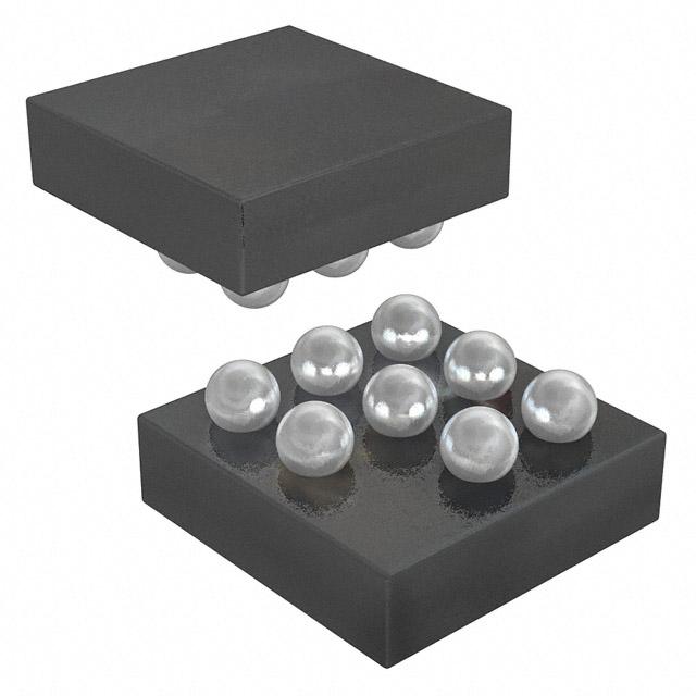
2. Pinning information
2.1 Pinning
bump A1
index area
1
2
3
A
B
C
008aaa206
transparent top view,
solder balls facing down
Fig 1.
Pin configuration
2.2 Pin description
Table 1.
Pinning
Pin
Description
A1
not connected (missing ball)
A2
external pin 1
A3
internal pin 1
B1
external pin 2
B2
ground
B3
internal pin 2
C1
external pin 3
C2
supply ESD protection
C3
internal pin 3
3. Ordering information
Table 2.
Ordering information
Type number
Package
Name
Description
Version
IP4064CX8/LF/P
WLCSP8
wafer level chip-size package; 8 bumps; 1.41 × 1.41 × 0.65 mm
IP4064CX8/LF/P
IP4364CX8/LF/P
WLCSP8
wafer level chip-size package; 8 bumps; 1.16 × 1.16 × 0.61 mm
IP4364CX8/LF/P
IP4366CX8/P
WLCSP8
wafer level chip-size package; 8 bumps; 1.16 × 1.16 × 0.61 mm
IP4366CX8/P
IP4064CX8_IP4364CX8_IP4366CX8_2
Product data sheet
All information provided in this document is subject to legal disclaimers.
Rev. 02 — 11 February 2010
© NXP B.V. 2010. All rights reserved.
2 of 14
�IP4064CX8; IP4364CX8; IP4366CX8
NXP Semiconductors
Integrated SIM card passive filter array with ESD protection
4. Functional diagram
C2
R1
A3
100 Ω
A2
R2
B3
47 Ω
B1
R3
C3
IEC61000-4-2
level 1
protection pins
100 Ω
C1
IEC61000-4-2
level 4
protection pins
B2
008aaa210
Fig 2.
Schematic diagram
5. Limiting values
Table 3.
Limiting values
In accordance with the Absolute Maximum Rating System (IEC 60134).
Symbol
Parameter
VI
input voltage
VESD
electrostatic discharge
voltage
Conditions
Min
Max
Unit
−0.5
+5.5
V
pins A2, B1, C1 and C2
to ground
contact discharge
[1]
−15
+15
kV
air discharge
[1]
−15
+15
kV
contact discharge
−8
+8
kV
air discharge
−15
+15
kV
contact discharge
−2
+2
kV
air discharge
−2
+2
kV
IEC 61000-4-2 level 4;
pins A2, B1, C1 and C2
to ground
IEC 61000-4-2 level 1;
pins A3, B3 and C3 to
ground
Pch
channel power dissipation
continuous power;
Tamb = 70 °C
-
60
mW
Ptot
total power dissipation
continuous power;
Tamb = 70 °C
-
180
mW
Tstg
storage temperature
−55
+150
°C
-
260
°C
−35
+85
°C
Treflow(peak) peak reflow temperature
Tamb
[1]
IP4064CX8_IP4364CX8_IP4366CX8_2
Product data sheet
10 s maximum
ambient temperature
Device is qualified with 1000 pulses of ±15 kV contact discharges each, according to the IEC61000-4-2
model and far exceeds the specified level 4 (8 kV contact discharge).
All information provided in this document is subject to legal disclaimers.
Rev. 02 — 11 February 2010
© NXP B.V. 2010. All rights reserved.
3 of 14
�NXP Semiconductors
IP4064CX8; IP4364CX8; IP4366CX8
Integrated SIM card passive filter array with ESD protection
6. Characteristics
Table 4.
Electrical characteristics
Tamb = 25 °C; unless otherwise specified.
Symbol Parameter
Conditions
Min
Typ
Max
Unit
75
100
125
Ω
35.2
47.0
58.8
Ω
IP4064CX8
14
17
20
pF
IP4364CX8
14
17
20
pF
IP4366CX8
8
10
12
pF
Rs(ch)
channel series resistance R1 and R3
Cch
channel capacitance
R2
including diode
capacitance;
Vbias(DC) = 0 V; f = 1 MHz
[1]
VBR
breakdown voltage
Itest = 1 mA
6
-
10
V
ILR
reverse leakage current
VI = 3 V
-
-
50
nA
[1]
Guaranteed by design.
7. Application information
7.1 Application diagram
A typical application diagram showing IP4064CX8, IP4364CX8 or IP4366CX8 in a SIM
card interface is depicted in Figure 3. The 2 kV ESD compliant pins (A3, B3 and C3) are
connected to the baseband interface side while the four 15 kV ESD compliant pins (A2,
B1, C1 and C2) are connected to the SIM card.
VSIM
C2
RST
CLK
I/O
R1
A3
A2
100 Ω
R2
B3
B1
47 Ω
R3
C3
100 Ω
baseband
B2
C1
VCC
GND
RST
SPU
CLK
I/O
AUX1 AUX2
SIM card
008aaa211
Fig 3.
IP4064CX8_IP4364CX8_IP4366CX8_2
Product data sheet
Typical application diagram
All information provided in this document is subject to legal disclaimers.
Rev. 02 — 11 February 2010
© NXP B.V. 2010. All rights reserved.
4 of 14
�IP4064CX8; IP4364CX8; IP4366CX8
NXP Semiconductors
Integrated SIM card passive filter array with ESD protection
7.2 Insertion loss
The IP4064CX8, IP4364CX8 and IP4366CX8 are mainly designed as an EMI/RFI filter for
SIM card interfaces. The insertion loss measurement configuration of a typical 50 Ω
NetWork Analyzer (NWA) system for evaluation of the IP4064CX8, IP4364CX8 and
IP4366CX8 is shown in Figure 4.
The insertion loss in a 50 Ω NWA system for all three channels of IP4064CX8 and
IP4364CX8 is depicted in Figure 5a while insertion loss of IP4366CX8 is shown in
Figure 5b. The insertion loss is measured with a test Printed-Circuit Board (PCB) utilizing
laser drilled micro-via holes that connect the PCB ground plane to the ground pins.
IN
DUT
OUT
50 Ω
50 Ω
TEST BOARD
Vgen
001aai755
Fig 4.
Frequency response measurement configuration
001aag219
0
s21
(dB)
008aaa207
0
s21
(dB)
−10
(1)
−10
(1)
−20
−20
(2)
(2)
(3)
(3)
−30
−40
10−1
1
10
102
−30
103
104
f (MHz)
−40
10−1
1
10
102
103
104
f (MHz)
(1) Channel B1 to B3.
(2) Channel A2 to A3.
(3) Channel C1 to C3.
a. IP4064CX8 and IP4364CX8
Fig 5.
b. IP4366CX8
Measured insertion loss magnitudes
IP4064CX8_IP4364CX8_IP4366CX8_2
Product data sheet
All information provided in this document is subject to legal disclaimers.
Rev. 02 — 11 February 2010
© NXP B.V. 2010. All rights reserved.
5 of 14
�NXP Semiconductors
IP4064CX8; IP4364CX8; IP4366CX8
Integrated SIM card passive filter array with ESD protection
7.3 Crosstalk
The crosstalk measurement configuration of a typical 50 Ω NWA system for evaluation of
the IP4064CX8, IP4364CX8 and IP4366CX8 is shown in Figure 6.
Four typical examples of crosstalk measurement results of IP4064CX8 and IP4364CX8
are depicted in Figure 7a. The crosstalk behavior of IP4366CX8 is shown in Figure 7b.
Unused channels are terminated with 50 Ω to ground.
IN_1
50 Ω
DUT
IN_2
50 Ω
OUT_2
OUT_1
TEST BOARD
50 Ω
50 Ω
Vgen
001aai756
Fig 6.
Crosstalk measurement configuration
008aaa208
0
αct
(dB)
αct
(dB)
−20
−20
(1)
(2)
(3)
(4)
−40
−60
−80
−80
1
10
102
(1)
(2)
(3)
(4)
(5)
(6)
−40
−60
−100
008aaa209
0
103
104
−100
1
10
f (MHz)
102
103
104
f (MHz)
(1) Pin C1 to pin B3.
(1) Pin B1 to pin C3.
(2) Pin B1 to pin C3.
(2) Pin A2 to pin B3.
(3) Pin B1 to pin A3.
(3) Pin B1 to pin A3.
(4) Pin A2 to pin C3.
(4) Pin A2 to pin C3.
(5) Pin C2 to pin A3.
(6) Pin C2 to pin C3.
a. IP4064CX8 and IP4364CX8
Fig 7.
b. IP4366CX8
Measured crosstalk between different channels
IP4064CX8_IP4364CX8_IP4366CX8_2
Product data sheet
All information provided in this document is subject to legal disclaimers.
Rev. 02 — 11 February 2010
© NXP B.V. 2010. All rights reserved.
6 of 14
�IP4064CX8; IP4364CX8; IP4366CX8
NXP Semiconductors
Integrated SIM card passive filter array with ESD protection
8. Package outline
WLCSP8: wafer level chip-size package; 8 bumps (3 x 3 - A1)
D
bump A1
index area
A2
E
A
A1
detail X
e1
b
e
C
e
e1
B
A
1
2
3
X
European
projection
wlcsp8_3x3-a1_po
Fig 8.
Package outline (WLCSP8)
IP4064CX8_IP4364CX8_IP4366CX8_2
Product data sheet
All information provided in this document is subject to legal disclaimers.
Rev. 02 — 11 February 2010
© NXP B.V. 2010. All rights reserved.
7 of 14
�NXP Semiconductors
IP4064CX8; IP4364CX8; IP4366CX8
Integrated SIM card passive filter array with ESD protection
Table 5.
Dimensions for Figure 8
Symbol
Min
Typ
Max
Unit
A
0.60
0.65
0.70
mm
A1
0.22
0.24
0.26
mm
A2
0.38
0.41
0.44
mm
b
0.27
0.32
0.37
mm
D
1.36
1.41
1.46
mm
E
1.36
1.41
1.46
mm
e
-
0.5
-
mm
e1
-
1.0
-
mm
A
0.56
0.61
0.66
mm
A1
0.18
0.20
0.22
mm
A2
0.38
0.41
0.44
mm
b
0.21
0.26
0.31
mm
D
1.11
1.16
1.21
mm
E
1.11
1.16
1.21
mm
e
-
0.4
-
mm
e1
-
0.8
-
mm
IP4064CX8
IP4364CX8 and IP4366CX8
IP4064CX8_IP4364CX8_IP4366CX8_2
Product data sheet
All information provided in this document is subject to legal disclaimers.
Rev. 02 — 11 February 2010
© NXP B.V. 2010. All rights reserved.
8 of 14
�NXP Semiconductors
IP4064CX8; IP4364CX8; IP4366CX8
Integrated SIM card passive filter array with ESD protection
9. Soldering of WLCSP packages
9.1 Introduction to soldering WLCSP packages
This text provides a very brief insight into a complex technology. A more in-depth account
of soldering WLCSP (Wafer Level Chip-Size Packages) can be found in application note
AN10439 “Wafer Level Chip Scale Package” and in application note AN10365 “Surface
mount reflow soldering description”.
Wave soldering is not suitable for this package.
All NXP WLCSP packages are lead-free.
9.2 Board mounting
Board mounting of a WLCSP requires several steps:
1. Solder paste printing on the PCB
2. Component placement with a pick and place machine
3. The reflow soldering itself
9.3 Reflow soldering
Key characteristics in reflow soldering are:
• Lead-free versus SnPb soldering; note that a lead-free reflow process usually leads to
higher minimum peak temperatures (see Figure 9) than a PbSn process, thus
reducing the process window
• Solder paste printing issues, such as smearing, release, and adjusting the process
window for a mix of large and small components on one board
• Reflow temperature profile; this profile includes preheat, reflow (in which the board is
heated to the peak temperature), and cooling down. It is imperative that the peak
temperature is high enough for the solder to make reliable solder joints (a solder paste
characteristic) while being low enough that the packages and/or boards are not
damaged. The peak temperature of the package depends on package thickness and
volume and is classified in accordance with Table 6.
Table 6.
Lead-free process (from J-STD-020C)
Package thickness (mm)
Package reflow temperature (°C)
Volume (mm3)
< 350
350 to 2 000
> 2 000
< 1.6
260
260
260
1.6 to 2.5
260
250
245
> 2.5
250
245
245
Moisture sensitivity precautions, as indicated on the packing, must be respected at all
times.
Studies have shown that small packages reach higher temperatures during reflow
soldering, see Figure 9.
IP4064CX8_IP4364CX8_IP4366CX8_2
Product data sheet
All information provided in this document is subject to legal disclaimers.
Rev. 02 — 11 February 2010
© NXP B.V. 2010. All rights reserved.
9 of 14
�IP4064CX8; IP4364CX8; IP4366CX8
NXP Semiconductors
Integrated SIM card passive filter array with ESD protection
maximum peak temperature
= MSL limit, damage level
temperature
minimum peak temperature
= minimum soldering temperature
peak
temperature
time
001aac844
MSL: Moisture Sensitivity Level
Fig 9.
Temperature profiles for large and small components
For further information on temperature profiles, refer to application note AN10365
“Surface mount reflow soldering description”.
9.3.1 Stand off
The stand off between the substrate and the chip is determined by:
• The amount of printed solder on the substrate
• The size of the solder land on the substrate
• The bump height on the chip
The higher the stand off, the better the stresses are released due to TEC (Thermal
Expansion Coefficient) differences between substrate and chip.
9.3.2 Quality of solder joint
A flip-chip joint is considered to be a good joint when the entire solder land has been
wetted by the solder from the bump. The surface of the joint should be smooth and the
shape symmetrical. The soldered joints on a chip should be uniform. Voids in the bumps
after reflow can occur during the reflow process in bumps with high ratio of bump diameter
to bump height, i.e. low bumps with large diameter. No failures have been found to be
related to these voids. Solder joint inspection after reflow can be done with X-ray to
monitor defects such as bridging, open circuits and voids.
9.3.3 Rework
In general, rework is not recommended. By rework we mean the process of removing the
chip from the substrate and replacing it with a new chip. If a chip is removed from the
substrate, most solder balls of the chip will be damaged. In that case it is recommended
not to re-use the chip again.
IP4064CX8_IP4364CX8_IP4366CX8_2
Product data sheet
All information provided in this document is subject to legal disclaimers.
Rev. 02 — 11 February 2010
© NXP B.V. 2010. All rights reserved.
10 of 14
�IP4064CX8; IP4364CX8; IP4366CX8
NXP Semiconductors
Integrated SIM card passive filter array with ESD protection
Device removal can be done when the substrate is heated until it is certain that all solder
joints are molten. The chip can then be carefully removed from the substrate without
damaging the tracks and solder lands on the substrate. Removing the device must be
done using plastic tweezers, because metal tweezers can damage the silicon. The
surface of the substrate should be carefully cleaned and all solder and flux residues
and/or underfill removed. When a new chip is placed on the substrate, use the flux
process instead of solder on the solder lands. Apply flux on the bumps at the chip side as
well as on the solder pads on the substrate. Place and align the new chip while viewing
with a microscope. To reflow the solder, use the solder profile shown in application note
AN10365 “Surface mount reflow soldering description”.
9.3.4 Cleaning
Cleaning can be done after reflow soldering.
10. Abbreviations
Table 7.
Abbreviations
Acronym
Description
DUT
Device Under Test
EMI
ElectroMagnetic Interference
ESD
ElectroStatic Discharge
NWA
NetWork Analyzer
PCB
Printed-Circuit Board
PCS
Personal Communication System
RFI
Radio Frequency Interference
RoHS
Restriction of Hazardous Substances
SIM
Subscriber Identity Module
WLCSP
Wafer-Level Chip-Scale Package
11. Revision history
Table 8.
Revision history
Document ID
Release date
Data sheet status Change notice Supersedes
IP4064CX8_IP4364CX8_
IP4366CX8_2
20100211
Product data sheet -
Modifications:
•
•
•
Type number IP4366CX8 added
Figure 3: added
General editorial update
IP4064CX8LF_IP4364CX8LF_1 20071112
IP4064CX8_IP4364CX8_IP4366CX8_2
Product data sheet
IP4064CX8LF_IP4364CX8LF_1
Product data sheet -
All information provided in this document is subject to legal disclaimers.
Rev. 02 — 11 February 2010
-
© NXP B.V. 2010. All rights reserved.
11 of 14
�NXP Semiconductors
IP4064CX8; IP4364CX8; IP4366CX8
Integrated SIM card passive filter array with ESD protection
12. Legal information
12.1 Data sheet status
Document status[1][2]
Product status[3]
Definition
Objective [short] data sheet
Development
This document contains data from the objective specification for product development.
Preliminary [short] data sheet
Qualification
This document contains data from the preliminary specification.
Product [short] data sheet
Production
This document contains the product specification.
[1]
Please consult the most recently issued document before initiating or completing a design.
[2]
The term ‘short data sheet’ is explained in section “Definitions”.
[3]
The product status of device(s) described in this document may have changed since this document was published and may differ in case of multiple devices. The latest product status
information is available on the Internet at URL http://www.nxp.com.
12.2 Definitions
Draft — The document is a draft version only. The content is still under
internal review and subject to formal approval, which may result in
modifications or additions. NXP Semiconductors does not give any
representations or warranties as to the accuracy or completeness of
information included herein and shall have no liability for the consequences of
use of such information.
Short data sheet — A short data sheet is an extract from a full data sheet
with the same product type number(s) and title. A short data sheet is intended
for quick reference only and should not be relied upon to contain detailed and
full information. For detailed and full information see the relevant full data
sheet, which is available on request via the local NXP Semiconductors sales
office. In case of any inconsistency or conflict with the short data sheet, the
full data sheet shall prevail.
Product specification — The information and data provided in a Product
data sheet shall define the specification of the product as agreed between
NXP Semiconductors and its customer, unless NXP Semiconductors and
customer have explicitly agreed otherwise in writing. In no event however,
shall an agreement be valid in which the NXP Semiconductors product is
deemed to offer functions and qualities beyond those described in the
Product data sheet.
12.3 Disclaimers
Limited warranty and liability — Information in this document is believed to
be accurate and reliable. However, NXP Semiconductors does not give any
representations or warranties, expressed or implied, as to the accuracy or
completeness of such information and shall have no liability for the
consequences of use of such information.
In no event shall NXP Semiconductors be liable for any indirect, incidental,
punitive, special or consequential damages (including - without limitation - lost
profits, lost savings, business interruption, costs related to the removal or
replacement of any products or rework charges) whether or not such
damages are based on tort (including negligence), warranty, breach of
contract or any other legal theory.
Notwithstanding any damages that customer might incur for any reason
whatsoever, NXP Semiconductors’ aggregate and cumulative liability towards
customer for the products described herein shall be limited in accordance
with the Terms and conditions of commercial sale of NXP Semiconductors.
malfunction of an NXP Semiconductors product can reasonably be expected
to result in personal injury, death or severe property or environmental
damage. NXP Semiconductors accepts no liability for inclusion and/or use of
NXP Semiconductors products in such equipment or applications and
therefore such inclusion and/or use is at the customer’s own risk.
Applications — Applications that are described herein for any of these
products are for illustrative purposes only. NXP Semiconductors makes no
representation or warranty that such applications will be suitable for the
specified use without further testing or modification.
NXP Semiconductors does not accept any liability related to any default,
damage, costs or problem which is based on a weakness or default in the
customer application/use or the application/use of customer’s third party
customer(s) (hereinafter both referred to as “Application”). It is customer’s
sole responsibility to check whether the NXP Semiconductors product is
suitable and fit for the Application planned. Customer has to do all necessary
testing for the Application in order to avoid a default of the Application and the
product. NXP Semiconductors does not accept any liability in this respect.
Limiting values — Stress above one or more limiting values (as defined in
the Absolute Maximum Ratings System of IEC 60134) will cause permanent
damage to the device. Limiting values are stress ratings only and (proper)
operation of the device at these or any other conditions above those given in
the Recommended operating conditions section (if present) or the
Characteristics sections of this document is not warranted. Constant or
repeated exposure to limiting values will permanently and irreversibly affect
the quality and reliability of the device.
Terms and conditions of commercial sale — NXP Semiconductors
products are sold subject to the general terms and conditions of commercial
sale, as published at http://www.nxp.com/profile/terms, unless otherwise
agreed in a valid written individual agreement. In case an individual
agreement is concluded only the terms and conditions of the respective
agreement shall apply. NXP Semiconductors hereby expressly objects to
applying the customer’s general terms and conditions with regard to the
purchase of NXP Semiconductors products by customer.
No offer to sell or license — Nothing in this document may be interpreted or
construed as an offer to sell products that is open for acceptance or the grant,
conveyance or implication of any license under any copyrights, patents or
other industrial or intellectual property rights.
Export control — This document as well as the item(s) described herein
may be subject to export control regulations. Export might require a prior
authorization from national authorities.
Right to make changes — NXP Semiconductors reserves the right to make
changes to information published in this document, including without
limitation specifications and product descriptions, at any time and without
notice. This document supersedes and replaces all information supplied prior
to the publication hereof.
Non-automotive qualified products — Unless the data sheet of an NXP
Semiconductors product expressly states that the product is automotive
qualified, the product is not suitable for automotive use. It is neither qualified
nor tested in accordance with automotive testing or application requirements.
NXP Semiconductors accepts no liability for inclusion and/or use of
non-automotive qualified products in automotive equipment or applications.
Suitability for use — NXP Semiconductors products are not designed,
authorized or warranted to be suitable for use in medical, military, aircraft,
space or life support equipment, nor in applications where failure or
In the event that customer uses the product for design-in and use in
automotive applications to automotive specifications and standards, customer
(a) shall use the product without NXP Semiconductors’ warranty of the
IP4064CX8_IP4364CX8_IP4366CX8_2
Product data sheet
All information provided in this document is subject to legal disclaimers.
Rev. 02 — 11 February 2010
© NXP B.V. 2010. All rights reserved.
12 of 14
�NXP Semiconductors
IP4064CX8; IP4364CX8; IP4366CX8
Integrated SIM card passive filter array with ESD protection
product for such automotive applications, use and specifications, and (b)
whenever customer uses the product for automotive applications beyond
NXP Semiconductors’ specifications such use shall be solely at customer’s
own risk, and (c) customer fully indemnifies NXP Semiconductors for any
liability, damages or failed product claims resulting from customer design and
use of the product for automotive applications beyond NXP Semiconductors’
standard warranty and NXP Semiconductors’ product specifications.
12.4 Trademarks
Notice: All referenced brands, product names, service names and trademarks
are the property of their respective owners.
13. Contact information
For more information, please visit: http://www.nxp.com
For sales office addresses, please send an email to: salesaddresses@nxp.com
IP4064CX8_IP4364CX8_IP4366CX8_2
Product data sheet
All information provided in this document is subject to legal disclaimers.
Rev. 02 — 11 February 2010
© NXP B.V. 2010. All rights reserved.
13 of 14
�NXP Semiconductors
IP4064CX8; IP4364CX8; IP4366CX8
Integrated SIM card passive filter array with ESD protection
14. Contents
1
1.1
1.2
1.3
2
2.1
2.2
3
4
5
6
7
7.1
7.2
7.3
8
9
9.1
9.2
9.3
9.3.1
9.3.2
9.3.3
9.3.4
10
11
12
12.1
12.2
12.3
12.4
13
14
Product profile . . . . . . . . . . . . . . . . . . . . . . . . . . 1
General description . . . . . . . . . . . . . . . . . . . . . 1
Features and benefits . . . . . . . . . . . . . . . . . . . . 1
Applications . . . . . . . . . . . . . . . . . . . . . . . . . . . 1
Pinning information . . . . . . . . . . . . . . . . . . . . . . 2
Pinning . . . . . . . . . . . . . . . . . . . . . . . . . . . . . . . 2
Pin description . . . . . . . . . . . . . . . . . . . . . . . . . 2
Ordering information . . . . . . . . . . . . . . . . . . . . . 2
Functional diagram . . . . . . . . . . . . . . . . . . . . . . 3
Limiting values. . . . . . . . . . . . . . . . . . . . . . . . . . 3
Characteristics . . . . . . . . . . . . . . . . . . . . . . . . . . 4
Application information. . . . . . . . . . . . . . . . . . . 4
Application diagram . . . . . . . . . . . . . . . . . . . . . 4
Insertion loss . . . . . . . . . . . . . . . . . . . . . . . . . . 5
Crosstalk. . . . . . . . . . . . . . . . . . . . . . . . . . . . . . 6
Package outline . . . . . . . . . . . . . . . . . . . . . . . . . 7
Soldering of WLCSP packages. . . . . . . . . . . . . 9
Introduction to soldering WLCSP packages . . . 9
Board mounting . . . . . . . . . . . . . . . . . . . . . . . . 9
Reflow soldering . . . . . . . . . . . . . . . . . . . . . . . . 9
Stand off . . . . . . . . . . . . . . . . . . . . . . . . . . . . . 10
Quality of solder joint . . . . . . . . . . . . . . . . . . . 10
Rework . . . . . . . . . . . . . . . . . . . . . . . . . . . . . . 10
Cleaning . . . . . . . . . . . . . . . . . . . . . . . . . . . . . 11
Abbreviations . . . . . . . . . . . . . . . . . . . . . . . . . . 11
Revision history . . . . . . . . . . . . . . . . . . . . . . . . 11
Legal information. . . . . . . . . . . . . . . . . . . . . . . 12
Data sheet status . . . . . . . . . . . . . . . . . . . . . . 12
Definitions . . . . . . . . . . . . . . . . . . . . . . . . . . . . 12
Disclaimers . . . . . . . . . . . . . . . . . . . . . . . . . . . 12
Trademarks. . . . . . . . . . . . . . . . . . . . . . . . . . . 13
Contact information. . . . . . . . . . . . . . . . . . . . . 13
Contents . . . . . . . . . . . . . . . . . . . . . . . . . . . . . . 14
Please be aware that important notices concerning this document and the product(s)
described herein, have been included in section ‘Legal information’.
© NXP B.V. 2010.
All rights reserved.
For more information, please visit: http://www.nxp.com
For sales office addresses, please send an email to: salesaddresses@nxp.com
Date of release: 11 February 2010
Document identifier: IP4064CX8_IP4364CX8_IP4366CX8_2
�