D~5C-c::t\ +~VI u ~
,.
+5VPowered
ANALOG
W DEVICES
CMOSRS-232Drivers/Receivers
FEATURES
Single 5 V Power Supply
Meets All RS-232-C and V.28 Specifications
Multiple Drivers and Receivers
On-Board DC-DC Converters
:t:9 V Output Swing with +5 V Supply
low Power CMOS: 5 mA Operation
low Power Shutdown $1 p.A
3-State TTl/CMOS Receiver Outputs
:t:30 V Receiver Input levels
Plug-In Replacement for MAX230-241
OBS
APPLICATIONS
Computers
Peripherals
Modems
Printers
Instruments
OLE
GENERAL DESCRIPTION
The AD230 family of 5 V only, RS-232 line drivers/receivers
provides a variety of configurations to fit most communication
needs, especially in applications where :t 12 V is not available.
The AD230, AD235, AD236 and AD241 feature a low power
shutdown mode which reduces power dissipation to less than
5 j.L
W making them ideally suited for battery powered equipment. The AD233 and AD235 do not require any external components and are particularly useful in applications where printed
circuit board space is critical.
SELECTION
Part
Number
AD230
AD231
AD232
AD233
AD234
AD235
AD236
AD237
AD238
AD239
AD241
1\ll members of the AD230 family, except the AD231 and the
AD239, include tWointernal charge pump voltage converters
which allow operation from a single +5 V supply. These converters convert the + 5 V input power to the :t 10 V required for
RS-232 output levels. The AD231 and AD239 are designed to
operate from +5 V and + 12 V supplies. An internal + 12 V to
- 12 V charge pump voltage converter generates the - 12 V
supply.
TE
In order to minimize the package count in all applications, a
wide selection of driver/receiver combinations is available (see
table below).
TABLE
Power
Supply Voltage
+5 V
+5 V & +7.5 V
to 13.2V
+5 V
+5 V
+5 V
+5 V
+5 V
+5 V
+5 V
+5 V & +12 V
+5 V
Low Power
Shutdown
(SD)
Yes
No
TTL
Three-State
EN
No. of
Pins
0
2
External
Capacitors
4
2
No
No
20
14
2
2
0
5
3
3
4
5
5
4
None
4
None
4
4
4
2
4
No
No
No
Yes
Yes
No
No
No
Yes
No
No
No
Yes
Yes
No
No
Yes
Yes
16
20
16
24
24
24
24
24
28
No. of
RS-232
Drivers
No. of
RS-232
Receivers
5
2
2
2
4
5
4
5
4
3
4
Information furnished by Analog Devices is believed to be accurate and
reliable. However, no responsibility is assumed by Analog Devices for its
use; nor for any infringements of patents or other rights of third parties
which may result from its use. No license is granted by implication or
otherwise under any patent or patent rights of Analog Devices.
"
One Technology Way, P.O. Box 9106, Norwood, MA 02062-9106, U.S.A.
Tel: 617/329-4700
Fax: 617/326-8703
Twx: 710/394-6577
Telex: 924491
Cable: ANALOG NORWOODMASS
�V :t 10% (AD231,AD232,AD234,AD236,AD238,AD239,AD241);Vee = +5 V :t 5% (AD233,
= 7.5Vto 13.2V (AD231)&V+ = 12 V :t 10% (AD239);All Specifications Tminto Tmax
unlessotherwise
noted.)
= +5
(Vee
AD235);V+
SPECIFICATIONS
Parameter
Min
Output Voltage Swing
Vcc Power Supply Current
::I::5
V+ Power Supply Current
Shutdown Supply Current
Input Logic Threshold Low, VINL
Input Logic Threshold High, VINH
Logic Pullup Current
15
-30
0.8
0.2
3
1.2
1.7
0.5
5
2.4
1.0
7
0.4
3.5
0.05
400
250
Propagation Delay
Instantaneous Slew Ratel
Transition Region Slew Rate
0.5
NOTE
tested to ensure compliance.
notice.
300
Test Conditions/Comments
Volts
mA
mA
mA
f.LA
V
V
f.LA
V
V
V
V
kil
V
V
All Transmitter Outputs Loaded with 3 kil to Ground
No Load, T A = 25°C
AD231, AD239
No Load, V+ = 12 V AD231 & AD239 Only
30
TIN
= 0V
Vcc = 5 V, TA = +25°C
Vcc = 5 V, TA = +25°C
Vcc=5V
Vcc = 5V, TA = +25°C
lOUT
= 3.2 mA
lOUT
=
-1.0
mA
TE
::1::10
Power Dissipation
Cerdip (Derate 9.5 mW/OCabove +70°C)
Plastic DIP (Derate 7 mW/OCabove +70°C)
SOIC (Derate 7 mW/oC above +70°C)
Operating Temperature Range
Commercial (J Version)
(T A = 25°C unless otherwise noted)
0.3Vto+6V
(Vcc-0.3V)to+13V
+0.3Vto-13V
::I::30V
0 to +70°C
-55°C to + 125ac
Extended (S Version) """""""
Storage Temperature Range.
. . . . . . . . . . -65ac to + 150ac
Lead Temperature (Soldering, 10 secs) . . . . . . . . . . . + 300°C
O.3Vto(Vcc+O.3V)
*This is a stress rating only and functional operation of the device
at these or any other conditions above those indicated in the
operation sections of this specification is not implied. Exposure
to absolute maximum rating conditions for extended periods of
time may affect reliability.
Continuous
CAUTION
ESD (electrostatic discharge) sensitive device. The digital control inputs are diode protected;
however, permanent damage may occur on unconnected devices subject to high energy electrostatic fields. Unused devices must be stored in conductive foam or shunts. The protective foam
should be discharged to the destination socket before devices are removed.
-2~---
675 mW
375 mW
375 mW
Industrial (A Version) . . . . . . . . . . . . . . . -40°C to +85°C
0.3Vto(Vcc+0.3V)
TOUT' . . . . . . . . . . . . . . (V+, +0.3 V) to (V-, -0.3 V)
ROUT
Short Circuit Duration
TOUT
= +25°C
EN = Vceo0 V ::; ROUT::;Vcc
AD235, AD236, AD239, AD241
(Figure 25. RL = 1 kil, CL = 150 pF)
ns
AD235, AD236, AD239, AD241
(Figure 25. RL = 1 kil, CL = 150 pF)
RS-232 to TTL
f.Ls
V/f.LS CL = 10pF, RL = 3-7 kil, TA = +25°C
V/f.LS RL = 3 kil, CL = 2500pF
Measured from +3 V to -3 V or -3 V to +3 V
il
Vcc = V+ = V- = 0 V, VOUT = ::1::2
V
mA
ABSOLUTE MAXIMUM RATINGS*
Vcc
V+
VInput Voltages
TIN
R1N
Output Voltages
TA
TIN' EN, SD
TIN' EN, SD
::1::10 f.LA
ns
3
Output Resistance
RS-232 Output Short Circuit Current
Units
OLE
Output Disable Time (Tod
subject to change without
200
+30
OBS
'Sample
10
1
10
10
0.8
2.0
RS-232 Input Voltage Range
RS-232 Input Threshold Low
RS-232 Input Threshold High
RS-232 Input Hysteresis
RS-232 Input Resistance
TTL/CMOS Output Voltage Low, VOL
TTL/CMOS Output Voltage High, VOH
TTL/CMOS Output Leakage Current
Output Enable Time (TEN)
Specifications
Max
Typ
::I::9
4
0.4
5
1
-
�)
10l-lF
T30UT
I+ 16V
T10UT
T21N
T21N
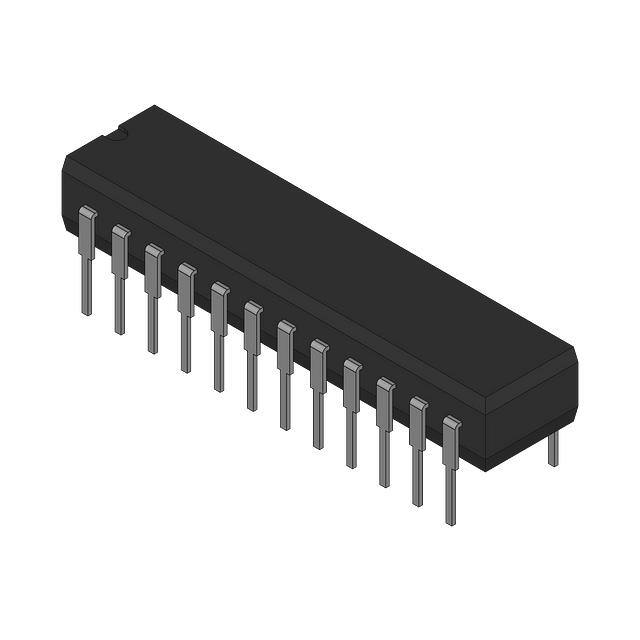
AD230
TOP VIEW
(Not to Scale)
T1IN
GND
OBS
INPUTS*
Vcc
TTL/CMOS
C1+
)
i
4
3
14
1
T1oUT
T2oUT
2"
T31N
T30UT
OUTPUTS
20
15
T41N
T4oUT
V+
NC
= NO
19
16
18
17
OLE
CONNECT
T5'N
NC
T50UT
AD230
-
-
TE
"INTERNAL 400kfl PULL.UP RESISTORON EACH TTLiCMOS INPUT
Figure 2. AD230 Typical Operating
)
DIP
)
C+
T10UT
A1oUT
T21N
T11N
C+
C-
.
T11N
TTLICMOS
INPUTS*
{
SOIC
T21N
R10UT
TTL/CMOS
OUTPUTS
V-
+12V TO -12V
1N914 OR EQUIVALENT
V+
4.71-lF
VOLTAGE
CONVERTER
v-h
CI+16V
81
1_'-...111
71
91
61
{
Circuit
I..T
Vcc
AD231
TOP VIEW
(Not to Scale)
,
SD
GND
6
Figure 1. AD230 DIP/SOIC Pin Configuration
I_-
14
110
_"""':-1
_./
I
..
.
15
R2oUT
AD231
TOP VIEW
T20UT
A21N
(Not to Scale)
RS-232
OUTPUTS
T2oUT
T1.
--
R21N
AD231
GND
II!!! A11N
12
"INTERNAL 400kfl PULL.UP RESISTORON EACH TTL/CMOS INPUT
**INTERNAL 5kfl PULL.DOWN RESISTORON EACH RS.232 INPUT
T21N
NC
NC
= NO
Figure 4. AD231 Typical Operating Circuit
CONNECT
Figure 3. AD231 DIP & SOIC Pin Configurations
-3-
}
RS-232
INPUTS**
RI'"}
A2oUT
)
.
12
T1INT
T20UT
�+5VINPUT
10".F...L+
6.3VI
16
1 '(;1+
Vcc
+5V TO +10V
2
3Ic1-VOLTAGE
DOUBLERV+
6
41C2+
+10V TO -10V
VC2-VOLTAGEINVERTER
5
AD232
TOP VIEW
(Not to Scale)
1_"'-
114
10".F
~+
16:0"'
TTL/CMOS
INPUTS'
{
OBS
T2'N1
{
17
_/.I
113
__I
18
}
R2oUT-
91
R1'N
R2'N
I
RI,
-
RS-232
OUTPUTS
T2oUT
T1,"1
TTL/CMOS
OUTPUTS
Figure 5. AD232 DIP/SOIC Pin Configuration
1_"'-
}
RS-232
INPUTS"
OLE
AD232
GND
15
-
'INTERNAL 400kil PULL-UP RESISTORON EACH TTLiCMOS INPUT
**INTERNAL 5kil PULL-DOWN RESISTORON EACH RS-232 INPUT
TE
Figure 6. AD232 Typical Operating Circuit
+5VINPUT
7
Vcc
{
R1oUT
T1oUT
18
T2'N
3
R11N
GND
5
TTL/CMOS
INPUTS'
T11N
T1oUT
2
n'N
T21N
(Not to Scale)
TTL/CMOS
OUTPUTS
{
}
R1'N
RS-232
INPUTS"
20
19
R2oUT -
8
VCC
DO NOT MAKE
C1+
CONNECTIONS TO
THESE PINS
GND
T2oUT
4
R10UT
AD233
TOPVIEW
RS-232
OUTPUTS
{
C1+
C2+
~C1-
R2'N
11
C2+ 15
INTERNAL
-10V POWER
SUPPLY
{
121V17
V-
INTERNAL
+10V POWER
SUPPLY
14. V+
AD233
C2-
~
10
C2- .16
~
2,ND
6
9
-
Figure 7. AD233 DIP Pin Configuration
'INTERNAL 4O0kil PULL-UP RESISTORON EACH TTLiCMOS INPUT
"INTERNAL 5kil PULL-DOWN RESISTORON EACH RS-232 INPUT
Figure 8. AD233 Typical Operating Circuit
-4~-
---
}
�+5VINPUT
J
7.
6
Vcc
C1+
+5V TO +10V
8
9Ic1-VOLTAGE
DOUBLER V+
12
101C2+ +10V TO -10V
VC2-VOLTAGE INVERTER
T10UT
T2oUT
10l1F
~+16V
4
T21N
T1'N
AD234
TOP VIEW
(Not to Scale)
T11N
GND
3
T2'N
Vcc
OBS
TTL/CMOS
INPUTS*
RS-232
OUTPUTS
13
T3'N
C1-
)
2
T20UT
i
C1+
V+
T10UT
T4'N
16
T30UT
.
141
I
OLE
Figure 9. AD234 DIP/SOIC Pin Configuration
)
.
P5
T40UT
AD234
GND
~
-
'INTERNAL 400kfi PULL-UP RESISTORON EACH TTL/CMOS INPUT
Figure
TE
10. AD234 Typical Operating
Circuit
+5VINPUT
12
v:
T1'N
8
3
T10UT
T20N
7
4
T2oUT
15
2
T4oUT
T30UT
\
)
T10UT
TIL/CMOS
T2 OUT
INPUTS'
~
I
T3'N
R21N
AD235
R2
15'N
T~:
TOP VIEW
T21N
7
T30UT
:~
15
R1oUT
1
9
10
R1'N
R2oUT
6
5
R2'N
23
Figure 11. AD235 DIP Pin Configuration
24
R3oUT
R4oUT
17
18
14
13
R4.N
R5'N
~
~
SD
GND
)
~11
'INTERNAL4OOkU PUll-UP RESISTOR ON EACH TTlfCMOS INPUT
"INTERNAl
SkU PUll-DOWN
RESISTOR ON EACH RS-232 INPUT
Figure 12. AD235 Typical Operating
-5-
~
I
RS-232
R3'N
R5oUT
EN
OUTPUTS
~T~
R1ouT
I
TIL/CMOS
OUTPUTS
RS-232
r
15ouT
AD235
(Not to Scale)
T1IN
I
Circuit
INPUTS"
�T30UT 11 I .
10".F
T10UT
*+16V
T2oUT
2
T1'N
T10UT
R1'N
1
TJON
TOP VIEW
(Notto
Scale)
AD235
T30uT
AD236
19
DIP/SOIC
Pin
Configuration
24
T4
T4'N
5
OBS
13. AD236
RS-232
OUTPUTS
18
Vcc
Figure
3
T2ouT
1
TTL/CMOS
INPUTS'
T11N 7
T2";
GND
6
T2'N
R1oUT
T4oUT
4
R1
R1oUT
R1'N
22
OUTPUTS
TTL/CMOS1
23
R2'N
R2oUT
17
I
16
R30UT
RS-232
R30N
OLE
20
EN
INPUTS'
21
SD
GND
-4-8
'INTERNAL400kH PUll.UP RESISTORON EACHTTl/CMOS INPUT
uiNTERNAl5kH PUll.DOWN RESISTORON EACHRS.232 INPUT
TE
Figure 14. AD236 Typical Operating Circuit
10
~
C1+
121C1-
Vcc
10".F
T-+
vo~i:G~OD~0°~lER
V+ 11
131C2+
+10VTO-10V
VC2- VOLTAGE INVERTER
14 -
T30UT
T1oUT
T1'N-
T2oUT
R11N
T2'N-
6.3V
15
10".F
J::+16V
7
2
6
3
T10UT
R1oUT
T21N
T11N
AD237
TOP VIEW
(Not to Scale)
INPUTS'
i
"-.
18
TJON-
T30UT
AD237
TTLICMOS
19
T4'N-
24
GND
21
T5'N-
Vcc
"'.,'
OUTPUTS
20
T4ouT
T50UT
:
4
R1oUT..--2.
OUTPUTS
TTLICMOS
22
i
23
15. AD237
DIP/SOIC
R2oN
R2oUT-
17
16
R30UT
Figure
R1'N
R:lIN
Pin Configuration
-
GND
-=
8
'INTERNAl400kU
PUll-UP RESISTOR ON EACH TTl/CMOS INPU-;
ulNTERNAl 5kU PUll-DOWN RESISTOR ON EACH RS-232 INPUT
Figure
-6-
16. AD237
Typical
Operating
Circuit
"m
INPUTS"
�}
T2oUT
10f.'F
*+16V
nOUT
2
R2'N
R2oUT
T10UT
T20UT
n'N
24
R1oUT
AD238
R11N
TOP VIEW
(Not to Scale)
I
RS-232
OUTPUTS
T30UT
AD238
20
OBS
T4ouT
GND
R1'N
Vcc
)
R2'N
RS-232
INPUTS"
R3'N
16
R4'N
GND
---e
=
'INTERNAL
"INTERNAl
Figure
)
,
23
OLE
Figure 17, AD238 DIP/SOIC Pin Configuration
,
400k1l PUll.UP
5k1l PUll-DOWN
18. AD238
TE
RESISTOR ON EACH TTliCMOS
INPUT
RESISTOR ON EACH RS.232 INPUT
Typical Operating Circuit
+12V:10%
1N914
OR
EQUIVALENT
10f.'F
R1oUT
R1'N
)
n'N
n
nOUT
GND
TTL/CMOS
INPUTS.
VCC
V+
C+
{'
AD239
TOP VIEW
(Not to Scale)
23
T2'NT20UT
--;--4
TJ'N
R1oUT.
V-
R2oUT
R5'N
OUTPUTS
TTLiCMOS
J
"I
20
T3
RS-232
OUTPUT!>
T30UT
AD239
O


 工商网监
湘ICP备2023018690号
工商网监
湘ICP备2023018690号
