Product
Folder
Order
Now
Support &
Community
Tools &
Software
Technical
Documents
Reference
Design
ADS8528, ADS8548, ADS8568
SBAS543C – AUGUST 2011 – REVISED FEBRUARY 2016
ADS85x8 12-, 14-, and 16-Bit, 8-Channel, Simultaneous Sampling ADCs
1 Features
3 Description
•
The ADS85x8 contain eight low-power, 12-, 14-, or
16-bit, successive approximation register (SAR)based analog-to-digital converters (ADCs) with true
bipolar inputs. These channels are grouped in four
pairs, thus allowing simultaneous high-speed signal
acquisition of up to 650 kSPS.
1
•
•
•
•
•
•
Family of 12-, 14-, and 16-Bit, Pin- and SoftwareCompatible ADCs
Maximum Data Rate per Channel:
– ADS8528: 650 kSPS (PAR) or
480 kSPS (SER)
– ADS8548: 600 kSPS (PAR) or
450 kSPS (SER)
– ADS8568: 510 kSPS (PAR) or
400 kSPS (SER)
Excellent AC Performance:
– Signal-to-Noise Ratio:
ADS8528: 73.9 dB, ADS8548: 85 dB,
ADS8568: 91.5 dB
– Total Harmonic Distortion:
ADS8528: –89 dB, ADS8548: –91 dB,
ADS8568: –94 dB
Programmable, Buffered Internal Reference:
0.5 V–2.5 V or 0.5 V–3.0 V Supports Input
Voltage Ranges up to ±12 V
Selectable Parallel or Serial Interface
Scalable Low-Power Operation Using Auto-Sleep
Mode: Only 32 mW at 10 kSPS
Fully Specified Over Extended Industrial
Temperature Range
The devices support selectable parallel or serial
interface
with
daisy-chain
capability.
The
programmable reference allows handling of analog
input signals with amplitudes up to ±12 V.
The ADS85x8 family supports an auto-sleep mode for
minimum power dissipation and is available in both
64-pin VQFN and LQFP packages. The entire family
is specified over a temperature range of –40°C to
+125°C.
Device Information(1)
PART NUMBER
ADS85x8
PACKAGE
BODY SIZE (NOM)
VQFN (64)
9.00 mm × 9.00 mm
LQFP (64)
10.00 mm × 10.00 mm
(1) For all available packages, see the orderable addendum at
the end of the data sheet.
Simplified Block Diagram
Clock
Generator
2 Applications
•
•
•
•
•
Protection Relays
Power Quality Measurement
Multi-Axis Motor Controls
Programmable Logic Controllers
Industrial Data Acquisition
CH_A0
SAR ADC
CH_A1
SAR ADC
CH_B0
SAR ADC
CH_B1
SAR ADC
Signal-to-Noise Ratio (dB)
SNR vs Temperature
94
92
90
88
86
84
82
80
78
76
74
72
70
−40 −25 −10
ADS8568
ADS8548
ADS8528
5
20 35 50 65
Temperature (°C)
80
95
CH_C0
SAR ADC
CH_C1
SAR ADC
CH_D0
SAR ADC
CH_D1
SAR ADC
REFIO
String DAC
Control
Logic
Control
Signal
Bus
Config
Register
I/O
Parallel
or Serial
Data Bus
2.5-V, 3-V
Reference
110 125
G016
1
An IMPORTANT NOTICE at the end of this data sheet addresses availability, warranty, changes, use in safety-critical applications,
intellectual property matters and other important disclaimers. PRODUCTION DATA.
�ADS8528, ADS8548, ADS8568
SBAS543C – AUGUST 2011 – REVISED FEBRUARY 2016
www.ti.com
Table of Contents
1
2
3
4
5
6
7
Features ..................................................................
Applications ...........................................................
Description .............................................................
Revision History.....................................................
Device Comparison Table.....................................
Pin Configuration and Functions .........................
Specifications.........................................................
1
1
1
2
4
4
9
7.1
7.2
7.3
7.4
7.5
7.6
7.7
7.8
7.9
7.10
Absolute Maximum Ratings ...................................... 9
ESD Ratings.............................................................. 9
Recommended Operating Conditions....................... 9
Thermal Information .................................................. 9
Electrical Characteristics: General .......................... 10
Electrical Characteristics: ADS8528 ....................... 13
Electrical Characteristics: ADS8548 ....................... 14
Electrical Characteristics: ADS8568 ....................... 15
Serial Interface Timing Requirements..................... 16
Parallel Interface Timing Requirements (Read
Access) .................................................................... 17
7.11 Parallel Interface Timing Requirements (Write
Access) .................................................................... 17
7.12 Typical Characteristics .......................................... 20
8
Parameter Measurement information ................ 26
9
Detailed Description ............................................ 26
9.1
9.2
9.3
9.4
9.5
Overview .................................................................
Functional Block Diagram .......................................
Feature Description.................................................
Device Functional Modes........................................
Register Maps ........................................................
26
27
28
34
39
10 Application and Implementation........................ 41
10.1 Application Information.......................................... 41
10.2 Typical Application ................................................ 41
11 Power Supply Recommendations ..................... 46
12 Layout................................................................... 46
12.1 Layout Guidelines ................................................. 46
12.2 Layout Example .................................................... 47
13 Device and Documentation Support ................. 48
13.1
13.2
13.3
13.4
13.5
13.6
Documentation Support .......................................
Related Links ........................................................
Community Resources..........................................
Trademarks ...........................................................
Electrostatic Discharge Caution ............................
Glossary ................................................................
48
48
48
48
48
48
14 Mechanical, Packaging, and Orderable
Information ........................................................... 48
8.1 Equivalent Circuits .................................................. 26
4 Revision History
NOTE: Page numbers for previous revisions may differ from page numbers in the current version.
Changes from Revision B (November 2015) to Revision C
•
Page
Changed Figure 45: changed capacitor values from 820 nF to 820 pF .............................................................................. 42
Changes from Revision A (October 2011) to Revision B
Page
•
Added ESD Ratings table, Recommended Operating Conditions table, Feature Description section, Device
Functional Modes section, Register Maps section, Application and Implementation section, Power Supply
Recommendations section, Layout section, Device and Documentation Support section, and Mechanical,
Packaging, and Orderable Information section ...................................................................................................................... 1
•
Changed title of Device Comparison Table, deleted footnote 1 ............................................................................................ 4
•
Added Storage temperature parameter to Absolute Maximum Ratings table........................................................................ 9
•
Changed Clock cycles per conversion to be a single parameter instead of part of tCONV parameter in Serial Interface
Timing Requirements table .................................................................................................................................................. 16
•
Changed tBUFS parameter in Serial Interface Timing Requirements table............................................................................ 16
•
Added footnote 3 to Serial Interface Timing Requirements table......................................................................................... 16
•
Changed Clock cycles per conversion to be a single parameter instead of part of tCONV parameter in Parallel
Interface Timing Requirements (Read Access) table .......................................................................................................... 17
•
Changed tBUCS parameter in Parallel Interface Timing Requirements (Read Access) table ............................................... 17
•
Added footnote 3 to Parallel Interface Timing Requirements (Read Access) table ............................................................ 17
•
Changed Data Readout and BUSY/INT Signal section........................................................................................................ 30
•
Added Sequential Operation section .................................................................................................................................... 31
•
Changed description of initiating a new conversion in Reset and Power-Down Modes section.......................................... 38
2
Submit Documentation Feedback
Copyright © 2011–2016, Texas Instruments Incorporated
Product Folder Links: ADS8528 ADS8548 ADS8568
�ADS8528, ADS8548, ADS8568
www.ti.com
SBAS543C – AUGUST 2011 – REVISED FEBRUARY 2016
Changes from Original (August 2011) to Revision A
Page
•
Deleted INL column from Family/Ordering Information table ................................................................................................. 4
•
Changed DC Accuracy, INL parameter in ADS8568 Electical Chatacteristics table............................................................ 15
Copyright © 2011–2016, Texas Instruments Incorporated
Product Folder Links: ADS8528 ADS8548 ADS8568
Submit Documentation Feedback
3
�ADS8528, ADS8548, ADS8568
SBAS543C – AUGUST 2011 – REVISED FEBRUARY 2016
www.ti.com
5 Device Comparison Table
PRODUCT
RESOLUTION
(Bits)
MAXIMUM DATA RATE: PAR, SER
(kSPS per Channel)
SNR
(dB, Typ)
THD
(dB, Typ)
ADS8528
12
650, 480
73.9
–89
ADS8548
14
600, 450
85
–91
ADS8568
16
510, 400
91.5
–94
6 Pin Configuration and Functions
4
AGND
REFBP
CH_B0
50
49
52
51
REFBN
AVDD
53
REFN
CH_B1
54
56
55
AVDD
REFIO
57
CH_C1
AGND
58
60
59
AVDD
REFCN
61
REFCP
AGND
62
CH_C0
64
63
RGC Package
64-Pin VQFN
Top View
HVSS
1
48
HVDD
CH_D1
2
47
CH_A1
REFDN
3
46
REFAN
AVDD
4
45
AVDD
AGND
5
44
AGND
REFDP
6
43
REFAP
CH_D0
7
42
CH_A0
PAR/SER
8
41
HW/SW
STBY
9
40
CONVST_D
RESET
10
39
CONVST_C
REFEN/WR
11
38
CONVST_B
RD
12
37
CONVST_A
CS/FS
13
36
ASLEEP
AVDD
14
35
BUSY/INT
AGND
15
34
RANGE/XCLK
DB15/SDO_D
16
33
DB0/DCIN_D
17
18
19
20
21
22
23
24
25
26
27
28
29
30
31
32
DB14/SDO_C
DB13/SDO_B
DB12/SDO_A
DB11/REFBUFEN
DB10/SCLK
DB9/SDI
DB8/DCEN
DGND
DVDD
DB7
DB6/SEL_B
DB5/SEL_CD
DB4
DB3/DCIN_A
DB2/DCIN_B
DB1/DCIN_C
7.3-mm x 7.3-mm
Exposed Thermal Pad
Submit Documentation Feedback
Copyright © 2011–2016, Texas Instruments Incorporated
Product Folder Links: ADS8528 ADS8548 ADS8568
�ADS8528, ADS8548, ADS8568
www.ti.com
SBAS543C – AUGUST 2011 – REVISED FEBRUARY 2016
CH_C0
REFCP
AGND
AVDD
REFCN
CH_C1
AGND
AVDD
REFIO
REFN
CH_B1
REFBN
AVDD
AGND
REFBP
CH_B0
64
63
62
61
60
59
58
57
56
55
54
53
52
51
50
49
PM Package
64-Pin LQFP
Top View
STBY
9
40
CONVST_D
RESET
10
39
CONVST_C
REFEN/WR
11
38
CONVST_B
RD
12
37
CONVST_A
CS/FS
13
36
ASLEEP
AVDD
14
35
BUSY/INT
AGND
15
34
RANGE/XCLK
DB15/SDO_D
16
33
DB0/DCIN_D
32
HW/SW
DB1/DCIN_C
41
31
8
DB2/DCIN_B
PAR/SER
30
CH_A0
DB3/DCIN_A
42
29
7
DB4
CH_D0
28
REFAP
DB5/SEL_CD
43
27
6
DB6/SEL_B
REFDP
26
AGND
DB7
44
25
5
DVDD
AGND
24
AVDD
DGND
45
23
4
DB8/DCEN
AVDD
22
REFAN
DB9/SDI
46
21
3
DB10/SCLK
REFDN
20
CH_A1
DB11/REFBUFEN
47
19
2
DB12/SDO_A
CH_D1
18
HVDD
DB13/SDO_B
48
17
1
DB14/SDO_C
HVSS
Copyright © 2011–2016, Texas Instruments Incorporated
Product Folder Links: ADS8528 ADS8548 ADS8568
Submit Documentation Feedback
5
�ADS8528, ADS8548, ADS8568
SBAS543C – AUGUST 2011 – REVISED FEBRUARY 2016
www.ti.com
Pin Functions
PIN
NAME
NO.
5, 15, 44,
51, 58, 62
AGND
ASLEEP
AVDD
DESCRIPTION
TYPE (1)
PARALLEL INTERFACE (PAR/SER = 0)
SERIAL INTERFACE (PAR/SER = 1)
P
Analog ground; connect to the analog ground plane.
36
DI
Auto-sleep enable input.
When low, the device operates in normal mode.
When high, the device functions in auto-sleep mode where the hold mode and the actual conversion is activated
six conversion clock (tCCLK) cycles after issuing a conversion start using a CONVST_x. This mode is
recommended to save power if the device runs at a lower data rate; see the Reset and Power-Down Modes
section for more details.
4, 14, 45,
52, 57, 61
P
Analog power supply.
Decouple according to the Power Supply Recommendations section.
BUSY/INT
35
DO
When CONFIG bit C27 = 0 (BUSY/INT), this pin is a converter busy status output.
This pin transitions high when a conversion is started and transitions low for a single conversion clock cycle
(tCCLK) whenever a channel pair conversion is completed and stays low when the conversion of the last channel
pair completes.
When bit C27 = 1 (BUSY/INT in CONFIG), this pin is an interrupt output. This pin transitions high after a
conversion completes and remains high until the next read access. This mode can only be used if all eight
channels are sampled simultaneously (all CONVST_x tied together). The polarity of the BUSY/INT output can be
changed using the C26 bit (BUSY L/H) in the Configuration register.
CH_A0
42
AI
Analog input of channel A0; channel A is the master channel pair that is always active.
The input voltage range is controlled by the RANGE pin in hardware mode or by Configuration register (CONFIG)
bit C24 (RANGE_A) in software mode. In cases where channel pairs of the device are used at different data
rates, channel pair A must always run at the highest data rate.
CH_A1
47
AI
Analog input of channel A1; channel A is the master channel pair that is always active.
The input voltage range is controlled by the RANGE pin in hardware mode or by CONFIG bit C24 (RANGE_A) in
software mode. In cases where channel pairs of the device are used at different data rates, channel pair A must
always run at the highest data rate.
CH_B0
49
AI
Analog input of channel B0. The input voltage range is controlled by the RANGE pin in hardware mode or by
CONFIG bit C23 (RANGE_B) in software mode.
CH_B1
54
AI
Analog input of channel B1. The input voltage range is controlled by the RANGE pin in hardware mode or by
CONFIG bit C23 (RANGE_B) in software mode.
CH_C0
64
AI
Analog input of channel C0. The input voltage range is controlled by the RANGE pin in hardware mode or by
CONFIG bit C21 (RANGE_C) in software mode.
CH_C1
59
AI
Analog input of channel C1. The input voltage range is controlled by the RANGE pin in hardware mode or by
CONFIG bit C21 (RANGE_C) in software mode.
CH_D0
7
AI
Analog input of channel D0.The input voltage range is controlled by the RANGE pin in hardware mode or by
CONFIG bit C19 (RANGE_D) in software mode. This pin can be powered down using CONFIG bit C18 (PD_D) in
software mode.
CH_D1
2
AI
Analog input of channel D1.The input voltage range is controlled by the RANGE pin in hardware mode or by
CONFIG bit C19 (RANGE_D) in software mode. This pin can be powered down using CONFIG bit C18 (PD_D) in
software mode.
CONVST_A
37
DI
Conversion start of channel pair A.
The rising edge of this signal initiates simultaneous conversion of analog signals at inputs CH_A[1:0].
This signal resets the internal channel state machine that causes the data output to start with conversion results
of channel A0 with the next read access.
CONVST_B
38
DI
Conversion start of channel pair B.
The rising edge of this signal initiates simultaneous conversion of analog signals at inputs CH_B[1:0].
CONVST_C
39
DI
Conversion start of channel pair C.
The rising edge of this signal initiates simultaneous conversion of analog signals at inputs CH_C[1:0].
CONVST_D
40
DI
Conversion start of channel pair D.
The rising edge of this signal initiates simultaneous conversion of analog signals at inputs CH_D[1:0].
CS/FS
13
DI, DI
DB0/DCIN_D
33
DB1/DCIN_C
Chip-select input.
When low, the parallel interface is enabled.
When high, the interface is disabled.
Frame synchronization.
The FS falling edge controls the frame transfer.
DIO, DI
Data bit 0 (LSB) input/output
When DCEN = 1 and SEL_CD = 1, this pin is the daisy-chain data
input for SDO_D of the previous device in the chain.
When DCEN = 0, connect to DGND.
32
DIO, DI
Data bit 1 input/output
When DCEN = 1 and SEL_CD = 1, this pin is the daisy-chain data
input for SDO_C of the previous device in the chain.
When DCEN = 0, connect to DGND.
DB2/DCIN_B
31
DIO, DI
Data bit 2 input/output
When DCEN = 1 and SEL_B = 1, this pin is the daisy-chain data
input for SDO_B of the previous device in the chain.
When DCEN = 0, connect to DGND.
DB3/DCIN_A
30
DIO, DI
Data bit 3 input/output
When DCEN = 1, this pin is the daisy-chain data input for SDO_A
of the previous device in the chain. When DCEN = 0, connect to
DGND.
(1)
6
AI = analog input; AIO = analog input/output; DI = digital input; DIO = digital input/output; DO = digital output; and P = power supply.
Submit Documentation Feedback
Copyright © 2011–2016, Texas Instruments Incorporated
Product Folder Links: ADS8528 ADS8548 ADS8568
�ADS8528, ADS8548, ADS8568
www.ti.com
SBAS543C – AUGUST 2011 – REVISED FEBRUARY 2016
Pin Functions (continued)
PIN
NAME
DB4
DB5/SEL_CD
NO.
29
28
TYPE (1)
DIO
DIO, DI
DESCRIPTION
PARALLEL INTERFACE (PAR/SER = 0)
SERIAL INTERFACE (PAR/SER = 1)
Data bit 4 input/output
Connect to DGND
Data bit 5 input/output
Select SDO_C and SDO_D input.
When high, data from channel pair C are available on SDO_C and
data from channel pair D are available on SDO_D. When low and
SEL_B = 1, data from channel pairs A and C are available on
SDO_A and data from channel pairs B and D are available on
SDO_B. When low and SEL_B = 0, data from all eight channels
are available on SDO_A.
DB6/SEL_B
27
DIO, DI
Data bit 6 input/output
Select SDO_B input.
When low, SDO_B is disabled and data from all eight channels are
only available through SDO_A.
When high and SEL_CD = 0, data from channel pairs B and D are
available on SDO_B. When SEL_CD = 1, data from channel pair B
are available on SDO_B.
DB7
26
DIO
Data bit 7 input/output
Must be connected to DGND
DB8/DCEN
23
DIO, DI
Data bit 8 input/output
Daisy-chain enable input.
When high, DB[3:0] serve as daisy-chain inputs DCIN_[A:D].
If daisy-chain mode is not used, connect to DGND.
DB9/SDI
22
DIO, DI
Data bit 9 input/output
Hardware mode (HW/SW = 0): connect to DGND.
Software mode (HW/SW = 1): serial data input.
DB10/SCLK
21
DIO, DI
Data bit 10 input/output
Serial interface clock input.
DB11/
REFBUFEN
20
DIO, DI
Data bit 11 input/output.
Output is MSB for the ADS8528.
Hardware mode (HW/SW = 0): reference buffer enable input.
When low, all internal reference buffers are enabled (mandatory if
internal reference is used).
When high, all reference buffers are disabled.
Software mode (HW/SW = 1): connect to DGND or DVDD.
The internal reference buffers are controlled by CONFIG bit C14
(REFBUFEN).
Data output for channel pair A.
When SEL_CD = 0, data from channel pair C are also available on
this output.
When SEL_CD = 0 and SEL_B = 0, SDO_A functions as single
data output for all eight channels.
DB12/SDO_A
19
DIO, DO
Data bit 12 input/output.
Output is sign extension for the ADS8528.
DB13/SDO_B
18
DIO, DO
Data bit 13 input/output.
Output is sign extension for the ADS8528
and MSB for the ADS8548.
When SEL_B = 1, this pin is the data output for channel pair B.
When SEL_B = 0, tie this pin to DGND. When SEL_CD = 0, data
from channel pair D are also available on this output.
DB14/SDO_C
17
DIO, DO
Data bit 14 input/output.
Output is sign extension for the ADS8528
and ADS8548.
When SEL_CD = 1, this pin is the data output for channel pair C.
When SEL_CD = 0, tie this pin to DGND.
DB15/SDO_D
16
DIO, DO
Data bit 15 (MSB) input/output.
Output is sign extension for the ADS8528
and ADS8548.
When SEL_CD = 1, this pin is the data output for channel pair D.
When SEL_CD = 0, tie this pin to DGND.
DGND
24
P
Buffer I/O ground, connect to digital ground plane
DVDD
25
P
Buffer I/O supply, connect to digital supply.
Decouple according to the Power Supply Recommendations section.
HVDD
48
P
Positive supply voltage for the analog inputs.
Decouple according to the Power Supply Recommendations section.
HVSS
1
P
Negative supply voltage for the analog inputs.
Decouple according to the Power Supply Recommendations section.
HW/SW
41
DI
Mode selection input.
When low, hardware mode is selected and the device functions according to the settings of the external pins.
When high, software mode is selected and the device is configured by writing to the Configuration register
(CONFIG).
PAR/SER
8
DI
Interface mode selection input.
When low, the parallel interface is selected. When high, the serial interface is enabled.
Hardware mode (HW/SW = 0): analog input voltage range select input.
When low, the analog input voltage range is ±4 VREF. When high, the analog input voltage range is ±2 VREF.
RANGE/XCLK
34
DI/DI/DO
RD
12
DI/DI
Software mode (HW/SW = 1): this pin is an external conversion clock input if CONFIG bit C29 = 1 (CLKSEL); or
an internal conversion clock output if CONFIG bit C28 = 1 (CLKOUT_EN).
If this pin is not used, connect to DGND.
Read data input.
When low, the parallel data output is
enabled (if CS = 0). When high, the data
output is disabled.
Must be connected to DGND.
Copyright © 2011–2016, Texas Instruments Incorporated
Product Folder Links: ADS8528 ADS8548 ADS8568
Submit Documentation Feedback
7
�ADS8528, ADS8548, ADS8568
SBAS543C – AUGUST 2011 – REVISED FEBRUARY 2016
www.ti.com
Pin Functions (continued)
PIN
NAME
NO.
DESCRIPTION
TYPE (1)
PARALLEL INTERFACE (PAR/SER = 0)
SERIAL INTERFACE (PAR/SER = 1)
REFAN
46
AI
Decoupling capacitor input for reference of channel pair A.
Connect to the decoupling capacitor and AGND according to the Power Supply Recommendations section.
REFAP
43
AI
Decoupling capacitor input for reference of channel pair A.
Connect to the decoupling capacitor according to the Power Supply Recommendations section.
REFBN
53
AI
Decoupling capacitor input for reference of channel pair B.
Connect to the decoupling capacitor and AGND according to the Power Supply Recommendations section.
REFBP
50
AI
Decoupling capacitor input for reference of channel pair B.
Connect to the decoupling capacitor according to the Power Supply Recommendations section.
REFCN
60
AI
Decoupling capacitor input for reference of channel pair C.
Connect to the decoupling capacitor and AGND according to the Power Supply Recommendations section.
REFCP
63
AI
Decoupling capacitor input for reference of channel pair C.
Connect to the decoupling capacitor according to the Power Supply Recommendations section.
REFDN
3
AI
Decoupling capacitor input for reference of channel pair D.
Connect to the decoupling capacitor and AGND according to the Power Supply Recommendations section.
REFDP
6
AI
Decoupling capacitor input for the channel pair D reference.
Connect to the decoupling capacitor according to the Power Supply Recommendations section.
REFEN/WR
11
DI/DI
Hardware mode (HW/SW = 0): internal
reference enable input.
When high, the internal reference is enabled
(the reference buffers are also enabled).
When low, the internal reference is disabled
and an external reference is applied at
REFIO.
Hardware mode (HW/SW = 0): internal reference enable input.
When high, the internal reference is enabled (the reference buffers
are also enabled).
When low, the internal reference is disabled and an external
reference is applied at REFIO.
Software mode (HW/SW = 1): write input.
The parallel data input is enabled when CS
and WR are low. The internal reference is
enabled by CONFIG bit C15 (REFEN).
Software mode (HW/SW = 1): connect to DGND or DVDD. The
internal reference is enabled by CONFIG bit C15 (REFEN).
Reference voltage input/output.
The internal reference is enabled by the REFEN/WR pin in hardware mode or by CONFIG bit C15 (REFEN) in
software mode. The output value is controlled by the internal digital-to-analog converter (DAC), CONFIG bits
C[9:0]. Connect to a decoupling capacitor according to the Power Supply Recommendations section.
REFIO
56
AIO
REFN
55
AI
Negative reference input/output pin.
Connect to a decoupling capacitor and AGND according to the Power Supply Recommendations section.
RESET
10
DI
Reset input, active high.
This pin aborts any ongoing conversions and resets the internal Configuration register (CONFIG) to 000003FFh.
A valid reset pulse must be at least 50 ns long.
STBY
9
DI
Hardware mode (HW/SW = 0): standby mode input.
When low, the entire device is powered down (including the internal conversion clock source and reference).
When high, the device operates in normal mode.
Software mode (HW/SW = 1): connect to DGND or DVDD.
The standby mode can be activated using CONFIG bit C25 (STBY).
8
Submit Documentation Feedback
Copyright © 2011–2016, Texas Instruments Incorporated
Product Folder Links: ADS8528 ADS8548 ADS8568
�ADS8528, ADS8548, ADS8568
www.ti.com
SBAS543C – AUGUST 2011 – REVISED FEBRUARY 2016
7 Specifications
7.1 Absolute Maximum Ratings
over operating free-air temperature range (unless otherwise noted) (1)
MIN
MAX
–0.3
18
HVSS to AGND
–18
0.3
AVDD to AGND
–0.3
6
DVDD to DGND
–0.3
6
Analog input voltage
HVSS – 0.3
HVDD + 0.3
V
Reference input voltage with respect to AGND
AGND – 0.3
AVDD + 0.3
V
Digital input voltage with respect to DGND
DGND – 0.3
DVDD + 0.3
V
HVDD to AGND
Supply voltage
UNIT
V
Ground voltage difference AGND to DGND
±0.3
V
Input current to all pins except supply
±10
mA
150
°C
150
°C
Maximum virtual junction temperature, TJ
Storage temperature, Tstg
(1)
–65
Stresses beyond those listed under Absolute Maximum Ratings may cause permanent damage to the device. These are stress ratings
only, which do not imply functional operation of the device at these or any other conditions beyond those indicated under Recommended
Operating Conditions. Exposure to absolute-maximum-rated conditions for extended periods may affect device reliability.
7.2 ESD Ratings
VALUE
V(ESD)
(1)
(2)
Electrostatic discharge
Human-body model (HBM), per ANSI/ESDA/JEDEC JS-001 (1)
±2500
Charged-device model (CDM), per JEDEC specification JESD22-C101 (2)
±500
UNIT
V
JEDEC document JEP155 states that 500-V HBM allows safe manufacturing with a standard ESD control process.
JEDEC document JEP157 states that 250-V CDM allows safe manufacturing with a standard ESD control process.
7.3 Recommended Operating Conditions
over operating free-air temperature range (unless otherwise noted)
MIN
NOM
MAX
AVDD
Analog supply voltage
4.5
5.0
5.5
UNIT
V
DVDD
Buffer I/O supply voltage
2.7
3.3
5.5
V
HVDD
Input positive supply voltage
V
HVSS
Input negative supply voltage
TA
Operating ambient temperature range
5.0
15.0
16.5
–16.5
–15.0
–5.0
V
–40
25
125
°C
7.4 Thermal Information
ADS85x8
THERMAL METRIC
(1)
RGC (VQFN)
PM (LQFP)
64 PINS
64 PINS
UNIT
RθJA
Junction-to-ambient thermal resistance
22
48.5
°C/W
RθJC(top)
Junction-to-case (top) thermal resistance
9.0
9.4
°C/W
RθJB
Junction-to-board thermal resistance
3.6
21.9
°C/W
ψJT
Junction-to-top characterization parameter
0.1
0.3
°C/W
ψJB
Junction-to-board characterization parameter
2.9
21.4
°C/W
RθJC(bot)
Junction-to-case (bottom) thermal resistance
0.3
n/a
°C/W
(1)
For more information about traditional and new thermal metrics, see the Semiconductor and IC Package Thermal Metrics application
report, SPRA953.
Copyright © 2011–2016, Texas Instruments Incorporated
Product Folder Links: ADS8528 ADS8548 ADS8568
Submit Documentation Feedback
9
�ADS8528, ADS8548, ADS8568
SBAS543C – AUGUST 2011 – REVISED FEBRUARY 2016
www.ti.com
7.5 Electrical Characteristics: General
All minimum and maximum specifications are at TA = –40°C to +125°C, specified supply voltage range, VREF = 2.5 V
(internal), VIN = ±10 V, and fDATA = max, unless otherwise noted. Typical values are at TA = 25°C, HVDD = 15 V, HVSS =
–15 V, AVDD = 5 V, and DVDD = 3.3 V.
PARAMETER
TEST CONDITIONS
MIN
TYP
MAX
UNIT
ANALOG INPUT
CHXX
Bipolar full-scale range
Input capacitance
Input leakage current
RANGE pin, RANGE bit = 0
–4 VREF
4 VREF
RANGE pin, RANGE bit = 1
–2 VREF
2 VREF
Input range = ±4 VREF
10
Input range = ±2 VREF
20
No ongoing conversion
–1
Aperture delay
Aperture delay matching
Common CONVST for all channels
Aperture jitter
PSRR
Power-supply rejection ratio
At output code FFFFh, related to HVDD and HVSS
V
pF
1
μA
5
ns
100
ps
50
ps
–78
dB
REFERENCE VOLTAGE OUTPUT (REFOUT)
2.5-V operation, REFDAC = 3FFh
2.485
2.5
2.515
2.5-V operation, REFDAC = 3FFh at 25°C
2.496
2.5
2.504
3.0-V operation, REFDAC = 3FFh
2.985
3.0
3.015
3.0-V operation, REFDAC = 3FFh at 25°C
2.995
3.0
3.005
VREF
Reference voltage
dVREF/dT
Reference voltage drift
PSRR
Power-supply rejection ratio
At output code FFFFh, related to AVDD
IREFOUT
Output current
At dc current
IREFSC
Short-circuit current (1)
50
mA
tREFON
Turn-on settling time
10
ms
±10
External load capacitance
REFDAC
Tuning range
ppm/°C
–77
–2
V
dB
2
mA
At REF_xP, REF_xN pins
4.7
10
μF
At REFIO pin
100
470
nF
Internal reference output voltage range
0.2 VREF
VREF
V
REFDAC resolution
10
DNLDAC
REFDAC differential nonlinearity
–1
±0.1
1
LSB
INLDAC
REFDAC integral nonlinearity
–2
±0.1
2
LSB
VOSDAC
REFDAC offset error
–4
±0.65
4
LSB
2.5
3.025
VREF = 0.5 V (DAC = 0CDh)
Bits
REFERENCE VOLTAGE INPUT (REFIN)
VREFIN
Reference input voltage
0.5
Input resistance
100
Input capacitance
5
Reference input current
V
MΩ
pF
1
μA
DIGITAL INPUTS (2) (CMOS with Schmitt-Trigger Logic Family)
High-level input voltage
0.7 DVDD
DVDD +
0.3
V
Low-level input voltage
DGND –
0.3
0.3 DVDD
V
50
nA
Input current
VI = DVDD to DGND
–50
Input capacitance
5
pF
DIGITAL OUTPUTS (2)
Output capacitance
5
Load capacitance
High-impedance-state output current
–50
Logic family
High-level output voltage
IOH = 100 μA
VOL
Low-level output voltage
IOH = –100 μA
10
pF
50
nA
CMOS
VOH
(1)
(2)
pF
30
DVDD –
0.6
V
DGND +
0.4
V
Reference output current is not limited internally.
Specified by design.
Submit Documentation Feedback
Copyright © 2011–2016, Texas Instruments Incorporated
Product Folder Links: ADS8528 ADS8548 ADS8568
�ADS8528, ADS8548, ADS8568
www.ti.com
SBAS543C – AUGUST 2011 – REVISED FEBRUARY 2016
Electrical Characteristics: General (continued)
All minimum and maximum specifications are at TA = –40°C to +125°C, specified supply voltage range, VREF = 2.5 V
(internal), VIN = ±10 V, and fDATA = max, unless otherwise noted. Typical values are at TA = 25°C, HVDD = 15 V, HVSS =
–15 V, AVDD = 5 V, and DVDD = 3.3 V.
PARAMETER
TEST CONDITIONS
MIN
TYP
MAX
UNIT
POWER-SUPPLY REQUIREMENTS
AVDD
Analog supply voltage
4.5
5.0
5.5
V
DVDD
Buffer I/O supply voltage
2.7
3.3
5.5
V
HVDD
Input positive supply voltage
5.0
15.0
16.5
V
HVSS
Input negative supply voltage
–16.5
–15.0
–5.0
V
ADS8528, fDATA = maximum
37.9
50.1
ADS8548, fDATA = maximum
37.3
49.3
ADS8568, fDATA = maximum
36.6
48.4
fDATA = 250 kSPS, auto-sleep mode
20.3
30.0
fDATA = 200 kSPS, auto-sleep mode
17
fDATA = 10 kSPS, normal operation
30
fDATA = 10 kSPS, auto-sleep mode
4.6
IAVDD
Analog supply current
Auto-sleep mode, no ongoing conversion,
internal conversion clock
7.0
Power-down mode
IDVDD
Buffer I/O supply current
0.03
fDATA = maximum
0.5
2.0
fDATA = 250 kSPS
0.5
1.4
fDATA = 200 kSPS
0.5
fDATA = 10 kSPS
0.4
Auto-sleep mode, no ongoing conversion,
internal conversion clock
Input positive supply current
mA
0.35
Power-down mode
IHVDD
mA
0.01
ADS8528, fDATA = maximum
3.0
4.2
ADS8548, fDATA = maximum
2.8
3.9
ADS8568, fDATA = maximum
2.3
3.2
fDATA = 250 kSPS
1.8
2.4
fDATA = 200 kSPS
1.5
fDATA = 10 kSPS
0.4
mA
Auto-sleep mode, no ongoing conversion,
internal conversion clock
0.45
Power-down mode
0.01
Copyright © 2011–2016, Texas Instruments Incorporated
Product Folder Links: ADS8528 ADS8548 ADS8568
Submit Documentation Feedback
11
�ADS8528, ADS8548, ADS8568
SBAS543C – AUGUST 2011 – REVISED FEBRUARY 2016
www.ti.com
Electrical Characteristics: General (continued)
All minimum and maximum specifications are at TA = –40°C to +125°C, specified supply voltage range, VREF = 2.5 V
(internal), VIN = ±10 V, and fDATA = max, unless otherwise noted. Typical values are at TA = 25°C, HVDD = 15 V, HVSS =
–15 V, AVDD = 5 V, and DVDD = 3.3 V.
PARAMETER
TEST CONDITIONS
MIN
TYP
MAX
ADS8528, fDATA = maximum
3.4
4.5
ADS8548, fDATA = maximum
3.3
4.4
ADS8568, fDATA = maximum
2.7
3.6
fDATA = 250 kSPS
2.1
2.6
fDATA = 200 kSPS
1.7
fDATA = 10 kSPS
0.4
UNIT
POWER-SUPPLY REQUIREMENTS (continued)
IHVSS
Input negative supply current
Auto-sleep mode, no ongoing conversion,
internal conversion clock
0.35
Power-down mode
Power dissipation (3)
0.01
ADS8528, fDATA = maximum
287.1
430.1
ADS8548, fDATA = maximum
279.7
419.1
ADS8568, fDATA = maximum
259.7
389.4
fDATA = 250 kSPS, auto-sleep mode
161.7
255.2
fDATA = 200 kSPS, auto-sleep mode
151.2
fDATA = 10 kSPS, normal operation
163.3
fDATA = 10 kSPS, auto-sleep mode
36.3
Auto-sleep mode, no ongoing conversion,
internal conversion clock
12
mW
53.6
Power-down mode
(3)
mA
0.6
Maximum power dissipation values are specified with HVDD = 15 V and HVSS = –15 V.
Submit Documentation Feedback
Copyright © 2011–2016, Texas Instruments Incorporated
Product Folder Links: ADS8528 ADS8548 ADS8568
�ADS8528, ADS8548, ADS8568
www.ti.com
SBAS543C – AUGUST 2011 – REVISED FEBRUARY 2016
7.6 Electrical Characteristics: ADS8528
All minimum and maximum specifications are at TA = –40°C to +125°C, specified supply voltage range, VREF = 2.5 V
(internal), VIN = ±10 V, and fDATA = max, unless otherwise noted. Typical values are at TA = 25°C, HVDD = 15 V, HVSS =
–15 V, AVDD = 5 V, and DVDD = 3.3 V.
PARAMETER
TEST CONDITIONS
MIN
TYP
MAX
UNIT
Internal conversion clock
1.33
μs
Serial interface, all four SDOx active
480
Parallel interface
650
SAMPLING DYNAMICS
Conversion time
fDATA
Throughput rate
kSPS
DC ACCURACY
Resolution
12
No missing codes
Bits
12
Bits
INL
Integral linearity error (1)
–0.75
±0.2
0.75
LSB
DNL
Differential linearity error
–0.5
±0.2
0.5
LSB
Offset error
–1.5
±0.5
1.5
mV
Offset error matching
–0.65
Offset error drift
0.65
±3.5
Gain error
Gain error matching
Gain error drift
Referenced to voltage at REFIO
–0.5%
Between channels of any pair
–0.2%
Between any two channels
–0.4%
Referenced to voltage at REFIO
±0.25%
mV
μV/°C
0.5%
0.2%
0.4%
±6
ppm/°C
AC ACCURACY
SNR
Signal-to-noise ratio
At fIN = 10 kHz
73
73.9
SINAD
Signal-to-noise ratio + distortion
At fIN = 10 kHz
73
73.8
THD
Total harmonic distortion (2)
At fIN = 10 kHz
SFDR
Spurious-free dynamic range
At fIN = 10 kHz
Channel-to-channel isolation
At fIN = 10 kHz
BW
(1)
(2)
–3-dB small-signal bandwidth
–89
84
dB
dB
–84
dB
92
dB
120
dB
In 4-VREF mode
48
In 2-VREF mode
24
MHz
Integral nonlinearity is defined as the maximum deviation from a straight line passing through the end-points of the ideal ADC transfer
function expressed as the number of LSBs or percentage of the specified full-scale range.
Calculated on the first nine harmonics of the input frequency.
Copyright © 2011–2016, Texas Instruments Incorporated
Product Folder Links: ADS8528 ADS8548 ADS8568
Submit Documentation Feedback
13
�ADS8528, ADS8548, ADS8568
SBAS543C – AUGUST 2011 – REVISED FEBRUARY 2016
www.ti.com
7.7 Electrical Characteristics: ADS8548
All minimum and maximum specifications are at TA = –40°C to +125°C, specified supply voltage range, VREF = 2.5 V
(internal), VIN = ±10 V, and fDATA = max, unless otherwise noted. Typical values are at TA = 25°C, HVDD = 15 V, HVSS =
–15 V, AVDD = 5 V, and DVDD = 3.3 V.
PARAMETER
TEST CONDITIONS
MIN
TYP
MAX
UNIT
Internal conversion clock
1.45
μs
Serial interface, all four SDOx active
450
Parallel interface
600
SAMPLING DYNAMICS
Conversion time
fDATA
Throughput rate
kSPS
DC ACCURACY
Resolution
14
No missing codes
14
INL
Integral linearity error (1)
–1
±0.5
DNL
Differential linearity error
–1
–1.5
Offset error
Offset error matching
Gain error
Gain error matching
Gain error drift
Bits
1
LSB
±0.25
1
LSB
±0.5
1.5
mV
–0.65
Offset error drift
Bits
0.65
±3.5
Referenced to voltage at REFIO
–0.5%
Between channels of any pair
–0.2%
Between any two channels
–0.4%
Referenced to voltage at REFIO
±0.25%
mV
μV/°C
0.5%
0.2%
0.4%
±6
ppm/°C
dB
AC ACCURACY
SNR
Signal-to-noise ratio
At fIN = 10 kHz
84
85
SINAD
Signal-to-noise ratio + distortion
At fIN = 10 kHz
83
84
THD
Total harmonic distortion (2)
At fIN = 10 kHz
SFDR
Spurious-free dynamic range
At fIN = 10 kHz
Channel-to-channel isolation
At fIN = 10 kHz
BW
(1)
(2)
14
–3-dB small-signal bandwidth
–91
86
dB
–86
dB
92
dB
120
dB
In 4-VREF mode
48
In 2-VREF mode
24
MHz
Integral nonlinearity is defined as the maximum deviation from a straight line passing through the end-points of the ideal ADC transfer
function expressed as the number of LSBs or percentage of the specified full-scale range.
Calculated on the first nine harmonics of the input frequency.
Submit Documentation Feedback
Copyright © 2011–2016, Texas Instruments Incorporated
Product Folder Links: ADS8528 ADS8548 ADS8568
�ADS8528, ADS8548, ADS8568
www.ti.com
SBAS543C – AUGUST 2011 – REVISED FEBRUARY 2016
7.8 Electrical Characteristics: ADS8568
All minimum and maximum specifications are at TA = –40°C to +125°C, specified supply voltage range, VREF = 2.5 V
(internal), VIN = ±10 V, and fDATA = max, unless otherwise noted. Typical values are at TA = 25°C, HVDD = 15 V, HVSS =
–15 V, AVDD = 5 V, and DVDD = 3.3 V.
PARAMETER
TEST CONDITIONS
MIN
TYP
MAX
UNIT
SAMPLING DYNAMICS
Conversion time
fDATA
Throughput rate
Internal conversion clock
1.7
Serial interface, all four SDOx active
400
Parallel interface
510
μs
kSPS
DC ACCURACY
Resolution
16
No missing codes
Integral linearity error (1)
INL
Differential linearity error
–3
±1.5
3
At TA = –40°C to +125°C, VQFN package (RGC)
–4
±1.5
4
At TA = –40°C to +85°C, LQFP package (PM)
–4
±1.5
4
–4.5
±1.5
4.5
At TA = –40°C to +85°C
–1
±0.75
1.75
At TA = –40°C to +125°C
–1
±0.75
2
–1.5
±0.5
Offset error
Offset error matching
–0.65
Offset error drift
Gain error
Gain error matching
Gain error drift
Bits
At TA = –40°C to +85°C, VQFN package (RGC)
At TA = –40°C to +125°C, LQFP package (PM)
DNL
Bits
16
–0.5%
Between channels of any pair
–0.2%
Between any two channels
–0.4%
Referenced to voltage at REFIO
LSB
1.5
mV
0.65
±3.5
Referenced to voltage at REFIO
LSB
±0.25%
mV
μV/°C
0.5%
0.2%
0.4%
±6
ppm/°C
AC ACCURACY
SNR
Signal-to-noise ratio
SINAD
Signal-to-noise ratio + distortion
THD
Total harmonic distortion (2)
SFDR
Spurious-free dynamic range
Channel-to-channel isolation
BW
(1)
(2)
–3-dB small-signal bandwidth
At fIN = 10 kHz, TA = –40°C to +85°C
90
91.5
At fIN = 10 kHz, TA = –40°C to +125°C
89
91.5
87
90
86.5
90
At fIN = 10 kHz, TA = –40°C to +85°C
At fIN = 10 kHz, TA = –40°C to +125°C
dB
dB
At fIN = 10 kHz, TA = –40°C to +85°C
–94
–90
At fIN = 10 kHz, TA = –40°C to +125°C
–94
–89.5
At fIN = 10 kHz, TA = –40°C to +85°C
At fIN = 10 kHz, TA = –40°C to +125°C
At fIN = 10 kHz
90
95
89.5
95
120
In 4-VREF mode
48
In 2-VREF mode
24
dB
dB
dB
MHz
Integral nonlinearity is defined as the maximum deviation from a straight line passing through the end-points of the ideal ADC transfer
function expressed as the number of LSBs or percentage of the specified full-scale range.
Calculated on the first nine harmonics of the input frequency.
Copyright © 2011–2016, Texas Instruments Incorporated
Product Folder Links: ADS8528 ADS8548 ADS8568
Submit Documentation Feedback
15
�ADS8528, ADS8548, ADS8568
SBAS543C – AUGUST 2011 – REVISED FEBRUARY 2016
www.ti.com
7.9 Serial Interface Timing Requirements
over recommended operating free-air temperature range (TA), AVDD = 5 V, and DVDD = 2.7 V to 5.5 V (unless otherwise
noted) (1)
MIN
tSCVX
CONVST_x high to XCLK rising edge setup time
(CLKSEL = 1)
tXCLK
External conversion clock period
External conversion clock frequency
CONVST_x low time
tACQ
Acquisition time
tCONV
Conversion time
tDCVB
CONVST_x high to BUSY high delay
6
66.67
72.46
ADS8568
85.11
ADS8528
1
ADS8548
1
13.8
ADS8568
1
11.75
40%
60%
tFSCV
tSCLK
BUSY low to FS low time
Bus access finished to next conversion
start time
ns
15.0
ns
280
ns
19
20
ADS8528, CLKSEL = 0
1.33
ADS8548, CLKSEL = 0
1.45
ADS8568, CLKSEL = 0
1.7
25
Cycles
μs
ns
0
ADS8528, CLKSEL = 0 (2)
67
ADS8548, CLKSEL = 0 (2)
73
ADS8568, CLKSEL = 0 (2)
86
ADS8528
0
ADS8548
20
ADS8568
40
Serial clock period
MHz
20
ADS85x8, CLKSEL = 1
tBUFS
UNIT
ns
ADS8548
ADS85x8,
tCCLK or tXCLK
Clock cycles per conversion
MAX
ADS8528
External conversion clock duty cycle
tCVL
NOM
0.022
ns
ns
10
μs
MHz
Serial clock frequency
0.1
45
Serial clock duty cycle
40%
60%
tDMSB
FS low to MSB valid delay
tHDO
Output data to SCLK falling edge hold time
tPDDO
SCLK falling edge to new data valid propagation delay
17
ns
tDTRI
FS high to SDO_x three-state delay
10
ns
tSUDI
Input data to SCLK falling edge setup time
3
ns
tHDI
Input data to SCLK falling edge hold time
5
ns
(1)
(2)
16
12
5
ns
ns
All input signals are specified with tR = tF = 1.5 ns (10% to 90% of DVDD) and timed from a voltage level of (VIL + VIH) / 2.
The device runs with an internal conversion clock. Data can be retrieved after the maximum conversion time tCONV(max), independently
from the BUSY signal. When referring the data readout to the falling edge of the BUSY signal, tBUFS(min) must be taken into account (see
the Data Readout and BUSY/INT Signal section).
Submit Documentation Feedback
Copyright © 2011–2016, Texas Instruments Incorporated
Product Folder Links: ADS8528 ADS8548 ADS8568
�ADS8528, ADS8548, ADS8568
www.ti.com
SBAS543C – AUGUST 2011 – REVISED FEBRUARY 2016
7.10 Parallel Interface Timing Requirements (Read Access)
over recommended operating free-air temperature range (TA), AVDD = 5 V, and DVDD = 2.7 V to 5.5 V (unless otherwise
noted) (1)
MIN
tCVL
CONVST_x low time
tACQ
Acquisition time
ADS85x8, tCCLK or tXCLK
tCONV
Conversion time
tDCVB
CONVST_x high to BUSY high delay
19
BUSY low to CS low time
Bus access finished to next conversion start
time (3)
1.33
1.45
ADS8568, CLKSEL = 0
1.7
25
67
ADS8548, CLKSEL = 0 (2)
73
ADS8568, CLKSEL = 0 (2)
86
ADS8528
0
ADS8548
20
ADS8568
40
tRDCS
RD high to CS high time
tRDL
RD pulse duration
tRDH
Minimum time between two read accesses
tPDDO
RD or CS falling edge to data valid propagation delay
tHDO
Output data to RD or CS rising edge hold time
tDTRI
CS high to DB[15:0] three-state delay
(3)
Cycles
µs
ns
0
ADS8528, CLKSEL = 0 (2)
CS low to RD low time
(1)
(2)
ns
20
ADS8548, CLKSEL = 0
tCSRD
UNIT
ns
ADS8528, CLKSEL = 0
ADS85x8, CLKSEL = 1
tCSCV
MAX
280
Clock cycles per conversion
tBUCS
NOM
20
ns
ns
0
ns
0
ns
20
ns
2
ns
15
5
ns
ns
10
ns
All input signals are specified with tR = tF = 1.5 ns (10% to 90% of DVDD) and timed from a voltage level of (VIL + VIH) / 2.
The device runs with an internal conversion clock. Data can be retrieved after the maximum conversion time tCONV(max), independently
from the BUSY signal. When referring the data readout to the falling edge of the BUSY signal, tBUCS(min) must be taken into account (see
the Data Readout and BUSY/INT Signal section).
See the CS signal or RD, whichever occurs first.
7.11 Parallel Interface Timing Requirements (Write Access)
over recommended ambient temperature range (TA), AVDD = 5 V, and DVDD = 2.7 V to 5.5 V (unless otherwise noted) (1)
MIN
NOM
MAX
UNIT
tCSWR
CS low to WR low time
0
ns
tWRL
WR low pulse duration
15
ns
tWRH
Minimum time between two write accesses
10
ns
tWRCS
WR high to CS high time
0
ns
tSUDI
Output data to WR rising edge setup time
5
ns
tHDI
Data output to WR rising edge hold time
5
ns
(1)
All input signals are specified with tR = tF = 1.5 ns (10% to 90% of DVDD) and timed from a voltage level of (VIL + VIH) / 2.
Copyright © 2011–2016, Texas Instruments Incorporated
Product Folder Links: ADS8528 ADS8548 ADS8568
Submit Documentation Feedback
17
�ADS8528, ADS8548, ADS8568
SBAS543C – AUGUST 2011 – REVISED FEBRUARY 2016
www.ti.com
XCLK
(C29 = 1)
tSCVX
tCVL
tXCLK
CONVST_x
tACQ
tCONV
tDCVB
BUSY
(C27 = C26 = 0)
tFSCV
tBUFS
FS
tSCLK
32
1
SCLK
tHDO
tPDDO
tDMSB
CH_x0
MSB
SDO_x
CH_x1
D3
CH_x1
D2
tDTRI
CH_x1
D1
tSUDI
SDI or
DCIN_x
Don’t Care
D31
D3
CH_x1
LSB
tHDI
D2
D1
D0
Don’t Care
Figure 1. Serial Operation Timing Diagram (All Four SDO_x Active)
18
Submit Documentation Feedback
Copyright © 2011–2016, Texas Instruments Incorporated
Product Folder Links: ADS8528 ADS8548 ADS8568
�ADS8528, ADS8548, ADS8568
www.ti.com
SBAS543C – AUGUST 2011 – REVISED FEBRUARY 2016
tCVL
CONVST_x
tCONV
tACQ
tDCVB
BUSY
(C27 = C26 = 0)
tBUCS
tCSCV
CS
tCSRD
tRDCS
tRDL
tRDH
RD
tPDDO
CH
A0
DB[15:0]
CH
A1
CH
B0
CH
B1
tHDO
CH
C0
CH
C1
CH
D0
tDTRI
CH
D1
Figure 2. Parallel Read Access Timing Diagram
CS
tCSWR
tWRL tWRH
tWRCS
WR
tSUDI
tHDI
DB[15:0]
C
[31:16]
C
[15:0]
Figure 3. Parallel Write Access Timing Diagram
Copyright © 2011–2016, Texas Instruments Incorporated
Product Folder Links: ADS8528 ADS8548 ADS8568
Submit Documentation Feedback
19
�ADS8528, ADS8548, ADS8568
SBAS543C – AUGUST 2011 – REVISED FEBRUARY 2016
www.ti.com
7.12 Typical Characteristics
graphs are valid for all devices of the family, at TA = 25°C, HVDD = 15 V, HVSS = –15 V, AVDD = 5 V, DVDD = 3.3 V, VREF
= 2.5 V (internal), VIN = ±10 V, and fDATA = maximum (unless otherwise noted)
0.75
0.5
0.4
0.5
0.3
0.2
DNL (LSB)
INL (LSB)
0.25
0
−0.25
0.1
0
−0.1
−0.2
−0.3
−0.5
−0.4
−0.75
0
500
1000
1500
2000
Code
2500
3000
3500
−0.5
4000
0
1
1
0.8
0.8
0.6
0.6
0.4
0.4
0.2
0
−0.2
−0.6
−0.8
−0.8
6000
−1
8000 10000 12000 14000 16000
Code
G003
0
1
1
0.8
0.8
0.6
0.6
0.4
0.4
0
−0.2
−0.6
−0.8
−0.8
4000
6000
8000 10000 12000 14000 16000
Code
G005
Figure 8. Differential Nonlinearity vs Code
(ADS8548 ±10-VIN Range)
20
Submit Documentation Feedback
G002
2000
4000
6000
8000 10000 12000 14000 16000
Code
G004
−0.2
−0.4
2000
4000
0
−0.6
0
3500
0.2
−0.4
−1
3000
Figure 7. Integral Nonlinearity vs Code
(ADS8548 ±5-VIN Range)
DNL (LSB)
DNL (LSB)
Figure 6. Integral Nonlinearity vs Code
(ADS8548 ±10-VIN Range)
0.2
2500
0
−0.4
4000
2000
Code
−0.2
−0.6
2000
1500
0.2
−0.4
0
1000
Figure 5. Differential Nonlinearity vs Code
(ADS8528)
INL (LSB)
INL (LSB)
Figure 4. Integral Nonlinearity vs Code
(ADS8528)
−1
500
G001
−1
0
2000
4000
6000
8000 10000 12000 14000 16000
Code
G006
Figure 9. Differential Nonlinearity vs Code
(ADS8548 ±5-VIN Range)
Copyright © 2011–2016, Texas Instruments Incorporated
Product Folder Links: ADS8528 ADS8548 ADS8568
�ADS8528, ADS8548, ADS8568
www.ti.com
SBAS543C – AUGUST 2011 – REVISED FEBRUARY 2016
Typical Characteristics (continued)
3
3
2
2
1
1
INL (LSB)
INL (LSB)
graphs are valid for all devices of the family, at TA = 25°C, HVDD = 15 V, HVSS = –15 V, AVDD = 5 V, DVDD = 3.3 V, VREF
= 2.5 V (internal), VIN = ±10 V, and fDATA = maximum (unless otherwise noted)
0
0
−1
−1
−2
−2
−3
0
−3
8190 16380 24570 32760 40950 49140 57330 65520
Code
G007
0
Figure 11. Integral Nonlinearity vs Code
(ADS8568 ±5-VIN Range)
3
3
2
2
1
1
DNL (LSB)
DNL (LSB)
Figure 10. Integral Nonlinearity vs Code
(ADS8568 ±10-VIN Range)
0
0
−1
−1
−2
−2
−3
0
8190 16380 24570 32760 40950 49140 57330 65520
Code
G008
−3
8190 16380 24570 32760 40950 49140 57330 65520
Code
G009
Figure 12. Differential Nonlinearity vs Code
(ADS8568 ±10-VIN Range)
0
8190 16380 24570 32760 40950 49140 57330 65520
Code
G010
Figure 13. Differential Nonlinearity vs Code
(ADS8568 ±5-VIN Range)
1.5
1
0.8
0.6
0.5
Gain Error (%)
Offset Error (mV)
1
0
−0.5
0.4
0.2
0
−0.2
−0.4
−0.6
−1
−0.8
−1.5
−40 −25 −10
5
20 35 50 65
Temperature (°C)
80
95
110 125
Figure 14. Offset Error vs Temperature
−1
−40 −25 −10
G011
5
20 35 50 65
Temperature (°C)
80
95
110 125
G012
Figure 15. Gain Error vs Temperature
Copyright © 2011–2016, Texas Instruments Incorporated
Product Folder Links: ADS8528 ADS8548 ADS8568
Submit Documentation Feedback
21
�ADS8528, ADS8548, ADS8568
SBAS543C – AUGUST 2011 – REVISED FEBRUARY 2016
www.ti.com
Typical Characteristics (continued)
graphs are valid for all devices of the family, at TA = 25°C, HVDD = 15 V, HVSS = –15 V, AVDD = 5 V, DVDD = 3.3 V, VREF
= 2.5 V (internal), VIN = ±10 V, and fDATA = maximum (unless otherwise noted)
Power-Supply Rejection Ratio (dB)
−40
1.8
CSUPPLY = 100nF on AVDD
CSUPPLY = 1µF on HVDD
CSUPPLY = 1µF on HVSS
1.7
Conversion Time (µs)
−50
−60
−70
−80
AVDD
HVDD
HVSS
−90
−100
0
20
40
1.6
1.5
1.4
1.3
1.2
1
−40 −25 −10
60
80 100 120 140 160 180 200
Supply Noise Frequency (kHz)
G013
Figure 16. PSRR vs Supply Noise Frequency
Signal-to-Noise Ratio (dB)
7389
46
8
0
0
95
110 125
G014
ADS8568
ADS8548
ADS8528
74
72
70
−40 −25 −10
5
20 35 50 65
Temperature (°C)
80
95
110 125
G016
−82
Total Harmonic Distortion (dB)
Signal-to-Noise Ratio and Distortion (dB)
80
Figure 19. SNR vs Temperature
ADS8568
ADS8548
ADS8528
5
20 35 50 65
Temperature (°C)
80
95
Figure 20. SINAD vs Temperature
22
20 35 50 65
Temperature (°C)
94
92
90
88
86
84
82
80
78
76
Figure 18. Code Histogram
(ADS8568, 16390 Hits)
94
92
90
88
86
84
82
80
78
76
74
72
70
−40 −25 −10
5
Figure 17. Conversion Time vs Temperature
8947
0
ADS8568
ADS8548
ADS8528
1.1
Submit Documentation Feedback
110 125
−84
ADS8568
ADS8548
ADS8528
−86
−88
−90
−92
−94
−96
−40 −25 −10
G017
5
20 35 50 65
Temperature (°C)
80
95
110 125
G018
Figure 21. THD vs Temperature
Copyright © 2011–2016, Texas Instruments Incorporated
Product Folder Links: ADS8528 ADS8548 ADS8568
�ADS8528, ADS8548, ADS8568
www.ti.com
SBAS543C – AUGUST 2011 – REVISED FEBRUARY 2016
Typical Characteristics (continued)
graphs are valid for all devices of the family, at TA = 25°C, HVDD = 15 V, HVSS = –15 V, AVDD = 5 V, DVDD = 3.3 V, VREF
= 2.5 V (internal), VIN = ±10 V, and fDATA = maximum (unless otherwise noted)
0
ADS8568
ADS8548
ADS8528
98
−20
−40
96
Amplitude (dB)
Spurious−Free Dynamic Range (dB)
100
94
92
−80
−100
−120
−140
90
−160
88
−40 −25 −10
5
20 35 50 65
Temperature (°C)
80
95
−180
110 125
140
−20
135
−40
130
Isolation (dB)
−60
−80
−100
−120
105
75
100 125 150 175 200 225 250
Frequency (kHz)
G020
115
−160
50
75
120
110
25
50
125
−140
0
25
Figure 23. Frequency Spectrum
(ADS8568, 2048-Point FFT, fIN = 10 kHz, ±10-VIN Range)
0
−180
0
G019
Figure 22. SFDR vs Temperature
Amplitude (dB)
−60
100
100 125 150 175 200 225 250
Frequency (kHz)
G021
Figure 24. Frequency Spectrum
(ADS8568, 2048-Point FFT, fIN = 10 kHz, ±5-VIN Range)
0
25
50
75 100 125 150 175 200 225 250
Noise Frequency (kHz)
G022
Figure 25. Channel-to-Channel Isolation vs
Input Noise Frequency
2.504
2.515
2.503
2.51
2.505
2.501
VREF (V)
VREF (V)
2.502
2.5
2.499
2.5
2.495
2.498
2.49
2.497
2.496
4.5
4.6
4.7
4.8
4.9
5
5.1
AVDD (V)
5.2
5.3
5.4
Figure 26. Internal Reference Voltage vs
Analog Supply Voltage (2.5-V Mode)
5.5
2.485
−40 −25 −10
G023
5
20 35 50 65
Temperature (°C)
80
95
110 125
G024
Figure 27. Internal Reference Voltage vs Temperature
(2.5-V Mode)
Copyright © 2011–2016, Texas Instruments Incorporated
Product Folder Links: ADS8528 ADS8548 ADS8568
Submit Documentation Feedback
23
�ADS8528, ADS8548, ADS8568
SBAS543C – AUGUST 2011 – REVISED FEBRUARY 2016
www.ti.com
Typical Characteristics (continued)
graphs are valid for all devices of the family, at TA = 25°C, HVDD = 15 V, HVSS = –15 V, AVDD = 5 V, DVDD = 3.3 V, VREF
= 2.5 V (internal), VIN = ±10 V, and fDATA = maximum (unless otherwise noted)
3.015
50
fDATA = MAX
fDATA = 250kSPS (Auto-Sleep)
46
3.01
42
IAVDD (mA)
VREF (V)
3.005
3
2.995
38
34
30
26
22
2.99
18
2.985
−40 −25 −10
5
20 35 50 65
Temperature (°C)
80
95
14
−40 −25 −10
110 125
Figure 28. Internal Reference Voltage vs Temperature
(3.0-V Mode)
1.4
IDVDD (mA)
IAVDD (mA)
1.6
35
30
25
20
110 125
G026
1.2
1
0.8
15
0.6
10
0.4
5
0.2
0
51
0
−40 −25 −10
102 153 204 255 306 357 408 459 510
Sample Rate (kSPS)
G027
Figure 30. ADS8568 Analog Supply Current vs Data Rate
5
20 35 50 65
Temperature (°C)
80
95
110 125
G028
Figure 31. Buffer I/O Supply Current vs Temperature
4.5
4.5
IHVDD (fDATA = MAX)
IHVSS (fDATA = MAX)
IHVDD (fDATA = 250kSPS, Auto-Sleep)
IHVSS (fDATA = 250kSPS, Auto-Sleep)
IHVDD (fDATA = MAX)
IHVSS (fDATA = MAX)
IHVDD (fDATA = 250kSPS, Auto-Sleep)
IHVSS (fDATA = 250kSPS, Auto-Sleep)
4
3.5
IHVxx (mA)
IHVxx (mA)
95
fDATA = MAX
fDATA = 250kSPS (Auto-Sleep)
1.8
40
3.5
80
2
Normal Operation
Auto-Sleep Mode
45
4
20 35 50 65
Temperature (°C)
Figure 29. ADS8568 Analog Supply Current vs Temperature
50
0
5
G025
3
2.5
3
2.5
2
1.5
2
1
1.5
1
−40 −25 −10
0.5
5
20 35 50 65
Temperature (°C)
80
95
110 125
Submit Documentation Feedback
5
6
7
G029
Figure 32. ADS8568 Input Supply Current vs Temperature
24
0
8
9
10
11
12
HVDD, HVSS (V)
13
14
15
G030
Figure 33. ADS8568 Input Supply Current vs
Input Supply Voltage
Copyright © 2011–2016, Texas Instruments Incorporated
Product Folder Links: ADS8528 ADS8548 ADS8568
�ADS8528, ADS8548, ADS8568
www.ti.com
SBAS543C – AUGUST 2011 – REVISED FEBRUARY 2016
Typical Characteristics (continued)
IHVxx (mA)
graphs are valid for all devices of the family, at TA = 25°C, HVDD = 15 V, HVSS = –15 V, AVDD = 5 V, DVDD = 3.3 V, VREF
= 2.5 V (internal), VIN = ±10 V, and fDATA = maximum (unless otherwise noted)
4.5
4.25
4
3.75
3.5
3.25
3
2.75
2.5
2.25
2
1.75
1.5
1.25
1
0.75
0.5
0.25
0
IHVDD
IHVSS
IHVDD (Auto-Sleep)
IHVSS (Auto-Sleep)
0
51
102 153 204 255 306 357 408 459 510
Sample Rate (kSPS)
G031
Figure 34. ADS8568 Input Supply Current vs Data Rate
Copyright © 2011–2016, Texas Instruments Incorporated
Product Folder Links: ADS8528 ADS8548 ADS8568
Submit Documentation Feedback
25
�ADS8528, ADS8548, ADS8568
SBAS543C – AUGUST 2011 – REVISED FEBRUARY 2016
www.ti.com
8 Parameter Measurement information
8.1 Equivalent Circuits
Input Range: ±2 VREF
Input Range: ±4 VREF
RSER = 200 W RSW = 130 W
RSER = 200 W RSW = 130 W
CH_XX
CH_XX
CS = 20 pF
CPAR = 5 pF
CS = 10 pF
VDC
CPAR = 5 pF
VDC
CS = 20 pF
AGND
CS = 10 pF
AGND
RSER = 200 W RSW = 130 W
RSER = 200 W RSW = 130 W
Figure 35. Equivalent Input Circuits
9 Detailed Description
9.1 Overview
The ADS85x8 series includes eight 12-, 14-, and 16-bit analog-to-digital converters (ADCs) that operate based
on the successive approximation register (SAR) architecture. This architecture is designed on the charge
redistribution principle that inherently includes a sample-and-hold function. The eight analog inputs are grouped
into four channel pairs. These channel pairs can be sampled and converted simultaneously, preserving the
relative phase information of the signals of each pair. Separate conversion start signals allow simultaneous
sampling on each channel pair of four, six, or eight channels. These devices accept single-ended, bipolar analog
input signals in the selectable ranges of ±4 VREF or ±2 VREF with an absolute value of up to ±12 V; see the
Analog Inputs section.
The devices offer an internal 2.5-V or 3-V reference source followed by a 10-bit digital-to-analog converter (DAC)
that allows the reference voltage VREF to be adjusted in 2.44-mV or 2.93-mV steps, respectively.
The ADS85x8 also offer a selectable parallel or serial interface that can be used in hardware or software mode;
see the Device Configuration section for details. The Analog and Digital sections describe the functionality and
control of the device in detail.
26
Submit Documentation Feedback
Copyright © 2011–2016, Texas Instruments Incorporated
Product Folder Links: ADS8528 ADS8548 ADS8568
�ADS8528, ADS8548, ADS8568
www.ti.com
SBAS543C – AUGUST 2011 – REVISED FEBRUARY 2016
9.2 Functional Block Diagram
HVDD
HVSS
AVDD
DVDD
Clock
Generator
CH_A0
SAR
ADC
AGND
BUSY/INT
CONVST_A
RANGE/XCLK
HW/SW
Control
Logic
REFAP
CH_A1
REFEN/WR
SAR
ADC
AGND
STBY
RESET
CH_B0
SAR
ADC
AGND
CONVST_B
REFBP
CH_B1
SAR
ADC
AGND
Config
Register
CH_C0
SAR
ADC
AGND
CONVST_C
REFCP
CH_C1
SAR
ADC
AGND
CS/FS
CH_D0
SAR
ADC
AGND
RD
DB[15:0]
I/O
CONVST_D
ASLEEP
PAR/SER
REFDP
SCLK
CH_D1
SAR
ADC
AGND
String
DAC
REFIO
AGND
2.5
VREF
DGND
Copyright © 2011–2016, Texas Instruments Incorporated
Product Folder Links: ADS8528 ADS8548 ADS8568
Submit Documentation Feedback
27
�ADS8528, ADS8548, ADS8568
SBAS543C – AUGUST 2011 – REVISED FEBRUARY 2016
www.ti.com
9.3 Feature Description
9.3.1 Analog
This section addresses the analog input circuit, the ADCs and control signals, and the reference design of the
device.
9.3.1.1 Analog Inputs
The inputs and the converters are of single-ended bipolar type. The absolute voltage range can be selected
using the RANGE pin (in hardware mode) or RANGE_x bits (in software mode) in the Configuration (CONFIG)
register to either ±4 VREF or ±2 VREF. With the internal reference set to 2.5 V (VREF bit C13 = 0 in the
CONFIG register), the input voltage range can be ±10 V or ±5 V. With the internal reference source set to 3 V
(CONFIG bit C13 = 1), an input voltage range of ±12 V or ±6 V can be configured. The logic state of the RANGE
pin is latched with the falling edge of BUSY (if CONFIG bit C26 = 0).
The input current on the analog inputs depends on the actual sample rate, input voltage, and signal source
impedance. Essentially, the current into the analog inputs charges the internal capacitor array only during the
sampling period (tACQ). The source of the analog input voltage must be able to charge the input capacitance of
10 pF in ±4-VREF mode or of 20 pF in ±2-VREF mode to a 12-, 14-, or 16-bit accuracy level within the
acquisition time; see Figure 35. During the conversion period, there is no further input current flow and the input
impedance is greater than 1 MΩ. To ensure a defined start condition, the sampling capacitors of the ADS85x8
are pre-charged to a fixed internal voltage before switching into sampling mode.
To maintain the linearity of the converter, the inputs must always remain within the specified range defined in the
Electrical Characteristics table. The minimum –3-dB bandwidth of the driving operational amplifier can be
calculated using Equation 1:
ln(2)(n + 1)
f3dB =
2ptACQ
where
•
n = 12, 14, or 16; n is the resolution of the ADS85x8
(1)
With a minimum acquisition time of tACQ = 280 ns, the required minimum bandwidth of the driving amplifier is 5.2
MHz for the ADS8528, 6.0 MHz for the ADS8548, or 6.7 MHz for the ADS8568. The required bandwidth can be
lower if the application allows a longer acquisition time. A gain error occurs if a given application does not fulfill
the bandwidth requirement shown in Equation 1.
A driving operational amplifier may not be required if the impedance of the signal source (RSOURCE) fulfills the
requirement of Equation 2:
tACQ
RSOURCE <
- (RSER + RSW)
CS ln(2)(n + 1)
where
•
•
•
•
n = 12, 14, or 16; n is the resolution of the ADC
CS = 10 pF is the sample capacitor value in VIN = ±4-VREF mode
RSER = 200 Ω is the input resistor value
and RSW = 130 Ω is the switch resistance value
(2)
With a minimum acquisition time of tACQ = 280 ns, the maximum source impedance must be less than 2.7 kΩ for
the ADS8528, 2.3 kΩ for the ADS8548, and 2.0 kΩ for the ADS8568 in ±4V-REF mode, or less than 1.2 kΩ for
the ADS8528, 1.0 kΩ for the ADS8548, and 0.8 kΩ for the ADS8568 in ±2-VREF mode. The source impedance
can be higher if the application allows a longer acquisition time.
9.3.1.2 Analog-to-Digital Converter (ADC)
The device includes eight ADCs that operate with either an internal or an external conversion clock.
28
Submit Documentation Feedback
Copyright © 2011–2016, Texas Instruments Incorporated
Product Folder Links: ADS8528 ADS8548 ADS8568
�ADS8528, ADS8548, ADS8568
www.ti.com
SBAS543C – AUGUST 2011 – REVISED FEBRUARY 2016
Feature Description (continued)
9.3.1.3 Conversion Clock
The device uses either an internally-generated (CCLK) or an external (XCLK) conversion clock signal (in
software mode only). In default mode, the device generates an internal clock. In this case, a complete conversion
including the pre-charging of the sample capacitors takes 19 to 20 clock cycles, depending on the setup time of
the incoming CONVST_x signal with relation to the CCLK rising edge.
When the CLKSEL bit is set high (CONFIG bit C29), an external conversion clock can be applied on pin 34. A
complete conversion process requires 19 clock cycles in this case if the tSCVX timing requirement is fulfilled. The
external clock can remain low between conversions.
If the application requires lowest power dissipation at low data rates, using the auto-sleep mode activated with
pin 36 (ASLEEP) is recommended. In this case, a conversion cycle takes up to 26 clock cycles (see the Reset
and Power-Down Modes section for more details).
9.3.1.4 CONVST_x
The analog inputs of each channel pair (CH_x0, CH_x1) are held with the rising edge of the corresponding
CONVST_x signal. The conversion automatically starts with the next rising edge of the conversion clock.
CONVST_A is a master conversion start that resets the internal state machine and causes the data output to
start with the result of channel A0. In cases where channel pairs of the device are used at different data rates,
CONVST_A must always be the one used at the highest frequency.
A conversion start must not be issued during an ongoing conversion on the corresponding channel pair.
However, conversions are allowed to be initiated on other input pairs; see the Sequential Operation section for
more details.
If a parallel interface is used, the content of the output port depends on which CONVST_x signals are issued.
Figure 36 shows examples of different scenarios with all channel pairs active.
BUSY
(C27 = C26 = 0)
CS
CONVST_A, C
CONVST_B, D
RD
CH
A0
DB[15:0]
CH
A1
CH
B0
CH
B1
CH
C0
CH
C1
CH
D0
Old Data
CH
D1
Old Data
CONVST_B
CONVST_A, C, D
RD
CH
A0
DB[15:0]
CH
A1
Old Data
CH
B0
CH
B1
CH
C0
CH
C1
CH
D0
CH
D1
Old Data
Figure 36. Data Output versus CONVST_x (All Channels Active)
Copyright © 2011–2016, Texas Instruments Incorporated
Product Folder Links: ADS8528 ADS8548 ADS8568
Submit Documentation Feedback
29
�ADS8528, ADS8548, ADS8568
SBAS543C – AUGUST 2011 – REVISED FEBRUARY 2016
www.ti.com
Feature Description (continued)
9.3.1.5 Data Readout and BUSY/INT Signal
The BUSY signal indicates if a conversion is in progress. The BUSY signal goes high with a rising edge of any
CONVST_x signal and returns low again when the last channel pair completes the conversion cycle.
When operating the device with an external clock (CONFIG bit 29, CLKSEL = 1), data readout can be initiated
immediately after the falling edge of the BUSY signal or after 19 complete conversion clock cycles (XCLK),
respectively.
When using the device with an internal conversion clock (CONFIG bit 29, CLKSEL = 0), data can be retrieved
after tCONV(max) independently from the BUSY signal. In case the data readout is referred to the falling edge of the
BUSY signal, the readout sequence cannot start before tBUFS/BUCS after the falling edge, corresponding to 1
CCLK cycle (for example, 86 ns for the ADS8568).
In contrast, the INT signal goes high when a new conversion result is loaded in the output register (which occurs
when the conversion completes) and remains high until the next read access, as shown in Figure 37.
The polarity of the BUSY/INT signal can be changed using CONFIG bit C26. The mode of pin 35 can be
controlled using CONFIG bit C27.
CONVST_x
tCONV
BUSY
(C27 = C26 = 0)
PAR = RD
SER = FS
INT
(C27 = 1, C26 = 0)
Figure 37. BUSY versus INT Behavior of Pin 35
30
Submit Documentation Feedback
Copyright © 2011–2016, Texas Instruments Incorporated
Product Folder Links: ADS8528 ADS8548 ADS8568
�ADS8528, ADS8548, ADS8568
www.ti.com
SBAS543C – AUGUST 2011 – REVISED FEBRUARY 2016
Feature Description (continued)
9.3.1.6 Sequential Operation
Channel D
EOC
Channel C
EOC
Channel B
EOC
Channel A
EOC
The four channel pairs of the ADS8528, ADS8548, and ADS8568 can run in sequential mode, with the
corresponding CONVST_x signals interleaved. In this case, the BUSY output transitions low for a single
conversion clock cycle (tCCLK) whenever a channel pair completes a conversion. BUSY finally remains low when
the conversion of the last channel pair completes. Figure 38 shows the behavior of the BUSY output in this
mode.
CCLK
CONVST A
CONVST B
CONVST C
CONVST D
BUSY
(C27 = 0)
tCCLK
NOTE: EOC = end of conversion (internal signal).
Figure 38. Sequential Operation Timing Diagram
For best performance, operation with an external clock is recommended (CONFIG bit 29, CLKSEL = 1). Initiate
each conversion start during the high phase of the external clock; see Figure 40.
The time between two CONVST_x pulses must be at least one conversion clock cycle. In case the skew of the
CONVST_x signals is less than one conversion clock cycle, the data readout cannot be started before tCCLK after
the falling edge of the BUSY signal.
9.3.1.7 Reference
The ADS85x8 provides an internal, low-drift, 2.5-V reference source. To increase the input voltage range, the
reference voltage can be switched to 3-V mode using the VREF bit (CONFIG bit C13). The reference feeds a 10bit string-DAC controlled by the REFDAC[9:0] bits in the Configuration (CONFIG) register. The buffered DAC
output is connected to the REFIO pin. In this way, the voltage at this pin is programmable in 2.44-mV steps
(2.92 mV in 3-V mode) and adjustable to the applications needs without additional external components. The
actual output voltage can be calculated using Equation 3:
Range ´ (Code + 1)
VREF =
1024
where
•
•
Range = the chosen maximum reference voltage output range (2.5 V or 3 V)
Code = the decimal value of the DAC register content
Copyright © 2011–2016, Texas Instruments Incorporated
Product Folder Links: ADS8528 ADS8548 ADS8568
Submit Documentation Feedback
(3)
31
�ADS8528, ADS8548, ADS8568
SBAS543C – AUGUST 2011 – REVISED FEBRUARY 2016
www.ti.com
Feature Description (continued)
Table 1 lists some examples of internal reference DAC settings with a reference range set to 2.5 V. However, to
ensure proper performance, the DAC output voltage must not be programmed below 0.5 V.
Decouple the buffered output of the DAC with a 100-nF capacitor (minimum); for best performance, a 470-nF
capacitor is recommended. If the internal reference is placed into power-down (default), an external reference
voltage can drive the REFIO pin.
Table 1. DAC Settings Examples (2.5-V Operation)
VREFOUT
DECIMAL CODE
BINARY CODE
0.5 V
204
00 1100 1100
HEXADECIMAL CODE
CCh
1.25 V
511
01 1111 1111
1FFh
2.5 V
1023
11 1111 1111
3FFh
The voltage at the REFIO pin is buffered with four internal amplifiers, one for each ADC pair. The output of each
buffer must be decoupled with a 10-µF capacitor between the pin pairs of 3 and 6, 43 and 46, 50 and 53, and 60
and 63. The 10-µF capacitors are available as ceramic 0805-SMD components and in X5R quality.
The internal reference buffers can be powered down to decrease the power dissipation of the device. In this
case, external reference drivers can be connected to the REFAP, REFBP, REFCP, and REFDP pins. With 10-µF
decoupling capacitors, the minimum required bandwidth can be calculated using Equation 4:
ln(2)
f3dB =
2ptCONV
(4)
With the minimum tCONV of 1.33 µs, the external reference buffers require a minimum bandwidth of 83 kHz.
9.3.2 Digital
This section describes the digital control and the timing of the device in detail.
9.3.2.1 Device Configuration
Depending on the desired mode of operation, the ADS85x8 can be configured using the external pins or the
Configuration register (CONFIG), as shown in Table 2.
Table 2. ADS85x8 Configuration Settings
INTERFACE MODE
HARDWARE MODE (HW/SW = 0)
SOFTWARE MODE (HW/SW = 1)
Parallel (PAR/SER = 0)
Configuration using pins and (optionally) Configuration
register bits C30, C29, C[27:26], C22, C20, C18, C14,
C13, and C[9:0]
Configuration using Configuration register bits C[31:0]
only; status of pins 9, 11, 20, and 34 are disregarded
(if C29 = C28 = 0)
Serial (PAR/SER = 1)
Configuration using pins and (optionally) Configuration
register bits C30, C29, C[27:26], C22, C20, C18, C13,
and C[9:0]
Configuration using Configuration register bits C[31:0]
only; status of pins 9, 11, 20, and 34 are disregarded
(if C29 = C28 = 0)
32
Submit Documentation Feedback
Copyright © 2011–2016, Texas Instruments Incorporated
Product Folder Links: ADS8528 ADS8548 ADS8568
�ADS8528, ADS8548, ADS8568
www.ti.com
9.3.2.2
SBAS543C – AUGUST 2011 – REVISED FEBRUARY 2016
Parallel Interface
To use the device with the parallel interface, hold the PAR/SER pin low. The maximum achievable data
throughput rate is 650 kSPS for the ADS8528, 600 kSPS for the ADS8548, and 510 kSPS for the ADS8568 in
this case.
Access to the ADS85x8 is controlled as illustrated in Figure 2 and Figure 3.
9.3.2.3 Serial Interface
The serial interface mode is selected by setting the PAR/SER pin high. In this case, each data transfer starts with
the falling edge of the frame synchronization input (FS). The conversion results are presented on the serial data
output pins SDO_A (always active), SDO_B, SDO_C, and SDO_D, depending on the selections made using the
SEL_xx pins. Starting with the most significant bit (MSB), the output data are changed with the SCLK falling
edge. The ADS8528 and ADS8548 output data maintain the LSB-aligned, 16-bit format with leading bits
containing the extended sign (see Table 3). Serial data input SDI are latched with the SCLK falling edge.
The serial interface can be used with one, two, or four output ports. Port SDO_B can be enabled using pin 27
(SEL_B) and ports SDO_C and SDO_D are enabled using pin 28 (SEL_CD). If all four serial data output ports
are selected, data can be read with either two 16-bit data transfers or with a single 32-bit data transfer. The data
of channels CH_x0 are available first, followed by data from channels CH_x1. The maximum achievable data
throughput rate is 480 kSPS for the ADS8528, 450 kSPS for the ADS8548, and 400 kSPS for the ADS8568 in
this case.
If the application allows a data transfer using two ports only, the SDO_A and SDO_B outputs are used. The
device outputs data from channel CH_A0 followed by CH_A1, CH_C0, and CH_C1 on SDO_A; data from
channel CH_B0 followed by CH_B1, CH_D0, and CH_D1 occur on SDO_B. In this case, a data transfer of four
16-bit words, two 32-bit words, or one continuous 64-bit word is supported. The maximum achievable data
throughput rate is 360 kSPS for the ADS8528, 345 kSPS for the ADS8548, and 315 kSPS for the ADS8568 in
this case.
The output SDO_A is always active and exclusively used if only one serial data port is used in the application.
Data are available in the following order: CH_A0, CH_A1, CH_B0, CH_B1, CH_C0, CH_C1, CH_D0, and
CH_D1. Data can be read using eight 16-bit transfers, four 32-bit transfers, two 64-bit transfers, or a single 128bit transfer. The maximum achievable data throughput rate is 235 kSPS for the ADS8528, 230 kSPS for the
ADS8548 and 215 kSPS for the ADS8568 in this case. Figure 1 and Figure 39 illustrate all possible scenarios in
more detail.
BUSY
(C20 = C21 = 0)
SEL_B = 1, SEL_C, D = 0
64 SCLKs
FS
SDO_A
CHA0 CHA1 CHC0 CHC1
SDO_B
CHB0 CHB1 CHD0 CHD1
SEL_B = SEL_C, D = 0
128 SCLKs
FS
SDO_A
CHA0 CHA1 CHB0 CHB1 CHC0 CHC1 CHD0 CHD1
Figure 39. Data Output with One or Two Active SDOs (All Input Channels Active and Converted)
Copyright © 2011–2016, Texas Instruments Incorporated
Product Folder Links: ADS8528 ADS8548 ADS8568
Submit Documentation Feedback
33
�ADS8528, ADS8548, ADS8568
SBAS543C – AUGUST 2011 – REVISED FEBRUARY 2016
www.ti.com
9.3.2.4 Output Data Format
The data output format of the ADS85x8 is binary twos complement, as shown in Table 3. For the ADS8528 and
ADS8548 (that deliver 12-bit or 14-bit conversion results, respectively), the leading bits of either the 16-bit frame
(serial interface) or the output pins (DB[15:12] for the ADS8528 or DB[15:14] for the ADS8548 in parallel mode)
deliver a sign extension.
Table 3. Output Data Format
BINARY CODE HEXADECIMAL CODE
DESCRIPTION
INPUT VOLTAGE VALUE
ADS8528
ADSS8548
ADS8568
Positive full-scale
4 VREF or 2 VREF
0000 0111 1111 1111
07FFh
0001 1111 1111 1111
1FFFh
0111 1111 1111 1111
7FFFh
Midscale 0.5 LSB
VREF / (2 × resolution)
0000 0000 0000 0000
0000h
0000 0000 0000 0000
0000h
0000 0000 0000 0000
0000h
Midscale –0.5 LSB
–VREF / (2 × resolution)
1111 1111 1111 1111
FFFFh
1111 1111 1111 1111
FFFFh
1111 1111 1111 1111
FFFFh
Negative full-scale
–4 VREF or –2 VREF
1111 1000 0000 0000
F800h
1110 0000 0000 0000
E000h
1000 0000 0000 0000
8000h
9.4 Device Functional Modes
9.4.1 Hardware Mode
With the HW/SW input (pin 41) set low, the device functions are controlled via the pins and, optionally,
Configuration register bits C30, C29, C[27:26], C22, C20, C18, C14 (in parallel interface mode only), C13, and
C[9:0].
The device can generally be used in hardware mode but can be switched to software mode to initialize or adjust
the Configuration register settings (for example, the internal reference DAC) and back to hardware mode
thereafter.
9.4.2 Software Mode
When the HW/SW input is set high, the device operates in software mode with functionality set only by the
Configuration register bits (corresponding pin settings are ignored).
If the parallel interface is used, an update of all Configuration register settings is performed by issuing two 16-bit
write accesses on pins DB[15:0] (to avoid losing data, the entire sequence must be finished before starting a new
conversion). Do not hold CS low during these two accesses. To enable the actual update of the register settings,
the first bit (C31) must be set to 1 during the access.
If the serial interface is used, the update of the register contents can be performed continuously (combined
read/write access). Optionally, to reduce the data transfer on the SDI line and the electromagnetic interference
(EMI) of the system, the SDI input can be pulled low when a register update is not required. Figure 40 illustrates
the different Configuration register update options.
34
Submit Documentation Feedback
Copyright © 2011–2016, Texas Instruments Incorporated
Product Folder Links: ADS8528 ADS8548 ADS8568
�ADS8528, ADS8548, ADS8568
www.ti.com
SBAS543C – AUGUST 2011 – REVISED FEBRUARY 2016
Device Functional Modes (continued)
RESET
(or Power Up)
BUSY
(C20 = C21 = 0)
PAR/SER = 1
FS
Content Update
C[31:0]
Initialization Data
SDI
No Content Update
C[31:0]
PAR/SER = 0
CS
WR
Update
Initialization Data
DB[15:0]
C
[31:16]
C
[15:0]
C
[31:16]
C
[15:0]
Figure 40. Configuration Register Update Options
Copyright © 2011–2016, Texas Instruments Incorporated
Product Folder Links: ADS8528 ADS8548 ADS8568
Submit Documentation Feedback
35
�ADS8528, ADS8548, ADS8568
SBAS543C – AUGUST 2011 – REVISED FEBRUARY 2016
www.ti.com
Device Functional Modes (continued)
9.4.3 Daisy-Chain Mode
The serial interface of the ADS85x8 supports a daisy-chain feature that allows cascading of multiple devices to
minimize the board space requirements and simplify routing of the data and control lines. In this case, the
DB3/DCIN_A, DB2/DCIN_B, DB1/DCIN_C, and DB0/DCIN_D pins are used as serial data inputs for channels A,
B, C, and D, respectively. Figure 41 shows an example of a daisy-chain connection of three devices sharing a
common CONVST line to allow simultaneous sampling of 24 analog channels along with the corresponding
timing diagram.
To activate the daisy-chain mode, the DCEN pin must be pulled high. However, the DCEN of the first device in
the chain must remain low.
In applications where not all channel pairs are used, declaring the device with disabled channel pairs to be the
first in the daisy-chain is recommended.
CONVST
FS
SCLK
ADS85x8
Device 1
ADS85x8
Device 2
ADS85x8
Device 3
CONVST_A, B, C, D
CONVST_A, B, C, D
CONVST_A, B, C, D
FS
FS
FS
SCLK
SCLK
SCLK
SDO_A
SDO_A
DCIN_A
SDO_A
DCIN_A
SDO_B
DCIN_B
SDO_B
DCIN_B
SDO_B
SDO_C
DCIN_C
SDO_C
DCIN_C
SDO_C
DCIN_D
SDO_D
DCIN_D
SDO_D
SDO_D
DVDD
DCEN
To
Processing
Unit
DVDD
DCEN
DCEN
DGND
CONVST
BUSY
(C27 = C26 = 0)
FS
SDO_x 3
Don’t Care
16-Bit Data CHx0
Device 3
16-Bit Data CHx1
Device 3
16-Bit Data CHx0
Device 2
16-Bit Data CHx1
Device 2
16-Bit Data CHx0
Device 1
16-Bit Data CHx1
Device 1
Figure 41. Example of Daisy-Chaining Three Devices
9.4.4 Reset and Power-Down Modes
The device supports two reset mechanisms: a power-on reset (POR) and a pin-controlled reset (RESET) that
can be issued using pin 10. Both the POR and RESET function as a master reset that causes any ongoing
conversion to be interrupted, the Configuration register content to be set to the default value, and all channels to
be switched into sample mode.
When the device is powered up, POR sets the device in default mode when AVDD reaches 1.2 V. In normal
operation, glitches on the AVDD supply below this threshold trigger a device reset.
36
Submit Documentation Feedback
Copyright © 2011–2016, Texas Instruments Incorporated
Product Folder Links: ADS8528 ADS8548 ADS8568
�ADS8528, ADS8548, ADS8568
www.ti.com
SBAS543C – AUGUST 2011 – REVISED FEBRUARY 2016
Device Functional Modes (continued)
The entire device, except for the digital interface, can be powered down by pulling the STBY pin low (pin 9). Data
can be retrieved when in standby mode because the digital interface section remains active. To power the device
on again, the STBY pin must be brought high. The device is ready to start a new conversion after the 10 ms
required to activate and settle the internal circuitry. This user-controlled approach can be used in applications
that require lower data throughput rates at lowest power dissipation. The content of CONFIG is not changed
during standby mode and is not required to perform a reset after returning to normal operation.
Although standby mode affects the entire device, each device channel pair (except channel pair A, which is the
master channel pair and is always active) can also be individually switched off by setting the Configuration
register bits C22, C20, and C18 (PD_x). If a certain channel pair is powered-down in this manner, the output
register is disabled as shown in Figure 42. When reactivated, the relevant channel pair requires 10 ms to fully
settle before starting a new conversion.
BUSY
(C27 = C26 = 0)
CONVST_A, B, D
RD
CH
A0
DB[15:0]
CH
A1
CH
B0
CH
B1
CH
D0
CH
A0
CH
D1
CH
A1
Same Data (Reread)
CONVST_B
CONVST_A, D
RD
CH
A0
DB[15:0]
CH
A1
Old Data
(1)
CH
B0
CH
B1
CH
D0
CH
A0
CH
D1
Old Data
CH
A1
Old Data (Reread)
Channel pair C disabled (PD_C = 1), CS = 0.
NOTE: Boxed areas indicate the minimum required frame to acquire all new conversion results. The read access can be
interrupted, thereafter.
Figure 42. Example of Data Output Order With Channel Pair C Powered Down(1)
Copyright © 2011–2016, Texas Instruments Incorporated
Product Folder Links: ADS8528 ADS8548 ADS8568
Submit Documentation Feedback
37
�ADS8528, ADS8548, ADS8568
SBAS543C – AUGUST 2011 – REVISED FEBRUARY 2016
www.ti.com
Device Functional Modes (continued)
Auto-sleep mode is enabled by pulling pin 36 (ASLEEP) high. If auto-sleep mode is enabled, the ADS85x8
automatically reduce the current requirement to 7 mA (IAVDD) after finishing a conversion; thus, the end of
conversion actually activates this power-down mode. Triggering a new conversion by applying a positive
CONVST_x edge starts the wake-up sequence to put the device back into normal operation. At the beginning, all
required building blocks power-up and the sampling switches close again. This sequence takes six to seven
conversion clock cycles of either the internal or external clock. During this time, the sampling capacitance must
be recharged to the input signal with the required 12-bit, 14-bit, or 16-bit accuracy level. The bandwidth
requirements of the driving operational amplifier described in the Analog Inputs section must be fulfilled. At the
end of the sequence, the new sample is taken and the conversion starts automatically, as shown in Figure 43.
Therefore, a complete conversion process takes 25 to 26 conversion clock cycles; thus, the maximum throughput
rate in auto-sleep mode is reduced to a maximum of 400 kSPS for the ADS8528, 375 kSPS for the ADS8548,
and 330 kSPS for the ADS8568 in serial interface mode. In parallel mode, the maximum data rates are
510 kSPS for the ADS8528, 470 kSPS for the ADS8548, and 400 kSPS for the ADS8568. If enabled, the internal
reference remains active during auto-sleep mode. Table 4 compares the analog current requirements of the
device in different modes.
ASLEEP
6tCCLK
CONVST_x
BUSY
ADC CH_x
ACQ
CONV
Power-Down
ACQ
CONV
Power-Down
Figure 43. Auto-Sleep Power-Down Mode
Table 4. Maximum Analog Current (IAVDD) Demand of the ADS85x8
OPERATIONAL
MODE
ANALOG
CURRENT
(IAVDD)
Normal operation
12.5 mA/ch pair
at maximum data
rate
Auto-sleep
1.75 mA/ch pair
Power-down of
channel pair X
16 µA
(channel pair X)
Power-down
(entire device)
30 µA
38
ENABLED,
DISABLED BY
ACTIVATED BY
NORMAL
OPERATION TO
POWER-DOWN
DELAY
RESUMED BY
POWER-UP TO
NORMAL
OPERATION
DELAY
POWER-UP TO
NEXT
CONVERSION
START TIME
CONVST_x
—
—
—
—
Each end of
conversion
At BUSY falling
edge
CONVST_x
Immediate
7 × tCCLK max
PD_x = 1
(CONFIG bit)
Immediate
PD_x = 0
(CONFIG bit)
Immediate after
completing
CONFIG update
10 ms
STBY = 0
Immediate
STBY = 1
Immediate
10 ms
Power on
Power off
ASLEEP = 1
ASLEEP = 0
HW/SW = 1
HW/SW = 0
Power on
Power off
Submit Documentation Feedback
Copyright © 2011–2016, Texas Instruments Incorporated
Product Folder Links: ADS8528 ADS8548 ADS8568
�ADS8528, ADS8548, ADS8568
www.ti.com
SBAS543C – AUGUST 2011 – REVISED FEBRUARY 2016
9.5 Register Maps
9.5.1 Configuration (CONFIG) Register
The Configuration register settings can only be changed in software mode and are not affected when switching to
hardware mode thereafter. The register values are independent from input pin settings. Changes are active with
the second WR rising edge in parallel interface mode or with the 32nd SCLK falling edge of the access where
the register content is updated in serial mode. The CONFIG content is defined in CONFIG: Configuration
Register (default = 000003FFh).
9.5.1.1 CONFIG: Configuration Register (default = 000003FFh)
Figure 44. CONFIG Register
31
WRITE_EN
23
RANGE_B
15
REFEN
7
D7
Bit 31
30
READ_EN
22
PD_B
14
REFBUF
6
D6
29
CLKSEL
21
RANGE_C
13
VREF
5
D5
28
CLKOUT
20
PD_C
12
Don't care
4
D4
27
BUSY/INT
19
RANGE_D
11
Don't care
3
D3
26
BUSY POL
18
PD_D
10
Don't care
2
D2
25
STBY
17
Don't care
9
D9
1
D1
24
RANGE_A
16
Don't care
8
D8
0
D0
WRITE_EN: Register update enable
This bit is not active in hardware mode.
0 = Register content update disabled (default)
1 = Register content update enabled
Bit 30
READ_EN: Register read-out access enable
This bit is not active in hardware mode.
0 = Normal operation (conversion results available on SDO_A)
1 = Configuration register contents output on SDO_A with next two accesses
(READ_EN automatically resets to 0 thereafter)
Bit 29
CLKSEL: Conversion clock selector
This bit is active in hardware mode.
0 = Normal operation with internal conversion clock; mandatory in hardware mode (default)
1 = External conversion clock applied through pin 34 (XCLK) is used (conversion takes 19
clock cycles)
Bit 28
CLKOUT: Internal conversion clock output enable
This bit is not active in hardware mode.
0 = Normal operation (default)
1 = Internal conversion clock is available at pin 34
Bit 27
BUSY/INT: Busy/interrupt selector
This bit is active in hardware mode.
0 = BUSY/INT pin is in BUSY mode (default)
1 = BUSY/INT pin is in interrupt mode (INT); can only be used if all eight channels are
sampled simultaneously (all CONVST_x tied together)
Bit 26
BUSY POL: BUSY/INT polarity selector
This bit is active in hardware mode.
0 = BUSY/INT active high (default)
1 = BUSY/INT active low
Copyright © 2011–2016, Texas Instruments Incorporated
Product Folder Links: ADS8528 ADS8548 ADS8568
Submit Documentation Feedback
39
�ADS8528, ADS8548, ADS8568
SBAS543C – AUGUST 2011 – REVISED FEBRUARY 2016
Bit 25
www.ti.com
STBY: Power-down enable
This bit is not active in hardware mode.
0 = Normal operation (default)
1 = Entire device is powered down (including the internal clock and reference)
Bit 24
RANGE_A: Input voltage range selector for channel pair A
This bit is not active in hardware mode.
0 = Input voltage range: 4 VREF (default)
1 = Input voltage range: 2 VREF
Bit 23
RANGE_B: Input voltage range selector for channel pair B
This bit is not active in hardware mode.
0 = Input voltage range: 4 VREF (default)
1 = Input voltage range: 2 VREF
Bit 22
PD_B: Power-down enable for channel pair B
This bit is active in hardware mode.
0 = Normal operation (default)
1 = Channel pair B is powered down
Bit 21
RANGE_C: Input voltage range selector for channel pair C
This bit is not active in hardware mode.
0 = Input voltage range: 4 VREF (default)
1 = Input voltage range: 2 VREF
Bit 20
PD_C: Power-down enable for channel pair C
This bit is active in hardware mode.
0 = Normal operation (default)
1 = Channel pair C is powered down
Bit 19
RANGE_D: Input voltage range selector for channel pair D
This bit is not active in hardware mode.
0 = Input voltage range: 4 VREF (default)
1 = Input voltage range: 2 VREF
Bit 18
PD_D: Power-down enable for channel pair D
This bit is active in hardware mode.
0 = Normal operation (default)
1 = Channel pair D is powered down
Bits 17-16
Not used (default = 0)
Bit 15
REF_EN: Internal reference enable
This bit is not active in hardware mode.
0 = Internal reference source disabled (default)
1 = Internal reference source enabled
Bit 14
REFBUF: Internal reference buffers disable
This bit is active in hardware mode if the parallel interface is used.
0 = Internal reference buffers enabled (default)
1 = Internal reference buffers disabled
Bit 13
VREF: Internal reference voltage selector
This bit is active in hardware mode.
0 = Internal reference voltage set to 2.5 V (default)
1 = Internal reference voltage set to 3.0 V
Bits 12-10
40
Not used (default = 0)
Submit Documentation Feedback
Copyright © 2011–2016, Texas Instruments Incorporated
Product Folder Links: ADS8528 ADS8548 ADS8568
�ADS8528, ADS8548, ADS8568
www.ti.com
Bits 9-0
SBAS543C – AUGUST 2011 – REVISED FEBRUARY 2016
D[9:0]: REFDAC setting bits
These bits are active in hardware mode.
These bits correspond to the settings of the internal reference DACs (compare to the
Reference section). Bit 9 is the MSB of the DAC. Default value is 3FFh (2.5 V, typ).
10 Application and Implementation
NOTE
Information in the following applications sections is not part of the TI component
specification, and TI does not warrant its accuracy or completeness. TI’s customers are
responsible for determining suitability of components for their purposes. Customers should
validate and test their design implementation to confirm system functionality.
10.1 Application Information
The ADS85x8 enables high-precision measurement of up to eight analog signals simultaneously. The Typical
Application section summarizes some of the typical use cases for the ADS85x8 and the main steps and
components used around the analog-to-digital converter (ADC).
10.2 Typical Application
The accurate measurement of electrical variables in a power grid is extremely critical because this measurement
helps determine the operating status and running quality of the grid. Such accurate measurements also help
diagnose problems with the power network, thereby enabling prompt solutions and minimizing down time. The
key electrical variables measured in 3-phase power systems are the three line voltages, the neutral voltage at the
load, the three line currents, and the neutral return current; see Figure 45. These variables enable metrology and
power automation systems to determine the amplitude, frequency, and phase information in order to perform
harmonic analysis, power factor calculations, and power quality assessment, among others.
Copyright © 2011–2016, Texas Instruments Incorporated
Product Folder Links: ADS8528 ADS8548 ADS8568
Submit Documentation Feedback
41
�ADS8528, ADS8548, ADS8568
SBAS543C – AUGUST 2011 – REVISED FEBRUARY 2016
www.ti.com
Typical Application (continued)
0.1 F
HVDD
OPA2277
50 k
ADS8568
From
Reference
Block
REFIO
49.9
0.47 F
BVDD
CH_A1
HVSS
100 k
From analog front
ends of CH_B1,
CH_C1 and CH_D1.
370 pF
0.1 F
100 k
50 k
To analog front ends of
CH_B1 and CH_C1.
CH_D1
REFEN/WR
HW/SW
PAR/SER
370 pF
HVSS
WORD/BYTE
+15 V
HVDD
100 k
10 F 0.1 F
PT3
820 pF
10 F 0.1 F
-15 V
AGND
HVSS
+5 V
CT1
AVDD
40 F
Phase A
AGND
+3.3 V
Phase B
BVDD
CT2
1 F
Load
Neutral
10 F
Phase C
BGND
REFCP
CT4
Three Phase
Power System
CH_C1
CH_A0
100 k
PT2
STBY
RANGE
HVDD
OPA2277 49.9
820 pF
PT1
CH_B1
From analog front
end of CH_C0.
CT3
REFCN
CH_C0
REFBP
10 F
From analog front
end of CH_B0.
To analog front ends of
CH_B0, CH_C0, and CH_D0.
REFBN
CH_B0
REFAP
10 F
PT4
To analog front
end of CH_D1.
REFAN
CONVST_A
CONVST_B
CONVST_C
Host
Controller
From analog front
end of CH_D0.
RESET
CS
RD
DB[15:0]
CH_D0
Figure 45. Simultaneous Acquisition of Voltage and Current in a 3-Phase Power System
42
Submit Documentation Feedback
Copyright © 2011–2016, Texas Instruments Incorporated
Product Folder Links: ADS8528 ADS8548 ADS8568
�ADS8528, ADS8548, ADS8568
www.ti.com
SBAS543C – AUGUST 2011 – REVISED FEBRUARY 2016
Typical Application (continued)
10.2.1 Design Requirements
To
•
•
•
•
•
•
begin the design process, a few parameters must be decided upon. The designer must know the following:
Output range of the potential transformers (elements labeled PT1, PT2, and PT3 in Figure 45)
Output range of the current transformers (elements labeled CT1, CT2, and CT3 in Figure 45)
Input impedance required from the analog front-end for each channel
Fundamental frequency of the power system
Number of harmonics that must be acquired, and
Type of signal conditioning required from the analog front-end for each channel
10.2.2 Detailed Design Procedure
Figure 46 shows the topology chosen to meet the design requirements.
NOTE
A feedback capacitor CF is included in order to provide a low-pass filter characteristic and
attenuate signals outside the band of interest.
C1
R1
HVDD
R2
VOUT
RIN
To ADS8568
Input
C2
HVSS
RF
VIN
From PT
or CT
CF
Figure 46. Op Amp in an Inverting Configuration
The potential transformers and current transformers used in the system depicted in Figure 45 provide the eight
inputs required. These transformers have a ±10-V output range. Although the PT and CT elements provide
isolation from the power system, the value of RIN is selected as 100 kΩ in order to provide an additional, highimpedance safety element in the current path leading up to the input of the ADC. Moreover, selecting a lowfrequency gain of –1 V/V (as shown in Equation 5) provides a ±10-V output that can be fed into the ADS8568;
therefore, the value of RF is selected as 100 kΩ too.
V out
Low f
RF
V in
R IN
100 k :
Vin
100 k :
V in
(5)
The primary goal of the acquisition system depicted in Figure 45 is to measure up to 20 harmonics in a 60-Hz
power network. With this goal in mind, the analog front-end must have sufficient bandwidth to measure signals
up to 1260 Hz as shown in Equation 6.
f MAX
( 20 1) 60 Hz
1260 Hz
(6)
Based on the bandwidth from in Equation 6, the ADS8568 is set to simultaneously sample all six channels at
15.36 kSPS, thus providing enough samples to clearly resolve even the highest harmonic required.
The passband of the configuration shown in Figure 46 is determined by the –3-dB frequency according to
Equation 7. The value of CF is selected as 820 pF because CF is a standard capacitance value available in 0603
size (surface-mount component) and such values, combined with that of RF, result in sufficient bandwidth to
accommodate the required 20 harmonics (at 60 Hz).
Copyright © 2011–2016, Texas Instruments Incorporated
Product Folder Links: ADS8528 ADS8548 ADS8568
Submit Documentation Feedback
43
�ADS8528, ADS8548, ADS8568
SBAS543C – AUGUST 2011 – REVISED FEBRUARY 2016
www.ti.com
Typical Application (continued)
f
3 dB
1
2S R F C F
1
2S (100 k : )( 820 pF )
1940 Hz
(7)
The value of R1 is selected as the parallel combination of RIN and RF to prevent the input bias current of the
operational amplifier from generating an offset error.
The value of component C1 is chosen as 0.1 µF to provide a low-impedance path for noise signals that can be
picked up by R1, thus improving the EMI robustness and noise performance of the system.
The OPA2277 is chosen for its low input offset voltage, low drift, bipolar swing, sufficient gain-bandwidth product,
and low quiescent current. For additional information on the procedure to select SAR ADC input drivers, see the
TIPD151 verified design guide, 16-Bit 100-KSPS 4-Channel Multiplexed Data Acquisition System Design Guide.
The charge injection damping circuit is composed by R2 (49.9 Ω) and C2 (370 pF); these components reject highfrequency noise and meet the settling requirements of the ADS8568 input.
Figure 47 shows the reference block used in this design.
REF5025
AVDD
10
VIN
10 F
0.1 F
OPA211
OUT
100
To REFIO
1
GND
TRIM
AGND
47 F
47 F 10 nF
AVDD
47 F
1 F
10 nF
22 F
49.9
Figure 47. Reference Block
For more information on the design of charge injection damping circuits and reference driving circuits for SAR
ADCs, see the TIPD149 verified design reference guide, Power-Optimized 16-Bit 1-MSPS Data Acquisition Block
for Lowest Distortion and Noise.
44
Submit Documentation Feedback
Copyright © 2011–2016, Texas Instruments Incorporated
Product Folder Links: ADS8528 ADS8548 ADS8568
�ADS8528, ADS8548, ADS8568
www.ti.com
SBAS543C – AUGUST 2011 – REVISED FEBRUARY 2016
Typical Application (continued)
10.2.3 Application Curve
Figure 48 shows the frequency spectrum of the data acquired by the ADS8568 for a sinusoidal, 20-VPP input at
60 Hz.
Figure 48. Frequency Spectrum for a Sinusoidal 20-VPP Signal at 60 Hz
The ac performance parameters are:
• SNR: 91.16 dB
• THD: –94.34 dB
• SNDR: 89.45 dB
• SFDR: 96.56 dB
Copyright © 2011–2016, Texas Instruments Incorporated
Product Folder Links: ADS8528 ADS8548 ADS8568
Submit Documentation Feedback
45
�ADS8528, ADS8548, ADS8568
SBAS543C – AUGUST 2011 – REVISED FEBRUARY 2016
www.ti.com
11 Power Supply Recommendations
The ADS85x8 require four separate supplies: an analog supply for the ADC (AVDD), the buffer I/O supply for the
digital interface (DVDD), and the two high-voltage supplies driving the analog input circuitry (HVDD and HVSS).
Generally, there are no specific requirements with regard to the power sequencing of the device. However, when
HVDD is supplied before AVDD, the internal electrostatic discharge (ESD) structure conducts, increasing the
IHVDD beyond the specified value until AVDD is applied.
The AVDD supply provides power to the internal circuitry of the ADC. If run at maximum data rate, the IAVDD is
too high to allow use of a passive filter between the digital board supply of the application and the AVDD pins. A
linear regulator is recommended to generate the analog supply voltage. Decouple each AVDD pin to AGND with
a 100-nF ceramic capacitor. In addition, place a single 10-µF capacitor close to the device but without
compromising the placement of the smaller capacitors. Optionally, each supply pin can be decoupled using a
1-µF ceramic capacitor without the requirement of the additional 10-µF capacitor.
The DVDD supply is only used to drive the digital I/O buffers and allows seamless interface with most state-ofthe-art processors and controllers. Resulting from the low IDVDD value, a 10-Ω series resistor can be used on
the DVDD pin to reduce the noise energy from the external digital circuitry influencing the performance of the
device. Place a 1-µF bypass ceramic capacitor (or alternatively, a pair of 100-nF and 10-µF capacitors) between
pins 24 and 25.
The high-voltage supplies (HVSS and HVDD) are connected to the analog inputs. These supplies are not
required to be of symmetrical nature with regard to AGND. Noise and glitches on these supplies directly couple
into the input signals. Place a 100-nF ceramic decoupling capacitor, located as close to the device as possible,
between pins 1, 48, and AGND. An additional 10-µF capacitor is used that must be placed close to the device
but without compromising the placement of the smaller capacitors.
12 Layout
12.1 Layout Guidelines
All ground pins must be connected to a clean ground reference. Keep this connection as short as possible to
minimize the inductance of these paths. Using vias is recommended to connect the pads directly to the
corresponding ground plane. In designs without ground planes, keep the ground trace as wide and as short as
possible to reduce inductance. Avoid connections that are too close to the grounding point of a microcontroller or
digital signal processor.
Depending on the circuit density on the board, placement of the analog and digital components, and the related
current loops, a single solid ground plane for the entire printed circuit board (PCB) or dedicated analog and
digital ground areas can be used. In case of separated ground areas, ensure that a low-impedance connection is
between the analog and digital ground of the ADC by placing a bridge underneath (or next to) the ADC.
Otherwise, even short undershoots on the digital interface with a value less than –300 mV lead to the conduction
of ESD diodes, causing current to flow through the substrate and either degrading the analog performance or
even damaging the device. Using a common ground plane underneath the device is recommended as a local
ground reference for all xGND pins; see Figure 49. During PCB layout, care must be taken to avoid any return
currents crossing sensitive analog areas or signals.
46
Submit Documentation Feedback
Copyright © 2011–2016, Texas Instruments Incorporated
Product Folder Links: ADS8528 ADS8548 ADS8568
�ADS8528, ADS8548, ADS8568
www.ti.com
SBAS543C – AUGUST 2011 – REVISED FEBRUARY 2016
12.2 Layout Example
Figure 49 shows a layout recommendation for the ADS85x8 along with the proper decoupling and reference
capacitors placement and connections. The layout recommendation takes into account the actual size of the
components used.
Top View
RF
RF
RF
CF
CF
RF
CF
CF
10 mF
RF
CF
0.1 mF
CH_B0
REFBP
AVDD
AGND
REFBN
REFN
CH_B1
REFIO
AVDD
AGND
CH_C1
AVDD
REFCN
AGND
Tto HVSS
REFCP
CH_C0
0.1 mF
10 mF
10 mF
0.47 mF
HVSS
HVDD
CH_D1
CH_A1
REFDN
REFAN
AVDD
AVDD
AGND
AGND
REFDP
REFAP
CH_D0
CH_A0
8
41
10 mF
40
39
11
38
12
37
13
36
RF
CF
16
33
17
18
19
20
21
22
23
27
28
29
31
34
CF
RF
32
35
AGND
30
AVDD
26
LEGEND
Top Layer; Copper Pour and Traces
9
10
DVDD
RF
To HVDD
10 mF
DGND
CF
10 mF
Lower Layer; AGND Area
Lower Layer; DGND Area
Via
(1)
All AVDD and DVDD decoupling capacitors are placed on the bottom layer underneath the device power-supply pins
and are connected by vias. All 100-nF ceramic capacitors are placed as close as possible to the device and the 10-µF
capacitors are also placed close but without compromising the placement of the smaller capacitors.
Figure 49. Layout Recommendation
Copyright © 2011–2016, Texas Instruments Incorporated
Product Folder Links: ADS8528 ADS8548 ADS8568
Submit Documentation Feedback
47
�ADS8528, ADS8548, ADS8568
SBAS543C – AUGUST 2011 – REVISED FEBRUARY 2016
www.ti.com
13 Device and Documentation Support
13.1 Documentation Support
13.1.1 Related Documentation
For related documentation see the following:
• OPA2277 Data Sheet, SBOS079
• REF5025 Data Sheet, SBOS410
• TIPD151 Verified Design Guide, 16-Bit 100-KSPS 4-Channel Multiplexed Data Acquisition System Design
Guide
• TIPD149 Verified Design Reference Guide, Power-Optimized 16-Bit 1-MSPS Data Acquisition Block for
Lowest Distortion and Noise
13.2 Related Links
The table below lists quick access links. Categories include technical documents, support and community
resources, tools and software, and quick access to sample or buy.
Table 5. Related Links
PARTS
PRODUCT FOLDER
SAMPLE & BUY
TECHNICAL
DOCUMENTS
TOOLS &
SOFTWARE
SUPPORT &
COMMUNITY
ADS8528
Click here
Click here
Click here
Click here
Click here
ADS8548
Click here
Click here
Click here
Click here
Click here
ADS8568
Click here
Click here
Click here
Click here
Click here
13.3 Community Resources
The following links connect to TI community resources. Linked contents are provided "AS IS" by the respective
contributors. They do not constitute TI specifications and do not necessarily reflect TI's views; see TI's Terms of
Use.
TI E2E™ Online Community TI's Engineer-to-Engineer (E2E) Community. Created to foster collaboration
among engineers. At e2e.ti.com, you can ask questions, share knowledge, explore ideas and help
solve problems with fellow engineers.
Design Support TI's Design Support Quickly find helpful E2E forums along with design support tools and
contact information for technical support.
13.4 Trademarks
E2E is a trademark of Texas Instruments.
All other trademarks are the property of their respective owners.
13.5 Electrostatic Discharge Caution
These devices have limited built-in ESD protection. The leads should be shorted together or the device placed in conductive foam
during storage or handling to prevent electrostatic damage to the MOS gates.
13.6 Glossary
SLYZ022 — TI Glossary.
This glossary lists and explains terms, acronyms, and definitions.
14 Mechanical, Packaging, and Orderable Information
The following pages include mechanical, packaging, and orderable information. This information is the most
current data available for the designated devices. This data is subject to change without notice and revision of
this document. For browser-based versions of this data sheet, refer to the left-hand navigation.
48
Submit Documentation Feedback
Copyright © 2011–2016, Texas Instruments Incorporated
Product Folder Links: ADS8528 ADS8548 ADS8568
�PACKAGE OPTION ADDENDUM
www.ti.com
10-Dec-2020
PACKAGING INFORMATION
Orderable Device
Status
(1)
Package Type Package Pins Package
Drawing
Qty
Eco Plan
(2)
Lead finish/
Ball material
MSL Peak Temp
Op Temp (°C)
Device Marking
(3)
(4/5)
(6)
ADS8528SPM
ACTIVE
LQFP
PM
64
160
RoHS & Green
NIPDAU
Level-3-260C-168 HR
-40 to 125
ADS8528
ADS8528SPMR
ACTIVE
LQFP
PM
64
1000
RoHS & Green
NIPDAU
Level-3-260C-168 HR
-40 to 125
ADS8528
ADS8528SRGCR
ACTIVE
VQFN
RGC
64
2000
RoHS & Green
NIPDAU
Level-3-260C-168 HR
-40 to 125
ADS8528
ADS8528SRGCT
ACTIVE
VQFN
RGC
64
250
RoHS & Green
NIPDAU
Level-3-260C-168 HR
-40 to 125
ADS8528
ADS8548SPM
ACTIVE
LQFP
PM
64
160
RoHS & Green
NIPDAU
Level-3-260C-168 HR
-40 to 125
ADS8548
ADS8548SPMR
ACTIVE
LQFP
PM
64
1000
RoHS & Green
NIPDAU
Level-3-260C-168 HR
-40 to 125
ADS8548
ADS8548SRGCR
ACTIVE
VQFN
RGC
64
2000
RoHS & Green
NIPDAU
Level-3-260C-168 HR
-40 to 125
ADS8548
ADS8548SRGCT
ACTIVE
VQFN
RGC
64
250
RoHS & Green
NIPDAU
Level-3-260C-168 HR
-40 to 125
ADS8548
ADS8568SPM
ACTIVE
LQFP
PM
64
160
RoHS & Green
NIPDAU
Level-3-260C-168 HR
-40 to 125
ADS8568
ADS8568SPMR
ACTIVE
LQFP
PM
64
1000
RoHS & Green
NIPDAU
Level-3-260C-168 HR
-40 to 125
ADS8568
ADS8568SRGCR
ACTIVE
VQFN
RGC
64
2000
RoHS & Green
NIPDAU
Level-3-260C-168 HR
-40 to 125
ADS8568
ADS8568SRGCT
ACTIVE
VQFN
RGC
64
250
RoHS & Green
NIPDAU
Level-3-260C-168 HR
-40 to 125
ADS8568
(1)
The marketing status values are defined as follows:
ACTIVE: Product device recommended for new designs.
LIFEBUY: TI has announced that the device will be discontinued, and a lifetime-buy period is in effect.
NRND: Not recommended for new designs. Device is in production to support existing customers, but TI does not recommend using this part in a new design.
PREVIEW: Device has been announced but is not in production. Samples may or may not be available.
OBSOLETE: TI has discontinued the production of the device.
(2)
RoHS: TI defines "RoHS" to mean semiconductor products that are compliant with the current EU RoHS requirements for all 10 RoHS substances, including the requirement that RoHS substance
do not exceed 0.1% by weight in homogeneous materials. Where designed to be soldered at high temperatures, "RoHS" products are suitable for use in specified lead-free processes. TI may
reference these types of products as "Pb-Free".
RoHS Exempt: TI defines "RoHS Exempt" to mean products that contain lead but are compliant with EU RoHS pursuant to a specific EU RoHS exemption.
Green: TI defines "Green" to mean the content of Chlorine (Cl) and Bromine (Br) based flame retardants meet JS709B low halogen requirements of
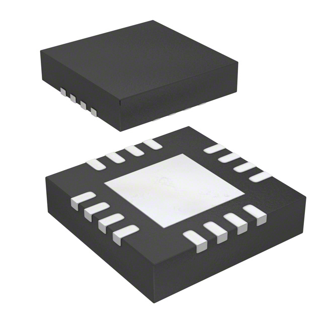


 工商网监
湘ICP备2023018690号
工商网监
湘ICP备2023018690号
