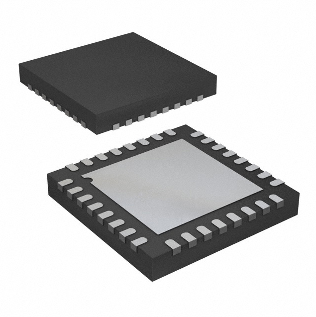
16-Bit, 10 MSPS, PulSAR Differential ADC AD7626
FEATURES
Throughput: 10 MSPS SNR: 91.5 dB 16-bit no missing codes INL: ±0.45 LSB DNL: ±0.35 LSB Power dissipation: 136mW 32-lead LFCSP (5 mm × 5 mm) SAR architecture No latency/no pipeline delay 16-bit resolution with no missing codes Zero error: ±1LSB Differential input range: ±4.096 V Serial LVDS interface Self-clocked mode Echoed-clock mode LVDS or CMOS option for conversion control (CNV signal) Reference options Internal: 4.096 V External (1.2 V) buffered to 4.096 V External: 4.096 V
FUNCTIONAL BLOCK DIAGRAM
REFIN REF VCM
1.2V BAND GAP IN+ IN– CAP DAC
÷2
CLOCK LOGIC
VIO
CNV+, CNV–
D+, D–
AD7626
Figure 1.
CLK+, CLK–
GENERAL DESCRIPTION
The AD7626 is a 16-bit, 10 MSPS, charge redistribution successive approximation register (SAR) based architecture analog-to-digital converter (ADC). SAR architecture allows unmatched performance both in noise (91.5 dB SNR) and in linearity (±0.45 LSB INL). The AD7626 contains a high speed, 16-bit sampling ADC, an internal conversion clock, and an internal buffered reference. On the CNV edge, it samples the voltage difference between the IN+ and IN− pins. The voltages on these pins swing in opposite phase between 0 V and REF. The 4.096 V reference voltage, REF, can be generated internally or applied externally. All converted results are available on a single LVDS self-clocked or echoed-clock serial interface, reducing external hardware connections. The AD7626 is housed in a 32-lead, 5 mm × 5 mm LFCSP with operation specified from −40°C to +85°C.
APPLICATIONS
Digital imaging systems Digital X-ray Digital MRI CCD and IR cameras High speed data acquisition High dynamic range telecommunications receivers Spectrum analysis Test equipment
Table 1. Fast PulSAR® ADC Selection
Input Type Differential (Ground Sense) Resolution (Bits) 16 1 MSPS to 4.3 V applied to the REF pin. 3 Transient currents of up to 100 mA do not cause SCR latch-up.
Stresses above those listed under Absolute Maximum Ratings may cause permanent damage to the device. This is a stress rating only; functional operation of the device at these or any other conditions above those indicated in the operational section of this specification is not implied. Exposure to absolute maximum rating conditions for extended periods may affect device reliability.
Rev. A | Page 7 of
�AD7626 PIN CONFIGURATION AND FUNCTION DESCRIPTIONS
32 31 30 29 28 27 26 25
REF GND REF REF CAP2 GND CAP2 CAP2
VDD1 VDD2 CAP1 REFIN EN0 EN1 VDD2 CNV–
1 2 3 4 5 6 7 8
PIN 1 INDICATOR
AD7626
TOP VIEW (Not to Scale)
24 23 22 21 20 19 18 17
GND IN+ IN– VCM VDD1 VDD1 VDD2 CLK+
CNV+ D– D+ VIO GND DCO– DCO+ CLK–
9 10 11 12 13 14 15 16
NOTES 1. CONNECT THE EXPOSED PAD TO THE GROUND PLANE OF THE PCB USING MULTIPLE VIAS.
Figure 4. Pin Configuration
Table 6. Pin Function Descriptions
Pin No. 1 2 3 4 Mnemonic VDD1 VDD2 CAP1 REFIN Type1 P P AO AI/O Description Analog 5 V Supply. Decouple the 5 V supply with a 100 nF capacitor. Analog 2.5 V Supply. Decouple this pin with a 100 nF capacitor. The 2.5 V supply source should supply this pin first, then be traced to the other VDD2 pins (Pin 7 and Pin 18). Connect this pin to a 10 nF capacitor. Prebuffer Reference Voltage. When using the internal reference, this pin outputs the band gap voltage and is nominally at 1.2 V. It can be overdriven with an external reference voltage such as the ADR280. In either internal or external reference mode, a 10 μF capacitor is required. If using an external 4.096 V reference (connected to REF), this pin is a no connect and does not require any capacitor. Enable. Operates from 2.5 V logic. The logic levels of these pins set the operation of the device as follows: EN1 = 0, EN0 = 0: power-down mode. EN1 = 0, EN0 = 1: external 1.2 V reference applied to the REFIN pin required. EN1 = 1, EN0 = 0: external 4.096 V reference applied to the REF pin required. EN1 = 1, EN0 = 1: internal reference and internal reference buffer in use. Digital 2.5 V Supply. Decouple this pin with a 100 nF capacitor. Convert Input. These pins act as the conversion control pin. On the rising edge of these pins, the analog inputs are sampled and a conversion cycle is initiated. CNV+ works as a CMOS input when CNV− is grounded; otherwise, CNV+ and CNV− are differential LVDS inputs. LVDS Data Outputs. The conversion data is output serially on these pins. Input/Output Interface Supply. Use a 2.5 V supply and decouple this pin with a 100 nF capacitor. Ground. Return path for the 100 nF capacitor connected to Pin 12. LVDS Buffered Clock Outputs. When DCO+ is grounded, the self-clocked interface mode is selected. In this mode, the 16-bit results on D are preceded by an initial 0 (which is output at the end of the previous conversion), followed by a 2-bit header (10) to allow synchronization of the data by the digital host with extra logic. The 1 in this header provides the reference to acquire the subsequent conversion result correctly. When DCO+ is not grounded, the echoed-clock interface mode is selected. In this mode, DCO± is a copy of CLK±. The data bits are output on the falling edge of DCO+ and can be captured in the digital host on the next rising edge of DCO+. LVDS Clock Inputs. This clock shifts out the conversion results on the falling edge of CLK+. Analog 2.5 V Supply. Decouple this pin with a 100 nF capacitor. Analog 5 V Supply. Isolate these pins from Pin 1 with a ferrite bead and decouple them with a 100 nF capacitor. Common-Mode Output. When using any reference scheme, this pin produces one-half the voltage present on the REF pin, which can be useful for driving the common mode of the input amplifiers. Differential Negative Analog Input. Referenced to and must be driven 180° out of phase with IN+.
Rev. A | Page 8 of 28
5, 6
EN0, EN1
DI
7 8, 9
VDD2 CNV−, CNV+
P DI
10, 11 12 13 14, 15
D−, D+ VIO GND DCO−, DCO+
DO P P DO
16, 17 18 19, 20 21 22
CLK−, CLK+ VDD2 VDD1 VCM IN−
DI P P AO AI
07648-002
�AD7626
Pin No. 23 24 25, 26, 28 27 29, 30, 32 Mnemonic IN+ GND CAP2 GND REF Type 1 AI P AO P AI/O Description Differential Positive Analog Input. Referenced to and must be driven 180° out of phase with IN−. Ground. Connect all three CAP2 pins together and decouple them with the shortest trace possible to a single 10 μF, low ESR, low ESL capacitor. The other side of the capacitor must be placed close to Pin 27 (GND). Ground. Return path for the 10 μF capacitor connected to Pin 25, Pin 26, and Pin 28. Buffered Reference Voltage. When using the internal reference or the 1.2 V external reference (REFIN input), the 4.096 V system reference is produced at this pin. When using an external reference, such as the ADR434 or the ADR444, the internal reference buffer must be disabled. In either case, connect all three REF pins together and decouple them with the shortest trace possible to a single 10 μF, low ESR, low ESL capacitor. The other side of the capacitor must be placed close to Pin 31 (GND). Ground. Return path for the 10 μF capacitor connected to Pin 29, Pin 30, and Pin 32. The exposed pad is located on the underside of the package. Connect the exposed pad to the ground plane of the PCB using multiple vias. See the Exposed Paddle section for more information.
31 EP
1
GND Exposed pad
P
AI = analog input; AI/O = bidirectional analog; AO = analog output; DI = digital input; DO = digital output; P = power.
Rev. A | Page 9 of
�AD7626 TYPICAL PERFORMANCE CHARACTERISTICS
VDD1 = 5 V; VDD2 = 2.5 V; VIO = 2.5 V; REF = 4.096 V; all plots at 10 MSPS unless otherwise noted. FFT plots for 2 MHz, 3 MHz, and 5 MHz input tones use band pass filter (±400 kHz pass bandwidth around fundamental frequency).
0 –20 –40
AMPLITUDE (dB)
INPUT FREQUENCY = 10.37kHz SNR = 91.85dB SINAD = 91.8dB THD = –112.1dB SFDR = 112.85dB 32k SAMPLES
AMPLITUDE (dB)
0 –20 –40 –60 –80 –100 –120 –140 –160
07648-108
INPUT FREQUENCY = 100kHz SNR = 91.323dB SINAD = 91.047dB THD = –102.543dB SFDR = 104.529dB
–60 –80 –100 –120 –140 –160 –180 0 10 30 50 FREQUENCY (kHz) 70 90
0
0.5
1.0
1.5
2.0
2.5
3.0
3.5
4.0
4.5
5.0
FREQUENCY (MHz)
Figure 5. 10 kHz, −0.5 dB Input Tone, Zoomed View
0 –20 –40
AMPLITUDE (dB)
INPUT FREQUENCY = 2.0026MHz –0.5dB INPUT AMPLITUDE SNR = 87.4dBFS SINAD = 84.8dBFS THD = –87.9dB SFDR = 88.1dB 64k SAMPLES
Figure 8.100 kHz, −0.5 dB Input Tone FFT, Full Frequency View
0 –20 –40
AMPLITUDE (dB)
INPUT FREQUENCY = 2.0026MHz –6dB INPUT AMPLITUDE SNR = 87.6dBFS SINAD = 87.6dBFS THD = –101.6dB SFDR = 101.9dB 64k SAMPLES
–60 –80 –100 –120 –140 –160
FIFTH HARMONIC
THIRD HARMONIC SECOND HARMONIC
–60 –80 –100 –120 –140 –160
FIFTH HARMONIC
THIRD HARMONIC
SECOND HARMONIC
07648-402
0
0.5
1.0
1.5
2.0
2.5
3.0
3.5
4.0
4.5
5.0
0
0.5
1.0
1.5
2.0
2.5
3.0
3.5
4.0
4.5
5.0
FREQUENCY (MHz)
FREQUENCY (MHz)
Figure 6. FFT, 2 MHz, −0.5 dB Input Tone, Wide View
Figure 9. FFT, 2 MHz, −6 dB Input Tone, Wide View
0 –20 –40
AMPLITUDE (dB)
INPUT FREQUENCY = 3.00125MHz –0.5dB INPUT AMPLITUDE SNR = 87.1dBFS SINAD = 81.2dBFS THD = –82.0dB SFDR = 82.1dB 64k SAMPLES THIRD HARMONIC SECOND HARMONIC FIFTH HARMONIC
0 –20 –40
AMPLITUDE (dB)
INPUT FREQUENCY = 3.00125MHz –6dB INPUT AMPLITUDE SNR = 88.48dBFS SINAD = 88.3dBFS THD = –97.2dB SFDR = 98.3dB 64k SAMPLES
–60 –80 –100 –120 –140 –160
–60 –80
THIRD HARMONIC
FOURTH HARMONIC
–100 –120 –140 –160
SECOND HARMONIC FOURTH HARMONIC
FIFTH HARMONIC
07648-404
0
0.5
1.0
1.5
2.0
2.5
3.0
3.5
4.0
4.5
5.0
0
0.5
1.0
1.5
2.0
2.5
3.0
3.5
4.0
4.5
5.0
FREQUENCY (MHz)
FREQUENCY (MHz)
Figure 7. FFT, 3 MHz, −0.5 dB Input Tone, Wide View
Figure 10. FFT, 3 MHz, −6 dB Input Tone, Wide View
Rev. A | Page 10 of
07648-411
–180
–180
07648-409
–180
–180
07648-118
–180
�AD7626
0 –20 –40
AMPLITUDE (dB)
INPUT FREQUENCY = 5.00656128MHz –0.5dB INPUT AMPLITUDE SNR = 86.7dBFS SINAD = 83.2dBFS THD = –85.3dB SFDR = 86.1dB 64k SAMPLES THIRD HARMONIC SECOND HARMONIC FOURTH HARMONIC FIFTH HARMONIC
0 –20 –40
AMPLITUDE (dB)
INPUT FREQUENCY = 5.00656128MHz –0.5dB INPUT AMPLITUDE SNR = 86.7dBFS SINAD = 83.2dBFS THD = –85.3dB SFDR = 86.1dB 64k SAMPLES
FUNDAMENTAL
–60 –80 –100 –120 –140 –160
–60 –80 –100 –120 –140 –160
THIRD HARMONIC FIFTH HARMONIC
07648-406
0
0.5
1.0
1.5
2.0
2.5
3.0
3.5
4.0
4.5
5.0
4.55
4.60
4.65
4.70
4.75
4.80
4.85
4.90
4.95
5.00
FREQUENCY (MHz)
FREQUENCY (MHz)
Figure 11. FFT, 5 MHz, −0.5 dB Input Tone, Wide View
Figure 14. FFT, 5 MHz, −0.5 dB Input Tone Zoomed View
0 –20 –40
AMPLITUDE (dB)
INPUT FREQUENCY = 5.00656128MHz –6dB INPUT AMPLITUDE SNR = 88.4dBFS SINAD = 88.0dBFS THD = –92.4dB SFDR = 92.8dB 64k SAMPLES
0 –20
FUNDAMENTAL INPUT FREQUENCY = 5.00656128MHz –6dB INPUT AMPLITUDE SNR = 88.4dBFS SINAD = 88.0dBFS THD = –92.4dB SFDR = 92.8dB 64k SAMPLES
FUNDAMENTAL
–40
AMPLITUDE (dB)
–60 –80 –100 –120 –140 –160
07648-413
–60 –80 –100 –120 –140 –160
07648-407 07648-401
SECOND HARMONIC FOURTH HARMONIC
THIRD HARMONIC
THIRD HARMONIC FIFTH HARMONIC
FIFTH HARMONIC
–180 0 0.5 1.0 1.5 2.0 2.5 3.0 3.5 4.0 4.5 5.0 FREQUENCY (MHz)
–180 4.50
4.55
4.60
4.65
4.70
4.75
4.80
4.85
4.90
4.95
5.00
FREQUENCY (MHz)
Figure 12. FFT, 5 MHz, −6 dB Input Tone, Wide View
–75 –80 –85 5MHz
SNR (dBFS)
Figure 15. FFT, 5 MHz, −0.5 dB Input Tone Zoomed View
94 92 90 –70 88 86 –90 84
THD (dB)
–50
9.7MHz
–60
–90
THD (dB)
SNR –80
–95 1MHz –100 –105 –110 2MHz –15 –12 –9 –6 –3 0
07648-211
3MHz
82 THD 80 10k 100k 1M
–100
–115 –18
–110 10M
INPUT AMPLITUDE (dBFS)
INPUT FREQUENCY (Hz)
Figure 13. THD vs. Input Amplitudes at Input Frequency Tones of 10 kHz to 9.7 MHz
Figure 16. THD and SNR vs. Input Frequency (−0.5 dB Input Tone)
Rev. A | Page 11 of
07648-412
–180
–180 4.50
�AD7626
92.0 91.8 91.6 91.4 EXTERNAL REFERENCE
SINAD (dB) SNR (dB)
92.0 91.8 91.6 91.4 91.2 91.0 90.8 90.6 90.4 90.2
07648-212 07648-215
91.2 91.0 90.8
EXTERNAL REFERENCE
INTERNAL REFERENCE 90.6 90.4 90.2 90.0 –40 INTERNAL REFERENCE
–20
0
20
40
60
80
90.0 –40
–20
0
20
40
60
80
TEMPERATURE (°C)
TEMPERATURE (°C)
Figure 17. SNR vs. Temperature (−0.5 dB, 20 kHz Input Tone)
Figure 20. SINAD vs. Temperature (−0.5 dB, 20 kHz Input Tone)
0.35
ZERO ERROR AND GAIN ERROR (LSB)
7 6 5 4 3 2 1 0 –1 –40 ZERO ERROR GAIN ERROR
0.30 0.25
INPUT URRENT (mA)
+INPUT CURRENT 0.20 0.15 0.10 0.05 –INPUT CURRENT 0 –0.05
07648-121
–4
–2
0
2
4
6
–20
0
20
40
60
80
INPUT COMMON-MODE VOLTAGE (V)
TEMPERATURE (°C)
Figure 18. Input Current (IN+, IN−) vs. Differential Input Voltage (10 MSPS)
Figure 21. Zero Error and Gain Error vs. Temperature
–103.0 –103.5
250,000
262,144 SAMPLES STD DEVIATION = 0.4829 201,320
200,000
–104.0 –104.5
THD (dB)
EXTERNAL REFERENCE
150,000
COUNT
–105.0 –105.5 –106.0 INTERNAL REFERENCE –106.5 –107.0 –40
100,000
50,000
30,651 30,073
07648-214
–20
0
20
40
60
80
FEC7
FEC8
FEC9
FECA CODE (HEX)
FECB
FECC
FECD
TEMPERATURE (°C)
Figure 19. THD vs. Temperature (−0.5 dB, 20 kHz Input Tone)
Figure 22. Histogram of 262,144 Conversions of a DC Input at the Code Center (Internal Reference)
Rev. A | Page 12 of 2
07648-022
0
0
54
46
0
07648-301
–0.10 –6
�AD7626
250,000
262,144 SAMPLES STD DEVIATION = 0.4814
0.30 0.25 0.20 0.15 0.10
200,000
201,614
DNL (LSB)
30,206 30,250 0 41 33 0
150,000
COUNT
0.05 0 –0.05 –0.10 –0.15
100,000
50,000
–0.20 –0.25
FEC8
FEC9
FECA
FECB
FECC
FECD
FECE
07648-024
0
16,384
32,768 CODE
49,152
65,536
CODE (HEX)
Figure 23. Histogram of 262,144 Conversions of a DC Input at the Code Center (External Reference)
140,000
128,084 129,601 262,144 SAMPLES STD DEVIATION = 0.5329
Figure 25. Differential Nonlinearity vs. Code (25ºC)
0.8 0.6 0.4 0.2 +85°C +25°C –40°C
120,000 100,000
COUNT
80,000
INL (LSB)
0 –0.2
60,000 40,000
–0.4 20,000
0 2130 2329 0
07648-023
–0.6 –0.8 0 16,384 32,768 CODE 49,152 65,536
FEC6
FEC7
FEC8
FEC9
FECA
FECB
CODE (HEX)
Figure 24. Histogram of 262,144 Conversions of a DC Input at the Code Transition
Figure 26. Integral Nonlinearity vs. Code vs. Temperature
Rev. A | Page 13 of
07648-115
0
07648-112
0
–0.30
�AD7626 TERMINOLOGY
Common-Mode Rejection Ratio (CMRR) CMRR is defined as the ratio of the power in the ADC output at full-scale frequency, f, to the power of a 100 mV p-p sine wave applied to the common-mode voltage of VIN+ and VIN− at frequency, fS. CMRR (dB) = 10 log(Pf/PfS) where: Pf is the power at frequency, f, in the ADC output. PfS is the power at frequency, fS, in the ADC output. Differential Nonlinearity (DNL) Error In an ideal ADC, code transitions are 1 LSB apart. Differential nonlinearity is the maximum deviation from this ideal value. It is often specified in terms of resolution for which no missing codes are guaranteed. Integral Nonlinearity (INL) Error Linearity error refers to the deviation of each individual code from a line drawn from negative full scale through positive full scale. The point used as negative full scale occurs ½ LSB before the first code transition. Positive full scale is defined as a level 1½ LSB beyond the last code transition. The deviation is measured from the middle of each code to the true straight line. Dynamic Range Dynamic range is the ratio of the rms value of the full scale to the rms noise measured for an input typically at −60 dB. The value for dynamic range is expressed in decibels. Effective Number of Bits (ENOB) ENOB is a measurement of the resolution with a sine wave input. It is related to SINAD and is expressed in bits by ENOB = [(SINADdB − 1.76)/6.02] Gain Error The first transition (from 100 … 000 to 100 …001) should occur at a level ½ LSB above nominal negative full scale (−4.0959375 V for the ±4.096 V range). The last transition (from 011 … 110 to 011 … 111) should occur for an analog voltage 1½ LSB below the nominal full scale (+4.0959375 V for the ±4.096 V range). The gain error is the deviation of the difference between the actual level of the last transition and the actual level of the first transition from the difference between the ideal levels. Gain Error Drift The ratio of the gain error change due to a temperature change of 1°C and the full-scale range (2N). It is expressed in parts per million. Least Significant Bit (LSB) The least significant bit, or LSB, is the smallest increment that can be represented by a converter. For a fully differential input ADC with N bits of resolution, the LSB expressed in volts is Power Supply Rejection Ratio (PSRR) Variations in power supply affect the full-scale transition but not the linearity of the converter. PSRR is the maximum change in the full-scale transition point due to a change in power supply voltage from the nominal value. Reference Voltage Temperature Coefficient The reference voltage temperature coefficient is derived from the typical shift of output voltage at 25°C on a sample of parts at the maximum and minimum reference output voltage (VREF) measured at TMIN, T(25°C), and TMAX. It is expressed in ppm/°C as
TCVREF ( ppm/°C ) = VREF ( Max ) – VREF ( Min ) VREF ( 25°C ) × ( TMAX – TMIN ) ×10 6
where: VREF (Max) = maximum VREF at TMIN, T(25°C), or TMAX. VREF (Min) = minimum VREF at TMIN, T(25°C), or TMAX. VREF (25°C) = VREF at 25°C. TMAX = +85°C. TMIN = −40°C.
Signal-to-Noise Ratio (SNR) SNR is the ratio of the rms value of the actual input signal to the rms sum of all other spectral components below the Nyquist frequency, excluding harmonics and dc. The value for SNR is expressed in decibels. Signal-to-(Noise + Distortion) Ratio (SINAD) SINAD is the ratio of the rms value of the actual input signal to the rms sum of all other spectral components below the Nyquist frequency, including harmonics but excluding dc. The value for SINAD is expressed in decibels. Spurious-Free Dynamic Range (SFDR) SFDR is the difference, in decibels, between the rms amplitude of the input signal and the peak spurious signal (including harmonics). Total Harmonic Distortion (THD) THD is the ratio of the rms sum of the first five harmonic components to the rms value of a full-scale input signal and is expressed in decibels. Zero Error Zero error is the difference between the ideal midscale input voltage (0 V) and the actual voltage producing the midscale output code. Zero Error Drift
The ratio of the zero error change due to a temperature change of 1°C and the full scale code range (2N). It is expressed in parts per million.
LSB (V) =
V INp-p 2N
Rev. A | Page 14 of
�AD7626 THEORY OF OPERATION
IN+ GND
SWITCHES CONTROL
MSB 32,768C 16,384C REF (4.096V) 4C 2C C C
LSB
SW+
CLK+, CLK–
COMP GND 32,768C 16,384C MSB 4C 2C C C LSB GND IN– SW–
CONTROL LOGIC
DCO+, DCO– D+, D– OUTPUT CODE
DATA TRANSFER
CNV+, CNV–
CONVERSION CONTROL
LVDS INTERFACE
07648-030
Figure 27. ADC Simplified Schematic
CIRCUIT INFORMATION
The AD7626 is a 10 MSPS, high precision, power efficient, 16-bit ADC that uses SAR-based architecture to provide a performance of 91.5 dB SNR, ±0.45 LSB INL, and ±0.35 LSB DNL. The AD7626 is capable of converting 10,000,000 samples per second (10 MSPS). The device typically consumes 136 mW of power. The AD7626 offers the added functionality of a high performance on-chip reference and on-chip reference buffer. The AD7626 is specified for use with 5 V and 2.5 V supplies (VDD1, VDD2). The interface from the digital host to the AD7626 uses 2.5 V logic only. The AD7626 uses an LVDS interface to transfer data conversions. The CNV+ and CNV− inputs to the part activate the conversion of the analog input. The CNV+ and CNV− pins can be applied using a CMOS or LVDS source. The AD7626 is housed in a space-saving, 32-lead, 5 mm × 5 mm LFCSP. When the conversion phase begins, SW+ and SW− are opened first. The two capacitor arrays are then disconnected from the inputs and connected to the GND input. Therefore, the differential voltage between the inputs (IN+ and IN−) captured at the end of the acquisition phase is applied to the comparator inputs, causing the comparator to become unbalanced. By switching each element of the capacitor array between GND and 4.096 V (the reference voltage), the comparator input varies by binary weighted voltage steps (VREF/2, VREF/4 … VREF/65,536). The control logic toggles these switches, MSB first, to bring the comparator back into a balanced condition. At the completion of this process, the control logic generates the ADC output code. The AD7626 digital interface uses low voltage differential signaling (LVDS) to enable high data transfer rates. The AD7626 conversion result is available for reading after tMSB (time from the conversion start until MSB is available) has elapsed. The user must apply a burst LVDS CLK± signal to the AD7626 to transfer data to the digital host. The CLK± signal outputs the ADC conversion result onto the data output D±. The bursting of the CLK± signal is illustrated in Figure 41 and Figure 42 and is characterized as follows:
• •
CONVERTER INFORMATION
The AD7626 is a 10 MSPS ADC that uses SAR-based architecture to incorporate a charge redistribution DAC. Figure 27 shows a simplified schematic of the ADC. The capacitive DAC consists of two identical arrays of 16 binary weighted capacitors that are connected to the two comparator inputs. During the acquisition phase, the terminals of the array tied to the input of the comparator are connected to GND via SW+ and SW−. All independent switches are connected to the analog inputs. In this way, the capacitor arrays are used as sampling capacitors and acquire the analog signal on the IN+ and IN− inputs. A conversion phase is initiated when the acquisition phase is complete and the CNV input goes high. Note that the AD7626 can receive a CMOS or LVDS format CNV signal.
The differential voltage on CLK± should be held steady state in the time between tCLKL and tMSB. The AD7626 has two data read modes. For more information about the echoed-clock and self-clocked interface modes, see the Digital Interface section.
Rev. A | Page 15 of
�AD7626
TRANSFER FUNCTIONS
The AD7626 uses a 4.096 V reference. The AD7626 converts the differential voltage of the antiphase analog inputs (IN+ and IN−) into a digital output. The analog inputs, IN+ and IN−, require a 2.048 V common-mode voltage (REF/2). The 16-bit conversion result is in MSB first, twos complement format. The ideal transfer functions for the AD7626 are shown in Figure 28 and Table 7.
ADC CODE (TWOS COMPLEMENT)
ANALOG INPUTS
The analog inputs, IN+ and IN−, applied to the AD7626 must be 180° out of phase with each other. Figure 29 shows an equivalent circuit of the input structure of the AD7626. The two diodes provide ESD protection for the analog inputs, IN+ and IN−. Care must be taken to ensure that the analog input signal does not exceed the reference voltage by more than 0.3 V. If the analog input signal exceeds this level, the diodes become forward-biased and start conducting current. These diodes can handle a forward-biased current of 130 mA maximum. However, if the supplies of the input buffer (for example, the supplies of the ADA4899-1 in Figure 33) are different from those of the reference, the analog input signal may eventually exceed the supply rails by more than 0.3 V. In such a case (for example, an input buffer with a short circuit), the current limitation can be used to protect the part.
VDD1 67Ω CNV 25pF
011 ... 111 011 ... 110 011 ... 101
100 ... 010 100 ... 001 100 ... 000 –FSR
IN+ OR IN–
–FSR + 1LSB
–FSR + 0.5LSB
07648-031
+FSR – 1LSB +FSR – 1.5LSB
ANALOG INPUT
Figure 29. Equivalent Analog Input Circuit
Figure 28. ADC Ideal Transfer Functions (FSR = Full-Scale Range)
Table 7. Output Codes and Ideal Input Voltages
Analog Input (IN+ − IN−) REF = 4.096 V +4.095875V +125 μV 0V −125 μV −4.095875 V − 4.096 V Digital Output Code Twos Complement (Hex) 0x7FFF 0x0001 0x0000 0xFFFF 0x8001 0x8000
The analog input structure allows the sampling of the true differential signal between IN+ and IN−. By using these differential inputs, signals common to both inputs are rejected. The AD7626 shows some degradation in THD with higher analog input frequencies.
75
CMRR (dB)
Description FSR − 1 LSB Midscale + 1 LSB Midscale Midscale − 1 LSB −FSR + 1 LSB −FSR
70
65
60
55
50
1
10
100
1k
10k
100k
1M
10M
INPUT COMMON-MODE FREQUENCY (Hz)
Figure 30. Analog Input CMRR vs. Frequency
Rev. A | Page 16 of
07648-009
45
07648-010
�AD7626
TYPICAL CONNECTION DIAGRAM
V+
ADR434 8 ADR444 CAPACITOR ON OUTPUT FOR STABILITY VDD1 (5V) VDD2 (2.5V)
CREF 10µF1, 2
10µF1
100nF 100nF
32 31 30 29 28 27 26 25
GND
CAP2
GND
REF
REF
REF
CAP2
CAP2
GND 24
10nF ADR280 8 10µF VIO
CONTROL FOR ENABLE PINS VDD2 (2.5V)
1 2 3 4
VDD1 IN+ 23 VDD2 CAP1 REFIN EN0 EN1 VDD1 19 VDD2 VDD2 18 DCO+ DCO– CNV+ CNV– CLK+ CLK– 100nF GND VIO
VDD2 (2.5V)
IN+ IN– VCM
VDD1 (5V)
PADDLE IN– 22 VCM 21
SEE THE DRIVING THE AD7625 SECTION7
10kΩ 3
10kΩ
5 6 7
AD7626
VDD1 20 100nF
FERRITE BEAD6
100nF
CONVERSION4 CONTROL CMOS (CNV+ ONLY) OR LVDS CNV+ AND CNV– USING 100Ω TERMINATION RESISTOR
8
9
10
11
D+
D–
12
13
14
15 5
16
17
100Ω VIO (2.5V) 100Ω
100Ω
100Ω
DIGITAL INTERFACE SIGNALS
DIGITAL HOST LVDS TRANSMIT AND RECEIVE
1 2 3
Figure 31. Typical Application Diagram
Rev. A | Page 17 of
07648-027
SEE THE LAYOUT, DECOUPLING, AND GROUNDING SECTION. CREF IS USUALLY A 10µF CERAMIC CAPACITOR WITH LOW ESR AND ESL. USE PULL-UP OR PULL-DOWN RESISTORS TO CONTROL EN0 AND EN1 DURING POWER-UP. EN0 AND EN1 INPUTS CAN BE FIXED IN HARDWARE OR CONTROLLED USING A DIGITAL HOST (EN0 = 0 AND EN1 = 0 PUTS THE ADC IN POWER-DOWN). 4 OPTION TO USE A CMOS (CNV+) OR LVDS (CNV±) INPUT TO CONTROL CONVERSIONS. 5 TO ENABLE SELF-CLOCKED MODE, TIE DCO+ TO GND. 6 CONNECT PIN 19 AND PIN 20 TO VDD1 SUPPLY; ISOLATE THE TRACE TO PIN 19 AND PIN 20 FROM THE TRACE TO PIN 1 USING A FERRITE BEAD SIMILAR TO WURTH 74279266. 7 SEE THE DRIVING THE AD7626 SECTION FOR DETAILS ON AMPLIFIER CONFIGURATIONS. 8 SEE THE VOLTAGE REFERENCE OPTIONS SECTION FOR DETAILS.
�AD7626
DRIVING THE AD7626
Differential Analog Input Source
Figure 33 shows an ADA4899-1 driving each differential input to the AD7626.
ANALOG INPUT (UNIPOLAR 0V TO 4.096V) ADA4899-1 U1
Single-Ended-to-Differential Driver
For applications using unipolar analog signals, a singleended-to-differential driver (as shown in Figure 32) allows for a differential input into the part. This configuration, when provided with an input signal of 0 V to 4.096 V, produces a differential ±4.096 V with midscale at 2.048 V. The one-pole filter using R = 20 Ω and C = 56 pF provides a corner frequency of 140 MHz. The VCM output of the AD7626 can be buffered and then used to provide the required 2.048 V common-mode voltage.
590Ω
20Ω 56pF IN+
590Ω
AD7626
IN– 20Ω VCM 56pF 100nF V+
U2 100nF
ADA4899-1
Single-Ended or Fully Differential High Frequency Driver
In applications that require higher input frequency tones, the ADA4932-1 can be used to drive the inputs to the AD7626. The ADA4932-1 is a differential driver, which also allows the user the option of single-ended-to-differential conversion. Figure 34 shows the typical circuit for a 50 Ω source impedance (ac-coupled in this example). The input to the ADA4932-1 is configured to be balanced to the source impedance (in this case 50 Ω). Further information on balancing the input impedance to the source impedance can be found on the ADA4932-1 datasheet. The circuit shown in Figure 34 operates with an overall gain of ~0.5 when the termination input termination is taken into account. Alternatively, the ADA4932-1 can be used with a fully differential source—it acts as an inverting differential driver.
REF1 CREF 10µF2 +VS 20Ω 0V TO VREF 56pF –VS +VS IN– 20Ω VREF TO 0V 56pF –VS
+VS VCM BUFFERED VCM PIN OUTPUT GIVES THE REQUIRED 2.048V COMMON-MODE SUPPLY FOR ANALOG INPUTS. 0.1µF –VS
50Ω
V–
AD8031, AD8032
Figure 32. Single-Ended-to-Differential Driver Circuit Using ADA4899-1
CREF 10µF2
REF1
REF IN+
REFIN
ADA4899-1
AD7626
GND
VCM 2.048V
ADA4899-1
AD8031, AD8032
1SEE THE VOLTAGE REFERENCE OPTIONS SECTION. CONNECTION TO EXTERNAL REFERENCE SIGNALS 2C REF IS USUALLY A 10µF CERAMIC CAPACITOR WITH LOW ESL AND ESR.
07648-025
IS DEPENDENT ON THE EN1 AND EN0 SETTINGS.
DECOUPLE REF AND REFIN PINS AS PER THE EN1 AND EN0 RECOMMENDATIONS
Figure 33. Driving the AD7626 from a Differential Analog Source Using ADA4899-1
Rev. A | Page 18 of 8
07648-033
�AD7626
499Ω SINGLE-ENDED ANALOG INPUT AC-COUPLED 50Ω SOURCE R35 499Ω 53.6Ω GND +7.25V VDRV+ 5 6 7 8 9 GND C22 0.1µF C24 0.1µF VCM GND 20Ω 1 11 10 4 20Ω 56pF GND C15 0.1µF 499Ω GND IN+ IN– 56pF VCM
AD8031
100nF GND
+VS 2 C 499Ω 3 12 50Ω 53.6Ω –VS 16 15 14 GND –2.5V 13 +IN –IN PD
VOCM FB–
ADA4932-1
–OUT +OUT FB+
AD7626
PAD PAD
Figure 34. High Frequency Input Drive Circuit Using the ADA4932-1; Single-Ended-to Differential Configuration
Rev. A | Page 19 of
07648-130
�AD7626
VOLTAGE REFERENCE OPTIONS
The AD7626 allows flexible options for creating and buffering the reference voltage. The AD7626 conversions refer to 4.096 V only. The various options creating this 4.096 V reference are controlled by the EN1 and EN0 pins (see Table 8).
Table 8. Voltage Reference Options
Option A EN1 1 EN0 1 Reference Mode Power-up Internal reference and internal reference buffer in use External 1.2 V reference applied to REFIN pin required External 4.096 V reference applied to REF pin required. Power-down mode
B C
0 1 0
1 0 0
DECOUPLE THE REF AND REFIN PINS EXTERNALLY. 10µF 10µF
A
IN+
REF
REFIN
AD7626
IN–
07648-131
EN1 = 1 AND EN0 = 1
POWER-UP—INTERNAL REFERENCE AND REFERENCE BUFFER IN USE. NO EXTERNAL REFERENCE CIRCUITRY REQUIRED.
Figure 35. Powered Up, Internal Reference and Internal Reference Buffer
CONNECT 1.2V EXTERNAL REFERENCE TO REFIN PIN. 1.2V REFIN INPUT IS BUFFERED INTERNALLY. IT CREATES A 4.096V REFERENCE FOR THE ADC. DECOUPLE THE REF AND REFIN PINS EXTERNALLY
1.2V 10µF 10µF 0.1µF
ADR280
VOUT V– V+
(2.4V ≤ V+ ≥ 5.5V) V+ 0.1µF
B
IN+
REF
REFIN
AD7626
IN–
07648-132
07648-133
EN1 = 0 AND EN0 = 1
EXTERNAL 1.2V REFERENCE CONNECTED TO REFIN PIN IS REQUIRED.
Figure 36. External 1.2 V Reference Using Internal Reference Buffer
V+ (6.1V ≤ VIN ≥ 18V) VIN 10µF 0.1µF
ADR434/ ADR444
VIN VOUT GND
4.096V 0.1µF
AD8031
10µF
CONNECT BUFFERED 4.096V SIGNAL TO REF PIN. DECOUPLE THE REF PIN EXTERNALLY. REFIN IS A NO CONNECT.
NO CONNECT
C
IN+
REF
REFIN
AD7626
IN–
EN1 = 1 AND EN0 = 0
EXTERNAL 4.096V REFERENCE CONNECTED TO REF PIN IS REQUIRED.
Figure 37. External 4.096 V Reference Applied to REF Pin
Rev. A | Page 20 of 2
�AD7626
Wake-Up Time from EN1= 0, EN0 = 0
The AD7626 powers down when EN1 and EN0 are both set to 0. Selecting the correct reference choice from power-down, the user sets EN1 and EN0 to the required value shown in Table 8. The user may immediately apply CNV pulses to receive data conversion results. Typical wake-up times for the selected reference settings are shown in Table 9. Each time represents the duration from the EN1, EN0 logic transition to when the output of the ADC is settled to 0.5 LSB accuracy.
Table 9. Wake-Up Time from EN1=0, EN0 = 0
Wake-Up Time (0.5 LSB Accuracy) 9.5 sec
20 VIO INTERNAL REFERENCE VDD2 EXTERNAL REFERENCE
Power-Up
When powering up the AD7626 device, first apply the 2.5 V VDD2 supply and VIO voltage to the device. After the VIO and 2.5 V VDD2 have been established, apply the 5 V VDD1 supply. If using an external reference with the AD7626, ensure that the EN0 and EN1 pins are connected to the correct logic values associated with the reference option of choice and then apply the external reference voltage. Finally, apply the analog inputs to the ADC.
25 VDD2 INTERNAL REFERENCE
A
B C
Reference Mode Power-up Internal reference and internal reference buffer in use External 1.2 V reference applied to REFIN pin External 4.096 V reference applied to REF pin
CURRENT (mA)
EN1 1
EN0 1
15
VIO EXTERNAL REFERENCE 10 VDD1 INTERNAL REFERENCE
0 1
1 0
25 ms 65 μs
5 VDD1 EXTERNAL REFERENCE 0 2 4 6 8 10
07648-235
POWER SUPPLY
The AD7626 uses both 5 V (VDD1) and 2.5 V (VDD2) power supplies, as well as a digital input/output interface supply (VIO). VIO allows a direct interface with 2.5 V logic only. VIO and VDD2 can be taken from the same 2.5 V source; however, it is best practice to isolate the VIO and VDD2 pins using separate traces as well as to decouple each pin separately. The 5 V and 2.5 V supplies required for the AD7626 can be generated using Analog Devices, Inc., LDOs such as the ADP3330-2.5, ADP3330-5, ADP3334, and ADP1708.
90 VDD2 85 80 VDD1 75
PSRR (dB)
0 THROUGHPUT (MSPS)
Figure 39. Current Consumption vs. Sampling Rate
160 140 INTERNAL REFERENCE 120 EXTERNAL REFERENCE
POWER (mW)
100 80 60 40 20 0 0 1 2 3 4 5 6 7 8 9 10 THROUGHPUT (MSPS)
70 65 60 55 INTERNAL REFERENCE USED 1 10 100 SUPPLY FREQUENCY (Hz) 1k 10k
07648-011
Figure 40. Power Dissipation vs. Sampling Rate
50
Figure 38. PSRR vs. Supply Frequency (350 mV pp Ripple on VDD2, 600 mV Ripple on VDD1)
Rev. A | Page 21 of 2
07648-236
�AD7626
DIGITAL INTERFACE
Conversion Control
All analog-to-digital conversions are controlled by the CNV± signal. This signal can be applied in the form of a CNV+/CNV− LVDS signal, or it can be applied in the form of a 2.5 V CMOS logic signal to the CNV+ pin. The conversion is initiated by the rising edge of the CNV± signal. After the AD7626 is powered up, the first conversion result generated is invalid. Subsequent conversion results are valid provided that the time between conversions does not exceed the maximum specification for tCYC. The two methods for acquiring the digital data output of the AD7626 via the LVDS interface are described in the following sections. The clock DCO± is a buffered copy of CLK± and is synchronous to the data, D±, which is updated on the falling edge of DCO + (tD). By maintaining good propagation delay matching between D± and DCO± through the board and the digital host, DCO can be used to latch D± with good timing margin for the shift register. Conversions are initiated by a rising edge CNV± pulse. The CNV± pulse must be returned low (≤ tCNVH maximum) for valid operation. After a conversion begins, it continues until completion. Additional CNV± pulses are ignored during the conversion phase. After the time, tMSB, elapses, the host should begin to burst the CLK±. Note that, tMSB, is the maximum time for the MSB of the new conversion result and should be used as the gating device for CLK±. The echoed clock, DCO±, and the data, D, are driven in phase with D± being updated on the falling edge of DCO+; the host should use the rising edge of DCO+ to capture D±. The only requirement is that the 16 CLK± pulses finish before the time (tCLKL) elapses of the next conversion phase or the data is lost. From the tCLKL to tMSB, D± and DCO± are driven to 0. Set CLK± to idle low between CLK± bursts.
Echoed-Clock Interface Mode
The digital operation of the AD7626 in echoed-clock interface mode is shown in Figure 41. This interface mode, requiring only a shift register on the digital host, can be used with many digital hosts (such as FPGA, shift register, and microprocessor). It requires three LVDS pairs (D±, CLK±, and DCO±) between each AD7626 and the digital host.
SAMPLE N
SAMPLE N + 1
tCYC tCNVH
CNV– CNV+
ACQUISITION
ACQUISITION
ACQUISITION
tCLK
CLK– CLK+ 15 16 1 2
tCLKL
15 16 1 2 3
tDCO
DCO– DCO+ 15 16 1 2 15 16
1
2
3
tCLKD
D+ D–
D1 N–1
tMSB
D0 N–1
tD
0
D15 N D14 N D1 N D0 N
0
D15 N+1
D14 N+1
D13 N+1
Figure 41. Echoed-Clock Interface Mode Timing Diagram
Rev. A | Page 22 of 2
07648-103
�AD7626
Self-Clocked Mode
The digital operation of the AD7626 in self-clocked interface mode is shown in Figure 42. This interface mode reduces the number of traces between the ADC and the digital host to two LVDS pairs (CLK± and D±) or to a single pair if sharing a common CLK±. Multiple AD7626 devices can share a common CLK± signal. This can be useful in reducing the number of LVDS connections to the digital host. When the self-clocked interface mode is used, each ADC data-word is preceded by a 010 sequence. The first zero is automatically on D± once tMSB has elapsed. The 2-bit header is then clocked out by the first two CLK± falling edges. This header is used to synchronize D± of each conversion in the digital host because, in this mode, there is no data clock output synchronous to the data (D±) to allow the digital host to acquire the data output. Synchronization of the D± data to the digital host’s acquisition clock is accomplished by using one state machine per AD7626 device. For example, using a state machine that runs at the same speed as CLK± incorporates three phases of this clock frequency (120º apart). Each phase acquires the data D± as output by the ADC. The AD7626 data captured on each phase of the state machine clock is then compared. The location of the 1 in the header in each set of data acquired allows the user to choose the state machine clock phase that occurs during the data valid window of D±. The self-clocked mode data capture method allows the digital host to adapt its result capture timing to accommodate variations in propagation delay through any AD7626.For example, where data is captured from multiple AD7626s sharing a common input clock. Conversions are initiated by a CNV± pulse. The CNV± pulse must be returned low (tCNVH maximum) for valid operation. After a conversion begins, it continues until completion. Additional CNV± pulses are ignored during the conversion phase. After the time, tMSB, elapses, the host begins to burst the CLK± signal to the AD7626. All 18 CLK± pulses are to be applied in the time window framed by tMSB and the subsequent tCLKL. The required 18 CLK± pulses must finish before tCLKL (referenced to the next conversion phase) elapses. Otherwise, the data is lost because it is overwritten by the next conversion result. Set CLK± to idle high between bursts of 18 CLK± pulses. The header bit and conversion data of the next ADC result are output on subsequent falling edges of CLK± during the next burst of the CLK± signal.
SAMPLE N + 1
SAMPLE N
tCYC tCNVH
CNV– CNV+
ACQUISITION
ACQUISITION
ACQUISITION
tCLK
CLK– CLK+ 17 18 1 2 3 4
tCLKL
17 18 1 2 3
tCLKD
D+ D– D1 N–1
tMSB
D0 N–1 0 1 0 D15 N D14 N D1 N D0 N 0 1 0 D15 N+1
07648-104
Figure 42. Self-Clocked Interface Mode Timing Diagram
Rev. A | Page 23 of 2
�AD7626 APPLICATIONS INFORMATION
LAYOUT, DECOUPLING, AND GROUNDING
When laying out the printed circuit board (PCB) for the AD7626, follow the practices described in this section to obtain the maximum performance from the converter.
VIO Supply Decoupling
Decouple the VIO supply applied to Pin 12 to ground at Pin 13.
Layout and Decoupling of Pin 25 to Pin 32
Connect the outputs of Pin 25, Pin 26, and Pin 28 together and decouple them to Pin 27 using a 10 μF capacitor with low ESR and low ESL. Reduce the inductance of the path connecting Pin 25, Pin 26, and Pin 28 by widening the PCB traces connecting these pins. Take a similar approach in the connections used for the reference pins of the AD7626. Connect Pin 29, Pin 30, and Pin 32 together using widened PCB traces to reduce inductance. In internal or external reference mode, a 4.096 V reference voltage is output on Pin 29, Pin 30, and Pin 32. Decouple these pins to Pin 31 using a 10 μF capacitor with low ESR and low ESL. Figure 43 shows an example of the recommended layout for the underside of the AD7626 device. Note the extended signal trace connections and the outline of the capacitors decoupling the signals applied to the REF pins (Pin 29, Pin 30, and Pin 32) and to the CAP2 pins (Pin 25, Pin 26, and Pin 28).
Exposed Paddle
The AD7626 has an exposed paddle on the underside of the package.
• • • •
Solder the paddle directly to the PCB. Connect the paddle to the ground plane of the board using multiple vias, as shown in Figure 43. Decouple all supply pins except for Pin 12 (VIO) directly to the paddle, minimizing the current return path. Pin 13 and Pin 24 can be connected directly to the paddle. Use vias to ground at the point where these pins connect to the paddle.
VDD1 Supply Routing and Decoupling
The VDD1 supply is connected to Pin 1, Pin 19, and Pin 20. Decouple the supply using a 100 nF capacitor at Pin 1. The user can connect this supply trace to Pin 19 and Pin 20. Use a series ferrite bead to connect the VDD1 supply from Pin 1 to Pin 19 and Pin 20. The ferrite bead isolates any high frequency noise or ringing on the VDD1 supply. Decouple the VDD1 supply to Pin 19 and Pin 20 using a 100 nF capacitor decoupled to ground at the exposed paddle.
24 23 22 21 20 19 18 17 25 4.096V EXTERNAL REFERENCE (ADR434 OR ADR444) 26 27 28 29 30 31 32 1 2 3 4 5 6 7 8
07648-013
16 PADDLE 15 14 13 12 11 10 9
Figure 43. PCB Layout and Decoupling Recommendations for Pin 24 to Pin 32
Rev. A | Page 24 of 2
�AD7626 OUTLINE DIMENSIONS
5.00 BSC SQ 0.60 MAX 0.60 MAX
25 24 32 1
PIN 1 INDICATOR
PIN 1 INDICATOR TOP VIEW 4.75 BSC SQ
0.50 BSC
EXPOSED PAD (BOTTOM VIEW)
17 16 8
3.25 3.10 SQ 2.95
0.50 0.40 0.30
9
0.25 MIN 3.50 REF
12° MAX
0.80 MAX 0.65 TYP 0.05 MAX 0.02 NOM
1.00 0.85 0.80
COMPLIANT TO JEDEC STANDARDS MO-220-VHHD-2
Figure 44. 32-Lead Lead Frame Chip Scale Package [LFCSP_VQ] 5 mm × 5 mm Body, Very Thin Quad (CP-32-2) Dimensions shown in millimeters
ORDERING GUIDE
Model 1 AD7626BCPZ AD7626BCPZ-RL7 EVAL-AD7626EDZ 2 EVAL-CED1Z 3
1 2
Temperature Range −40°C to +85°C −40°C to +85°C
Package Description 32-Lead Lead Frame Chip Scale Package [LFCSP_VQ] 32-Lead Lead Frame Chip Scale Package [LFCSP_VQ] Evaluation Board Converter Evaluation and Development Board
011708-A
SEATING PLANE
0.30 0.23 0.18
0.20 REF
COPLANARITY 0.08
FOR PROPER CONNECTION OF THE EXPOSED PAD, REFER TO THE PIN CONFIGURATION AND FUNCTION DESCRIPTIONS SECTION OF THIS DATA SHEET.
Package Option CP-32-2 CP-32-2
Z = RoHS Compliant Part. This board can be used as a standalone evaluation board or in conjunction with the EVAL-CEDIZ for evaluation/demonstration purposes. 3 This board allows the PC to control and communicate with all Analog Devices evaluation boards with model numbers ending with the ED designator.
Rev. A | Page 25 of 2
�AD7626 NOTES
Rev. A | Page 26 of 2
�AD7626 NOTES
Rev. A | Page 27 of 2
�AD7626 NOTES
©2009–2010 Analog Devices, Inc. All rights reserved. Trademarks and registered trademarks are the property of their respective owners. D07648-0-1/10(A)
Rev. A | Page 28 of 28
�


 工商网监
湘ICP备2023018690号
工商网监
湘ICP备2023018690号

