2.5 V/3.3 V, 8-Bit, 2-Port
Level Translating, Bus Switch
ADG3245
FEATURES
225 ps Propagation Delay through the Switch
4.5 ⍀ Switch Connection between Ports
Data Rate 1.244 Gbps
2.5 V/3.3 V Supply Operation
Selectable Level Shifting/Translation
Level Translation
3.3 V to 2.5 V
3.3 V to 1.8 V
2.5 V to 1.8 V
Small Signal Bandwidth 610 MHz
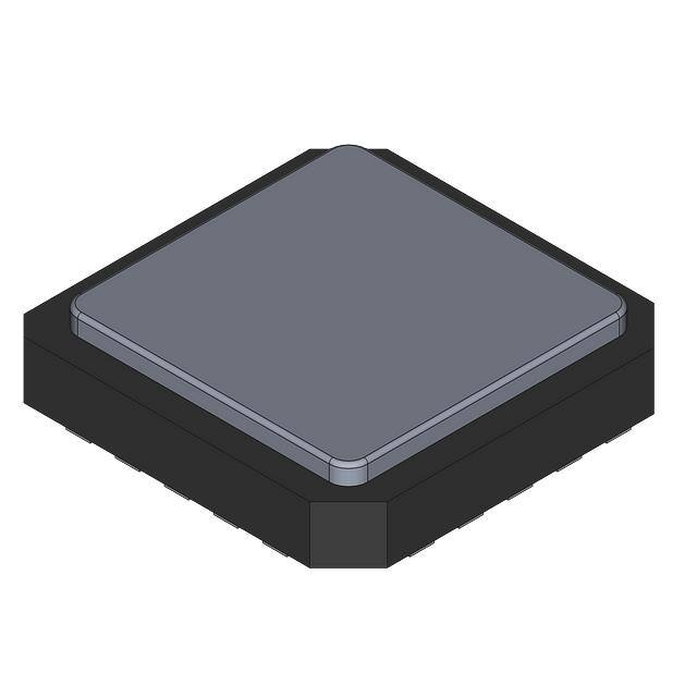
20-Lead TSSOP and LFCSP Packages
FUNCTIONAL BLOCK DIAGRAM
APPLICATIONS
3.3 V to 1.8 V Voltage Translation
3.3 V to 2.5 V Voltage Translation
2.5 V to 1.8 V Voltage Translation
Bus Switching
Bus Isolation
Hot Swap
Hot Plug
Analog Switch Applications
A0
B0
A7
B7
BE
GENERAL DESCRIPTION
PRODUCT HIGHLIGHTS
The ADG3245 is a 2.5 V or 3.3 V, 8-bit, 2-port digital switch.
It is designed on Analog Devices’ low voltage CMOS process,
which provides low power dissipation yet gives high switching
speed and very low on resistance, allowing inputs to be connected
to outputs without additional propagation delay or generating
additional ground bounce noise.
1.
2.
3.
4.
5.
3.3 V or 2.5 V supply operation
Extremely low propagation delay through switch
4.5 W switches connect inputs to outputs
Level/voltage translation
20-lead TSSOP and LFCSP (4 mm ¥ 4 mm) packages
The switches are enabled by means of the bus enable (BE) input
signal. These digital switches allow bidirectional signals to be
switched when ON. In the OFF condition, signal levels up to
the supplies are blocked.
This device is ideal for applications requiring level translation.
When operated from a 3.3 V supply, level translation from 3.3 V
inputs to 2.5 V outputs is allowed. Similarly, if the device is
operated from a 2.5 V supply and 2.5 V inputs are applied, the
device will translate the outputs to 1.8 V. In addition to this, a
level translating select pin (SEL) is included. When SEL is low,
VCC is reduced internally, allowing for level translation between
3.3 V inputs and 1.8 V outputs. This makes the device suited to
applications requiring level translation between different supplies,
such as converter to DSP/microcontroller interfacing.
REV. 0
Information furnished by Analog Devices is believed to be accurate and
reliable. However, no responsibility is assumed by Analog Devices for its
use, nor for any infringements of patents or other rights of third parties that
may result from its use. No license is granted by implication or otherwise
under any patent or patent rights of Analog Devices. Trademarks and
registered trademarks are the property of their respective companies.
One Technology Way, P.O. Box 9106, Norwood, MA 02062-9106, U.S.A.
Tel: 781/329-4700
www.analog.com
Fax: 781/326-8703
© 2003 Analog Devices, Inc. All rights reserved.
�ADG3245–SPECIFICATIONS1
Parameter
Symbol
DC ELECTRICAL CHARACTERISTICS
Input High Voltage
VINH
VINH
Input Low Voltage
VINL
VINL
Input Leakage Current
II
OFF State Leakage Current
IOZ
ON State Leakage Current
Maximum Pass Voltage
VP
CAPACITANCE3
A Port Off Capacitance
B Port Off Capacitance
A, B Port On Capacitance
Control Input Capacitance
SWITCHING CHARACTERISTICS3
Propagation Delay A to B or B to A, tPD4
Propagation Delay Matching5
Bus Enable Time BE to A or B6
Bus Disable Time BE to A or B6
Bus Enable Time BE to A or B6
Bus Disable Time BE to A or B6
Bus Enable Time BE to A or B6
Bus Disable Time BE to A or B6
Maximum Data Rate
Channel Jitter
Operating Frequency—Bus Enable
DIGITAL SWITCH
On Resistance
On Resistance Matching
POWER REQUIREMENTS
VCC
Quiescent Power Supply Current
Increase in ICC per Input7
(VCC = 2.3 V to 3.6 V, GND = 0 V, all specifications TMIN to TMAX, unless
otherwise noted.)
Conditions
Min
VCC = 2.7 V to 3.6 V
VCC = 2.3 V to 2.7 V
VCC = 2.7 V to 3.6 V
VCC = 2.3 V to 2.7 V
2.0
1.7
0 £ A, B £ VCC
0 £ A, B £ VCC
VA/VB = VCC = SEL = 3.3 V, IO = –5 mA
VA/VB = VCC = SEL = 2.5 V, IO= –5 mA
VA/VB = VCC = 3.3 V, SEL = 0 V, IO= –5 mA
CA OFF
CB OFF
CA, CB ON
CIN
f = 1 MHz
f = 1 MHz
f = 1 MHz
f = 1 MHz
tPHL, tPLH
CL = 50 pF, VCC = SEL = 3 V
tPZH, tPZL
tPHZ, tPLZ
tPZH, tPZL
tPHZ, tPLZ
tPZH, tPZL
tPHZ, tPLZ
VCC = 3.0 V to 3.6 V; SEL = VCC
VCC = 3.0 V to 3.6 V; SEL = VCC
VCC = 3.0 V to 3.6 V; SEL = 0 V
VCC = 3.0 V to 3.6 V; SEL = 0 V
VCC = 2.3 V to 2.7 V; SEL = VCC
VCC = 2.3 V to 2.7 V; SEL = VCC
VCC = SEL = 3.3 V; VA/VB = 2 V
VCC = SEL = 3.3 V; VA/VB = 2 V
2.0
1.5
1.5
B Version
Typ2
Max
± 0.01
± 0.01
± 0.01
2.5
1.8
1.8
5
5
10
6
1
1
0.5
0.5
0.5
0.5
3.2
3.2
2.2
1.7
2.2
1.75
1.244
50
fBE
RON
⌬RON
VCC = 3 V, SEL = VCC, VA = 0 V, IBA = 8 mA
VCC = 3 V, SEL = VCC, VA = 1.7 V, IBA = 8 mA
VCC = 2.3 V, SEL = VCC, VA = 0 V, IBA = 8 mA
VCC = 2.3 V, SEL = VCC, VA = 1 V, IBA = 8 mA
VCC = 3 V, SEL = 0 V VA = 0 V, IBA = 8 mA
VCC = 3 V, SEL = 0 V, VA = 1 V, IBA = 8 mA
VCC = 3 V, SEL = VCC, VA = 0 V, IBA = 8 mA
VCC = 3 V, SEL = VCC, VA = 1 V, IBA = 8 mA
4.5
15
5
11
5
14
0.45
0.65
⌬ICC
Digital Inputs = 0 V or VCC; SEL = VCC
Digital Inputs = 0 V or VCC ; SEL = 0 V
VCC = 3.6 V, BE = 3.0 V; SEL = VCC
0.001
0.65
V
V
V
V
mA
mA
mA
V
V
V
pF
pF
pF
pF
0.225
22.5
4.8
4.8
3.3
2.9
3
2.6
10
2.3
ICC
0.8
0.7
±1
±1
±1
2.9
2.1
2.1
Unit
ns
ps
ns
ns
ns
ns
ns
ns
Gbps
ps p-p
MHz
8
28
9
18
8
W
W
W
W
W
W
W
W
3.6
1
1.2
130
V
mA
mA
mA
NOTES
1
Temperature range is as follows: B Version: –40∞C to +85∞C.
2
Typical values are at 25∞C, unless otherwise stated.
3
Guaranteed by design, not subject to production test.
4
The digital switch contributes no propagation delay other than the RC delay of the typical R ON of the switch and the load capacitance when driven by an ideal voltage
source. Since the time constant is much smaller than the rise/fall times of typical driving signals, it adds very little propagation delay to the system. Propagation delay
of the digital switch when used in a system is determined by the driving circuit on the driving side of the switch and its interaction with the load on the driven side.
5
Propagation delay matching between channels is calculated from the on resistance matching and load capacitance of 50 pF.
6
See Timing Measurement Information section.
7
This current applies to the control pin BE only. The A and B ports contribute no significant ac or dc currents as they transition.
Specifications subject to change without notice.
–2–
REV. 0
�ADG3245
LFCSP Package
JA Thermal Impedance . . . . . . . . . . . . . . . . . . . . . .30.4°C/W
TSSOP Package
JA Thermal Impedance . . . . . . . . . . . . . . . . . . . . . . 143°C/W
Lead Temperature, Soldering (10 seconds) . . . . . . . . . . 300°C
IR Reflow, Peak Temperature (


 工商网监
湘ICP备2023018690号
工商网监
湘ICP备2023018690号
