ANALOGDEVICESFAX-ON-DEMAND
HOTLINE
- Page 2
"
-.
W
ANALOG
DEVICES
High-Speed
Voltage
FoIIowerIB uffe r
BUF-O3
I
in an open-loop circuit employing source followers and
FEATURES
.
very
.
High Slew Rate.
... .. . . .. .. ... .. ..,
220V/~1
Min
WideBandwidth
63MHz
. LoadDriveCurrent. . .. .. . . . . . . .. .. .. .. ... 70mA Peak
EasilyDrivesLarge CapacltlvttLoadsWithoutOscillation
. High Input Resistance. . . . . . .
.. .
5 X 10¹¹f!
.
..
Low Output Resistance
2f!
very Low Bla. Cum"t (Warmed-Up)
,. 400pA Max
LowOffaelVottage
6mVMax
. Unity Gain
,
0.997V/V
. EIceUenl Gain Linearity. . . . . . . . . , . . . . . . . . . . . .. 0.015'10
. Available In Die Form
.
OBS
emitterfollowers. the BUF-{)3utilizes a quasi-quad FETinput
structure to optimize both speed and D.C. input characteristics. On-chipzener-zap trimming is used to achieve low
offset voltage while careful biasing throughout results in
excell_entgain linearity over the full Input voltage range.
Applications for which the BUF-{)3is well-suited include
high-speed line drivers. isolation amplifiers for driving
reactive loads. and high-speed sample-hold circuits.
PIN CONNECTIONS
N.C.
.
ORDERINGINFORMATIONt
.
t
Ta = ZS.C
YOI MAX
(mY)
6
6
15
15
PACKAGE
TO-"
8-PlN
BUFO3AJBUF03EJ
BUF03BJ'
BUF03FJ
NUu.
OPERATING
TEMPERATURE
RANGE
Bum-In
Is availabltt
on commercia!
and
industria!
plasdc DIP. and T().can packages.
GENERAL DESCRIPTION
7 V.
OLE
0,
-
MIL
COM
MIL
COM
H.C.l.
IHPUTa
temperature
range
parts
TO-99 (J-Sufllx)
6 OIlTPUT
>HULl
.
V-(CASE)
For daYlces prOcess.d In Iolalcompliance to !.AIL-Sro-S83. add 18&3IfI8r part
number. Consult laclDryfor 883 data sh&8l.
.
c.rDIP,
"
TE
OPTIONAL OFFSET NULLING CIRCUIT
in
OUTPUT
The BUF-o3is the first very high-speedmonolithic voltage
follower. Featuring performance previously unobtainable Ina
monolithic unit. it offers a combination of both exceptional
speed and excellent input/output specifications. Implemented
SIMPLIFIED SCHEMATIC
y+
OUil'UT
INPlJT
0-..
v-
:"1-
--
�- Page
ANALOGDEVICESfA~-ON-DEMANDHOTLINE
3
.'
BUF-O3
ABSOLUTE MAXIMUM RATINGS
Supply Voltage
.
Internal PowerDissipation (Pd)
In Still Air Without Heat Sink (Note 1)
Input Voltage
Continuous
(Note
DiceJunction Temperature(Tj)
Thermal Resistance OJA(Note 1)
Thermal Resistance8JC(Note 1)
:t16V
""""""""""""""""'"
""""'"
l.00W
2)
,..
Output Current (Note 3)
NOTES:
1. Basedon
:t18V
MIL-STD-38510 published thermal resistance specification for 8
lallo can-case oulline C.
70mA
100mA
Peak Output Current (Note 3)
Short Circuit Protection
(Note 3)
-65°C to +175°C
150°CIW
18°CIW
Indefinite
2. When Vcc.-.:t 18V. the maximum input 'ollage
(Note 4)
Maximu.p_JunctionTemperature(Tj)
,
175°C
Storage Temperature Range. . . . . . . . . . .. -65°C to + 175°C
Operating Temperature Range (Note 5)
'
-55°C to + 125°C
Lead Temperature (Soldering, 60 sec)
300.C
is equal to tho supply 'oltage.
3. The maximum Pa or Tj are not to be exce.;ded.
4. At SOmA.
5. When operating
at TA > +25'C.
heat sinking is required
=
to insure TiMAX
+ 175'C specification is notexceedeo
using theequetton
Tjw.x- TA+ (Pa x
6JCMAX + 6SAi where 8M
sink to ambient thermal resistance.
PMI
=
recommenos using either the Thermalloy 2227 or 1101or equivalent when
operating up to TA=+ 12S'C.
ELECTRICAL CHARACTERISTICS at Vs"" :t15V. Rs'" DO,T" '" Tj = 25°C, unless otherwise noted. (Note 1)
OBS
PARAMETER
SYMBOL
BUF.O3A/E
MIH TYP MAX
CONDITIONS
BUF.O3B/F
IIIN
TVP MAX
UNITS
AC SPECIFICATIONS
Slew Rate
SR
Rl ~ 2kO. Cl = 50pF.
fJ 75'C
fA
POWilTBandwidtl'l
PBW
ts
To 0..1%,:t 10V step
CLOAO
td
Step Inpul
Rise Time
t,
~V
Wide Band InpUI Noise Voltage
Vn
DC to 50MHz
Inpul Noi..
en
I = 10kHz
Input Offset Voltage
Vas
RS~ 20kCl (Note 21
Inpul Bias Current
18
Propagation
Delay
Voltage Density
A'N
Voltage Gain (V'N= :t1DV)
Ava
-
350
-
50
0.9960
0.9945
0.9925
At ~ 10kO
Rl ~ 2kl)
RlP
+15V
3kn
QZ
2N:IIIO6
LOGIC
IN
HOLO;'
-,.W
RI
121
很抱歉,暂时无法提供与“BUF03EJ”相匹配的价格&库存,您可以联系我们找货
免费人工找货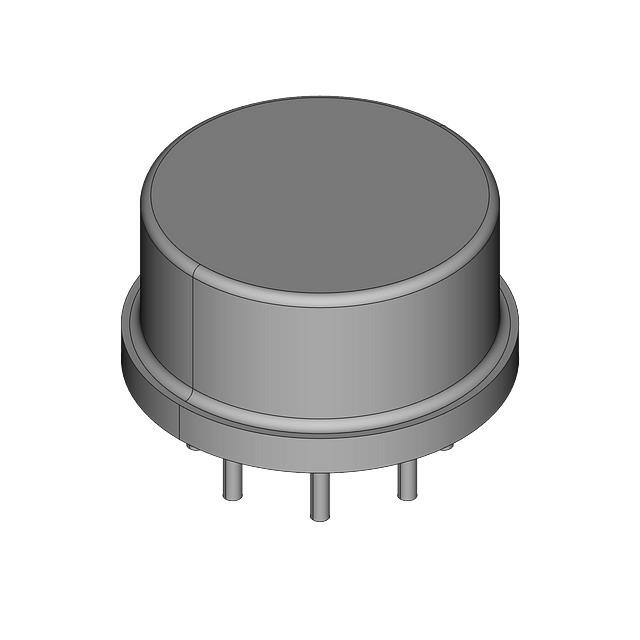


 工商网监
湘ICP备2023018690号
工商网监
湘ICP备2023018690号
