A4960
Sensorless BLDC Controller
Features and Benefits
Description
• 3-phase BLDC sensorless start-up and commutation
• Gate drive for N-channel MOSFETs
• Integrated PWM current limit
• 7 to 50 V supply voltage operating range
• Compatible with 3.3 V and 5 V logic
• Cross-conduction protection with adjustable dead time
• Charge pump for low supply voltage operation
• Extensive diagnostics output
• Low current sleep mode
The A4960 is a three-phase, sensorless, brushless DC (BLDC)
motor controller for use with external N-channel power
MOSFETs.
Applications:
An external bootstrap capacitor is used to provide the above
battery supply voltage required for N-channel MOSFETs.
An automatic internal bootstrap charge management scheme
ensures that the bootstrap capacitor is always sufficiently
charged for safe operation of the power MOSFETs. The power
MOSFETs are protected from shoot-through by integrated
crossover control and adjustable dead time.
The motor is driven using block commutation (trapezoidal
drive) where phase commutation is determined, without the
need for independent position sensors, by monitoring the motor
back-EMF. A programmable motor start-up scheme allows
the A4960 to be adjusted for a wide range of motor and load
combinations.
• Pumps
• Fans
• Blowers
Package: 32-pin LQFP with exposed
thermal pad (suffix JP)
Integrated diagnostics provide indication of undervoltage,
overtemperature, and power bridge faults and can be configured
to protect the power MOSFETs under most short circuit
conditions. Detailed diagnostics are available as a serial data
word.
The A4960 is supplied in a 32-pin LQFP with exposed pad
for enhanced thermal dissipation (suffix JP). This package
is lead (Pb) free, with 100% matte-tin leadframe plating
(suffix –T).
Not to scale
Typical Application
VBAT
VBAT
A8450
Regulator
SPI
PWM
Microcontroller
A4960
3-Phase
BLDC
Motor
TACHO
RESET
FAULT
A4960S-DS, Rev. 2
April 24, 2017
�A4960
Selection Guide
Part Number
Sensorless BLDC Controller
Packing*
A4960SJPTR-T
1500 pieces per 13-in. reel
*Contact Allegro™ for additional packing options
Absolute Maximum Ratings1,2
Rating
Unit
Load Supply Voltage
Characteristic
Symbol
VBB
Notes
–0.3 to 50
V
Logic Supply Voltage
VDD
–0.3 to 6
V
Terminal VREG
VREG
–0.3 to 16
V
Terminal CP1
VCP1
–0.3 to 16
V
Terminal CP2
VCP2
VCP1 – 0.3 to
VREG + 0.3
V
Logic Inputs
Terminals STRN, SCK, SDI, PWM
–0.3 to 6
V
VI
Terminal RESETN – can be pulled to VBB with
>22 kΩ
–0.3 to 6
V
Terminals SDO, TACHO
–0.3 to VDD + 0.3
V
–0.3 to VDD + 0.3
V
Logic Outputs
VO
Terminal DIAG
VDIAG
Terminal VBRG
VBRG
–5 to 55
V
Terminals CA, CB, CC
VCx
–0.3 to VREG + 50
V
Terminals GHA, GHB, GHC
VGHx
VCX – 16 to
VCX + 0.3
V
VSx
VCX – 16 to
VCX + 0.3
V
Terminals GLA, GLB, GLC
VGLx
VREG – 16 to 18
V
Terminal LSS
VLSS
VREG – 16 to 18
V
Terminal REF
VREF
–0.3 to 6.5
V
Terminals CSP, CSM
VCSx
–0.3 to 1
V
–20 to 85
°C
Terminals SA, SB, SC
Terminal AGND
Connect directly to GND
Ambient Operating Temperature
Range
TA
Maximum Continuous Junction
Temperature
TJ(max)
150
°C
Tstg
–55 to 150
°C
Storage Temperature Range
1With
Temperature Range S; limited by power
dissipation
respect to GND. Ratings apply when no other circuit operating constraints are present.
“x” in pin names and symbols indicates a variable sequence character.
2Small
Thermal Characteristics may require derating at maximum conditions, see application information
Characteristic
Symbol
Package Thermal Resistance, Junction
to Ambient
RθJA
Package Thermal Resistance, Junction
to Pad
RθJP
Value
Unit
On 4-layer PCB based on JEDEC standard
Test Conditions*
23
ºC/W
On 2-layer PCB with 3 in.2 copper each side
44
ºC/W
2
ºC/W
*Additional thermal information available on the Allegro website
Allegro MicroSystems, LLC
115 Northeast Cutoff
Worcester, Massachusetts 01615-0036 U.S.A.
1.508.853.5000; www.allegromicro.com
2
�A4960
Sensorless BLDC Controller
Table of Contents
Specifications
2
4
5
6
10
10
12
Functional Description
12
12
13
13
14
14
14
14
15
15
16
16
16
16
16
17
17
17
18
18
18
19
Pin-out Diagram and Terminal List
Functional Block Diagram
Electrical Characteristics Table
Timing Diagrams
Operation Timing Diagrams
Functional Description
Input and Output Terminal Functions
Motor Drive System
Rotor position sensing using motor BEMF
Commutation Blank Time
BEMF Window
BEMF Hysteresis
Start-up
Motor control
Phase advance
Power Supplies
Gate Drives
Gate drive voltage regulation
Bootstrap charge management
Low-side gate drive
High-side gate drive
Dead Time
Sleep Mode and RESETN
Current Limit
Current sense amplifier
Fixed off-time
Blank time
Diagnostics
DIAG pin
Serial interface fault output
Fault response action
Fault Mask register
Chip-level diagnostics
Chip Fault States: Temperature Thresholds
Chip Fault State : VREG Undervoltage
Chip Fault State: VDD Undervoltage
Bootstrap Undervoltage Fault State
MOSFET fault detection
MOSFET fault blank time
Short fault operation
MOSFET Fault State: Short to Supply
MOSFET Fault State: Short to Ground
MOSFET Fault State: Shorted Winding
Serial Interface Description
Configuration and control registers
Diagnostic register
Applications Information
Control Timing Diagrams
Input/Output Structures
Package Outline Drawing
19
19
19
20
20
20
20
21
21
21
21
22
22
22
22
22
23
24
25
31
31
32
33
Allegro MicroSystems, LLC
115 Northeast Cutoff
Worcester, Massachusetts 01615-0036 U.S.A.
1.508.853.5000; www.allegromicro.com
3
�A4960
Sensorless BLDC Controller
VBB
AGND
GND
CP1
CP2
VREG
CA
SA
32
31
30
29
28
27
26
25
Pin-out Diagram
VBRG
1
24
GHA
RESETN
2
23
GLA
22
CB
21
SB
REF
3
VDD
4
DIAG
5
20
GHB
PWM
6
19
GLB
TACHO
7
18
GHC
SDO
8
17
CC
16
SC
13
CSP
GLC
12
CSM
15
11
STRN
14
10
SDI
LSS
9
SCK
PAD
Terminal List Table
Name
Number
AGND
31
Reference ground
Function
Name
Number
LSS
14
Low-side source
CA
26
CB
22
Bootstrap capacitor, Phase A
PAD
–
Exposed thermal pad
Bootstrap capacitor, Phase B
PWM
6
PWM Input
CC
17
Bootstrap capacitor, Phase C
CP1
29
Pump capacitor
Function
REF
3
Reference voltage input
RESETN
2
Standby mode control
CP2
28
Pump capacitor
SA
25
Motor connection, Phase A
CSM
12
Sense amplifier negative input
SB
21
Motor connection, Phase B
Motor connection, Phase C
CSP
13
Sense amplifier positive input
SC
16
DIAG
5
Programmable diagnostic output
SCK
9
Serial clock input
GHA
24
High-side gate drive, Phase A
SDI
10
Serial data input
GHB
20
High-side gate drive, Phase B
SDO
8
Serial data output
GHC
18
High-side gate drive, Phase C
STRN
11
Serial Strobe (chip select) input
GLA
23
Low-side gate drive, Phase A
TACHO
7
Speed output
GLB
19
Low-side gate drive, Phase B
VBB
32
Main power supply
GLC
15
Low-side gate drive, Phase C
VBRG
1
High-side drain voltage sense
GND
30
Power ground
VDD
4
Logic supply
VREG
27
Regulated voltage, above supply
Allegro MicroSystems, LLC
115 Northeast Cutoff
Worcester, Massachusetts 01615-0036 U.S.A.
1.508.853.5000; www.allegromicro.com
4
�A4960
Sensorless BLDC Controller
Functional Block Diagram
Battery +
CP
VDD
STRN
SCK
SDI
SDO
REF
Serial
Interface
Start
Registers
Ref
DAC
Start
Sequencer
CP1
CP2
VBB
Charge
Pump
Regulator
Config
Registers
VREG
VBRG
Phase A shown
(Repeated for B and C)
PWM
CA
CBOOTA
Bootstrap
Monitor
High-Side
Drive
TACHO
VDS
Monitor
RESETN
Run
Control
Motor
State
Sequencer
Bridge
Control
Gate
Drive
Control
VREG
Diagnostics
and
Protection
Comm
Timer
Blank
Time
Dead
Time
GHA
RGATE
SA
VDS
Monitor
Low-Side
Drive
DIAG
VBAT
CREG
Blank
Time
Phase C
GLA
RGATE
Phase B
LSS
CSP
Zero X
Detect
CSM
VRI
AGND
GND
Allegro MicroSystems, LLC
115 Northeast Cutoff
Worcester, Massachusetts 01615-0036 U.S.A.
1.508.853.5000; www.allegromicro.com
5
�A4960
Sensorless BLDC Controller
ELECTRICAL CHARACTERISTICS Valid at TA = 25°C, VDD = 5 V, VBB = 7 to 28 V; unless otherwise specified
Characteristics
Symbol
Test Conditions
Min.
Typ.
Max.
Unit
Supply and Reference
Operating, outputs active
VBB Functional Operating Range1
VBB Quiescent Current
VDD Logic Supply
VDD Quiescent Current
VBB
Operating, outputs disabled
Bootstrap Diode Forward Voltage
Bootstrap Diode Resistance
Bootstrap Diode Current Limit
System Clock Period
–
50
V
–
50
V
No unsafe states
0
–
50
V
IBBQ
RESETN = high; GHx, GLx = low, VBB = 12 V
–
10
14
mA
IBBS
RESETN = low, sleep mode, VBB = 12 V
µA
VDD
IDDQ
RESETN = high, outputs low
IDDS
RESETN = low
–
–
10
3.0
–
5.5
V
–
6
16
mA
–
–
15
µA
12.4
13
13.8
V
7.5 V < VBB ≤ 9 V, IREG = 0 to 6 mA
12.4
13
13.8
V
6 V < VBB ≤ 7.5 V, IREG = 0 to 5 mA
2×VBB
– 2.5
–
–
V
ID = 10 mA
0.4
0.7
1.0
V
ID = 100 mA
1.5
2.2
2.8
V
rD(100mA) = (VfBOOT(150mA) – VfBOOT(50mA)) /
100 (mA)
6.5
15.0
22.5
Ω
IDBOOT
250
500
750
mA
tOSC
42.5
50
57.5
ns
–
ns
VBB > 9 V, IREG = 0 to 8 mA
VREG Output Voltage
6
5.5
VREG
VfBOOT
rD
Gate Output Drive
Turn-On Time
Turn-Off Time
tr
CLOAD = 500 pF, 20% to 80%
–
35
tf
CLOAD = 500 pF, 80% to 20%
–
20
–
ns
Pull-Up On-Resistance2
RDS(on)UP
IGHx = –150 mA
9
13
17
Ω
Pull-Down On-Resistance
RDS(on)DN
IGLx = 150 mA
GHx Output Voltage High
VGHH
Bootstrap capacitor fully charged
1.8
3.0
5.0
Ω
VC – 0.2
–
–
V
V
GHx Output Voltage Low
VGHL
–10 µA < IGH < 10 µA
–
–
VSx + 0.3
GLx Output Voltage High
VGLH
–10 µA < IGL < 10 µA
VREG – 0.2
–
–
V
GLx Output Voltage Low
VGLL
–10 µA < IGL < 10 µA
–
–
VLSS + 0.3
V
GHx Passive Pull-Down
RGHPD
VGSH = 1 V
–
350
–
kΩ
GLx Passive Pull-Down
RGLPD
VGSL = 1 V
–
350
–
kΩ
Turn-Off Propagation Delay
tP(off)
Input change to unloaded gate output change,
see figure 3
200
250
300
ns
Turn-On Propagation Delay
tP(on)
Input change to unloaded gate output change,
see figure 3
200
250
300
ns
Dead Time (Turn-Off to Turn-On delay)
tDEAD
Default power–up state, see figure 3
0.85
1.0
1.15
µs
0
–
200
mV
0.8
–
2.0
V
Current Limiting
Differential Input Voltage
VID
Reference Input Voltage
VREF
VID = VCSP – VCSM
Continued on the next page…
Allegro MicroSystems, LLC
115 Northeast Cutoff
Worcester, Massachusetts 01615-0036 U.S.A.
1.508.853.5000; www.allegromicro.com
6
�A4960
Sensorless BLDC Controller
ELECTRICAL CHARACTERISTICS (continued) Valid at TA = 25°C, VDD = 5 V, VBB = 7 to 28 V;
unless otherwise specified
Characteristics
Symbol
Reference Clamp Voltage
VREFC
Reference Input Current2
IREF
Internal Reference Voltage
Current Trip Point Error3
Fixed Off-Time
Blank Time
VRI
Test Conditions
REF tied to VDD
Typ.
Max.
Unit
1.84
2
2.16
V
–3
0
3
µA
–
VREF
–
V
VREF = 2 V
–5%
–
+5%
%FS
tOFF
Default power–up state
30.3
35.6
40.9
µs
tBL
Default power–up state
2.72
3.2
3.68
µs
–
–
0.3VDD
V
EITRIP
Default power–up state
Min.
Logic Inputs and Outputs
Input Low Voltage
VIL
Input High Voltage
VIH
Input Hysteresis
VIhys
Terminals PWM, SDI, SCK, STRN
Terminal RESETN
–
–
0.25VDD
V
0.7VDD
–
–
V
Terminals PWM, SDI, SCK, STRN
150
550
–
mV
Terminal RESETN
150
370
–
mV
Terminals PWM, SDI, SCK
30
50
70
kΩ
Input Pull-Down Resistor
RPD
Terminal RESETN
45
80
110
kΩ
Input Pull-Up Resistor
RPU
Terminal STRN
30
50
70
kΩ
Output Low Voltage
VOL
IOL = 1 mA
–
0.2
0.4
V
Output High Voltage2
VOH
IOL = –1 mA
VDD – 0.4
VDD – 0.2
–
V
–1
–
1
µA
Output Leakage
(SDO)2
IO
0 V < VO < VDD, STRN = 1
Logic Inputs and Outputs – Dynamic Parameters
RESETN Pulse Width
tRES
0.2
–
4.5
µs
RESETN Shutdown Width
tRSD
10
–
–
µs
Input Pulse Filter Time (PWM)
tPIN
–
35
–
ns
PWM Brake Time
tBRK
500
–
–
µs
Clock High Time
tSCKH
A in figure 1
50
–
–
ns
Clock Low Time
tSCKL
B in figure 1
50
–
–
ns
Strobe Lead Time
tSTLD
C in figure 1
30
–
–
ns
Strobe Lag Time
tSTLG
D in figure 1
30
–
–
ns
Strobe High Time
tSTRH
E in figure 1
300
–
–
ns
Data Out Enable Time
tSDOE
F in figure 1
–
–
40
ns
Data Out Disable Time
tSDOD
G in figure 1
–
–
30
ns
Data Out Valid Time from Clock Falling
tSDOV
H in figure 1
–
–
40
ns
Data Out Hold Time from Clock Falling
tSDOH
I in figure 1
5
–
–
ns
Logic I/O – Dynamic Parameters (continued)
Data In Set-up Time to Clock Rising
tSDIS
J in figure 1
15
–
–
ns
Data In Hold Time from Clock Rising
tSDIH
K in figure 1
10
–
–
ns
Continued on the next page…
Allegro MicroSystems, LLC
115 Northeast Cutoff
Worcester, Massachusetts 01615-0036 U.S.A.
1.508.853.5000; www.allegromicro.com
7
�A4960
Sensorless BLDC Controller
ELECTRICAL CHARACTERISTICS (continued) Valid at TA = 25°C, VDD = 5 V, VBB = 7 to 28 V;
unless otherwise specified
Characteristics
Wake Up from Sleep Mode
Symbol
Test Conditions
Min.
Typ.
Max.
Unit
–
–
2
ms
tEN
RESETN rising to undervoltage faults cleared
Hold Torque Internal Reference
VHQ
Default power–up level: IDS = 0
33.7
37.5
41.3
%VREF
Hold Torque Duty Cycle
DHQ
Default power–up level: IDS = 1
33.7
37.5
41.3
%
Motor Start-up Parameters
Hold Time
tHOLD
Default power–up level
28.9
34.0
39.1
ms
Start Commutation Time
tCOMS
Default power–up level
34
40
46
ms
End Commutation Time
tCOME
Default power–up level
2.72
3.20
3.68
ms
Ramp Torque Internal Reference
VRQ
Default power–up level: IDS = 0
50.6
56.25
61.9
%VREF
Ramp Torque Duty Cycle
DRQ
Default power–up level: IDS = 1
50.6
56.25
61.9
%
ΔtCOM
RR[3:0] = 1001
1.7
2.0
2.3
ms
θADV
Denominated in electrical degrees,
PA[3:0] = 1000
12
15
18
deg
–
240
–
mV
Ramp Rate (Change in commutation
time)
Motor Run Parameters
Phase Advance
BEMF Hysteresis – High
VBHYSH
BEMF Hysteresis – Low
VBHYSL
–
60
–
mV
BEMF Window Time
tBW
Default power–up level
5.4
6.4
7.4
µs
Commutation Blank Time
tCB
Default power–up level
42.5
50
57.5
µs
VREG rising
7.5
8
8.5
V
VREGUVOFF VREG falling
6.6
7.1
7.6
V
58
–
71
%VREG
Protection
VREG Undervoltage Threshold
Bootstrap Undervoltage
Bootstrap Undervoltage Hysteresis
VREGUVON
VBOOTUV
VBOOTUVHys
–
13
–
%VREG
VDD falling
2.45
2.7
2.85
V
50
100
150
mV
VDSTH
Default power–up level
720
800
880
mV
VDD Undervoltage Threshold
VDDUV
VDD Undervoltage Hysteresis
VDDUVHys
Drain-Source Threshold Voltage
VBOOT falling, VCx – VSx
VBRG Input Voltage
VBRG
When VDS monitor is active
VBB – 1
VBB
VBB + 1
V
VBRG Input Current
IVBRG
VDSTH = default, VBB = 12 V, 0 V < VBRG < VBB
–
–
250
µA
Short-to-Ground Threshold Offset4
VSTGO
High side on, VDSTH ≥ 1 V
–
±100
–
mV
Short-to-Battery Threshold Offset5
VSTBO
High side on, VDSTH < 1 V
–150
±50
+150
mV
Low side on, VDSTH ≥ 1 V
–
±100
–
mV
Low side on, VDSTH < 1 V
–150
±50
+150
mV
Protection (continued)
DIAG Output Clock Division Ratio
ND
DGx = 01
400
–
–
–
DIAG Output VDS Threshold Error
EVTHD
DGx = 10
–10
–
10
mV
Continued on the next page…
Allegro MicroSystems, LLC
115 Northeast Cutoff
Worcester, Massachusetts 01615-0036 U.S.A.
1.508.853.5000; www.allegromicro.com
8
�A4960
Sensorless BLDC Controller
ELECTRICAL CHARACTERISTICS (continued) Valid at TA = 25°C, VDD = 5 V, VBB = 7 to 28 V;
unless otherwise specified
Characteristics
Symbol
Temperature Warning Threshold
TJW
Temperature Warning Hysteresis
TJWHys
Test Conditions
Temperature increasing
Min.
Typ.
Max.
Unit
125
135
145
ºC
–
15
–
ºC
Overtemperature Threshold
TJF
Temperature increasing
155
170
–
ºC
Overtemperature Hysteresis
TJFHys
Recovery = TJF – TJHys
–
15
–
ºC
1Function
is correct but parameters are not guaranteed above or below the general limits (7 to 28 V).
input and output current specifications, negative current is defined as coming out of (sourcing) the specified device terminal.
3Current Trip Point Error is the difference between the actual current trip point and the target current trip point, referred to maximum full scale (100%)
current: EITRIP = 100 × (ITRIP(Actual) – ITRIP(Target)) / IFullScale (%) .
4As V
Sx decreases, a fault occurs if VBAT – VSx > VSTG . STG threshold, VSTG = VDTSTH + VSTGOFF .
5As V
Sx increases, a fault occurs if VSx – VLSS > VSTB . STB threshold, VSTB = VDTSTH + VSTBOFF .
2For
Allegro MicroSystems, LLC
115 Northeast Cutoff
Worcester, Massachusetts 01615-0036 U.S.A.
1.508.853.5000; www.allegromicro.com
9
�A4960
Sensorless BLDC Controller
Operation Timing Diagrams
STRN
C
A
B
D
E
SCK
J
SDI
K
D15
X
F
SDO
D14
X
X
D0
X
X
I
G
D15’
Z
D14’
D0’
Z
H
X=don’t care, Z=high impedance (tri-state)
Figure 1. Serial Interface Timing (letters A through K are referenced in the Electrical Characteristics table, Logic
Inputs and Outputs – Dynamic Parameters section)
PWM
tP(off)
tDEAD
PWM
tBRK
GHx
Run
PWM Off
Brake
GLx
tDEAD
tP(off)
Figure 2. Gate Drive Output Timing – PWM Input
Figure 3. PWM Brake Timing
PWM
tP(off)
GHx
tDEAD
HS VDS Monitor Action
tBL
Disabled
Active
Disabled
tP(off)
GLx
tDEAD
LS VDS Monitor Action
Active
tBL
Active
Disabled
Figure 4. VDS Fault Blanking
Allegro MicroSystems, LLC
115 Northeast Cutoff
Worcester, Massachusetts 01615-0036 U.S.A.
1.508.853.5000; www.allegromicro.com
10
�A4960
Sensorless BLDC Controller
Phase
TACHO
Phase
Internal or
External
PWM
tBW
tCB
tCB
TACHO
Figure 5. Commutation Blank Time
Phase
Voltage
BEMF
ignored
tBW
BEMF
monitored
BEMF
ignored
BEMF
monitored
Figure 6. BEMF Window
Phase
Phase
TACHO
TACHO
VBHYSL
Normal Zero-Crossing
with low hysteresis
with high hysteresis
with high hysteresis
VBHYSH
with low hysteresis
Normal Zero-Crossing
High hysteresis
TACHO
when
Low hysteresis
No hysteresis
Figure 7. BEMF Hysteresis – Falling Phase Voltage
VBHYSH
VBHYSL
High hysteresis
TACHO
when
Low hysteresis
No hysteresis
Figure 8. BEMF Hysteresis – Rising Phase Voltage
Allegro MicroSystems, LLC
115 Northeast Cutoff
Worcester, Massachusetts 01615-0036 U.S.A.
1.508.853.5000; www.allegromicro.com
11
�A4960
Sensorless BLDC Controller
Functional Description
The A4960 is a three-phase, sensorless, brushless DC (BLDC)
motor controller for use with external N-channel power
MOSFETs and is specifically designed for high-power industrial applications. The motor is driven using block commutation
(trapezoidal drive), where phase commutation is determined by
a proprietary, motor back-EMF (BEMF) sensing technique. The
motor BEMF is sensed to determine the rotor position without
any requirement for independent position sensors.
Motor current is provided by six external N-channel power
MOSFETs arranged as a three-phase bridge. The A4960 provides
six high current gate drives, three high-side and three low-side,
capable of driving a wide range of MOSFETs. It includes all the
necessary circuits to ensure that the gate-source voltage of both
high-side and low-side MOSFETs are above 10 V at motor supply voltages down to 7 V.
An integrated start-up scheme can be configured with programmable parameters through a serial interface allowing the A4960
to be adjusted for a wide range of motor and load combinations.
The serial interface also provides the ability to program various
gate drive and diagnostic parameters.
Integrated diagnostics provide indication of undervoltage, overtemperature, and power bridge faults. They can be configured to
protect the power MOSFETs under most short circuit conditions.
Detailed diagnostic information is available through the serial
interface.
to provide the transient charging current.
REF Voltage reference input to internal reference DAC. Connect
to VDD to use the internal 2 V reference.
GND Analog reference, digital and power ground. Connect to
supply ground.
VBRG Sense input to the top of the external MOSFET bridge.
Allows accurate measurement of the voltage at the drain of the
high-side MOSFETs.
CA, CB, CC High-side connections for the bootstrap capacitors
and positive supply for high-side gate drivers.
GHA, GHB, GHC High-side, gate-drive outputs for external
N-channel MOSFETs.
SA, SB, SC Motor phase connections. These terminals sense the
voltages switched across the load. They are also connected to the
negative side of the bootstrap capacitors and are the negative supply connections for the floating high-side drivers.
GLA, GLB, GLC Low-side, gate-drive outputs for external
N-channel MOSFETs.
LSS Low-side return path for discharge of the capacitance on the
MOSFET gates, connected to the common sources of the lowside external MOSFETs through a low impedance track.
Specific functions are described more fully in following sections.
CSP, CSM Current sense amplifier inputs. Connect directly to
each end of the sense resistor using separate PCB traces.
Input and Output Terminal Functions
PWM PWM input to control high-side switching. When pulsed
VBB Main power supply for internal regulators and charge pump.
The main power supply should be connected to VBB through a
reverse voltage protection circuit and should be decoupled with
ceramic capacitors connected close to the supply and ground
terminals.
VDD Logic supply. Compatible with 3.3 V and 5 V logic. This
should be decoupled to ground with a 100 nF capacitor.
CP1, CP2 Pump capacitor connections for charge pump. Connect
a 220 nF ceramic capacitor between CP1 and CP2.
VREG Regulated voltage, nominally 13 V, used to supply the low
side gate drivers and to charge the bootstrap capacitors. A sufficiently large storage capacitor must be connected to this terminal
low, this turns off any active high-side drivers and turns on the
complementary low-side drivers. When held low for longer than
the PWM brake time, this turns off all high-side drivers and turns
on all low-side drivers, when RUN (bit 0 in the Run register) is
set to 1.
RESETN Resets faults when pulsed low. Forces low-power
shutdown (sleep mode) when held low for more than the reset
shutdown width, tRSD . Can be pulled to VBB with 22 kΩ resistor.
SDI Serial data input. 16-bit serial word input, MSB first.
SDO Serial data output. High impedance when STRN is high.
Outputs FF (bit 15 of the Diagnostic register), the Fault flag, as
soon as STRN goes low.
Allegro MicroSystems, LLC
115 Northeast Cutoff
Worcester, Massachusetts 01615-0036 U.S.A.
1.508.853.5000; www.allegromicro.com
12
�A4960
Sensorless BLDC Controller
SCK Serial clock. Data is latched in from SDI on the rising edge
of SCK. There must be 16 rising edges per write and SCK must
be held high when STRN changes.
STRN Serial data strobe and serial access enable. When STRN
is high any activity on SCK or SDI is ignored, and SDO is high
impedance allowing multiple SDI slaves to have common SDI,
SCK, and SDO connections.
DIAG Diagnostic output. Programmable output to provide four
alternative functions: Fault output flag (default), Sensorless
Operation Indicator, internal timer, and VDS threshold.
TACHO Motor speed output. Provides a pulse signal with a
frequency proportional to the motor speed. TACHO remains low
until the first BEMF zero-crossing is detected.
Motor Drive System
The motor drive system consists of three half bridge gate drive
outputs, each driving one leg of an external 3-phase MOSFET
power bridge. The state of the gate drive outputs is determined
by a state sequencer with six possible states. These states are
shown in table 1 and change in a set sequence depending on the
required direction of rotation. For the A4960, forward is defined
as the state sequence shown in table 1, DIR (Run bit 1) set to 0,
incrementing in steps of one from 1 to 6, then repeating from 1.
Reverse (DIR set to 1) is decrementing in steps of one from 6 to
1, then repeating from 6. The effect of these states on the motor
phase voltage is illustrated in figure 11. The point at which the
state of the gate outputs changes is defined as the commutation
point and must occur each time the magnetic poles of the rotor
reach a specific point in relation to the poles of the stator. This
point is determined by a complete self contained BEMF sensing
scheme with an adaptive commutation timer.
Rotor position sensing using motor BEMF
Determining the rotor position using BEMF sensing relies on
the accurate comparison of the voltage on the undriven (tri-state)
motor phase (indicated by Z in table 1) to the voltage at the
centertap of the motor, approximated using a reference voltage at
half the supply voltage. The BEMF zero crossing, the point where
the tri-stated motor winding voltage crosses the reference voltage,
is used as a positional reference. When the motor is running at a
constant speed, this zero crossing occurs approximately halfway
through one commutation cycle. Adaptive commutation circuitry
and programmable timers then determine the optimal commutation points.
Zero crossings are indicated by the output at the TACHO terminal, which goes high at each valid zero crossing and low at the
next commutation point, as shown in figure 9. In each state, the
BEMF detector looks for the first correct polarity (low-to-high
State
1
2
3
4
5
6
1
2
3
4
5
6
SA
SB
SC
TACHO
Figure 9. Motor phase state sequence, DIR = 0
Table 1. Control and Phase Sequence Table
Control Bits
RUN
BRK
1
0
DIR = 1
DIR = 0
State
1
Motor Phase
Gate Drive Outputs
SA
SB
SC
GHA
GLA
GHB
GLB
GHC
GLC
HI
Z
LO
HI
LO
LO
LO
LO
HI
1
0
2
Z
HI
LO
LO
LO
HI
LO
LO
HI
1
0
3
LO
HI
Z
LO
HI
HI
LO
LO
LO
1
0
4
LO
Z
HI
LO
HI
LO
LO
HI
LO
1
0
5
Z
LO
HI
LO
LO
LO
HI
HI
LO
Mode
Run
1
0
6
HI
LO
Z
HI
LO
LO
HI
LO
LO
0
x
x
x
x
Z
Z
Z
LO
LO
LO
LO
LO
LO
Coast
1
1
x
x
x
LO
LO
LO
LO
HI
LO
HI
LO
HI
Brake
x: don’t care; HI: high-side MOSFET active; LO: low-side MOSFET active; Z: high impedance, both MOSFETs off
Allegro MicroSystems, LLC
115 Northeast Cutoff
Worcester, Massachusetts 01615-0036 U.S.A.
1.508.853.5000; www.allegromicro.com
13
�A4960
or high-to-low) zero crossing and latches it until the next state
change. This latching action, combined with precise comparator
hysteresis, provides a robust sensing system.
There are three variables that effect the BEMF sensing, these are:
• Commutation Blank Time, tCB
• BEMF Hysteresis, VBHYS
• BEMF Window, tBW
Commutation Blank Time
The BEMF detectors are inhibited for tCB following a commutation event. This prevents any commutation transients and winding
demagnetization periods from disturbing the BEMF sensing
system. The commutation blank time is shown in figure 5 and is
selected by CB[1:0] (Config0 bits 11:10 ).
BEMF Window
The BEMF window is the length of time after any PWM change,
low-to-high or high-to-low, during which the phase voltage and
the output of the BEMF comparator is ignored, as shown in
figure 6. It is selected using BW[2:0] (Run bits 9:7). The BEMF
window is effectively the BEMF comparator blank time.
If the PWM-on time is less than the BEMF window, then the
phase voltage is ignored for the whole PWM-on time. If the
PWM-off time is less than the BEMF window, then the phase
voltage is ignored for the whole PWM-off time.
BEMF Hysteresis
The BEMF hysteresis is the amount by which the BEMF voltage,
measured on the undriven phase, must exceed the normal zerocrossing value before zero crossing is detected and TACHO goes
high. This is illustrated in figures 7 and 8.
If the BEMF is falling, then the zero crossing will be detected
when the BEMF voltage is lower than the normal zero-crossing
value minus the BEMF hysteresis (figure 7).
If the BEMF is rising, then the zero crossing will be detected
when the BEMF voltage is higher than the normal zero-crossing
value plus BEMF hysteresis (figure 8).
The BEMF hysteresis is selected using BH[1:0] (Run bits
11:10). It can be set to zero, low (typically 60 mV), high (typically 240 mV) or Auto. Auto sets the hysteresis to the high level
during start-up and reduces it to the low level during running.
This provides added security during start-up in achieving a stable
Sensorless BLDC Controller
BEMF detection but permits the motor to run slower or at a lower
voltage when BEMF detection is achieved.
Start-up
In order to correctly detect the zero crossing, the changing motor
BEMF on any phase must be detectable when that phase is not
being driven. When the motor is running at a relatively constant
speed, this is ensured by the adaptive commutation scheme used.
However, during start-up, particularly when the motor load has a
high friction component, the motor must be accelerated from rest
in such a way that the BEMF zero crossing can be detected. Initially, as the motor is started, there is no rotor position information from the BEMF sensor circuits and the motor must be driven
in an open loop 3-phase stepper mode. Unlike a true stepper
motor, which is designed for open loop operation, most 3-phase
BLDC motors are unstable when driven in this way and will
overshoot the intended step point by a large margin. To overcome
this limitation the motor must be accelerated such that the motor
movement and the phase step sequence can synchronize to allow
correct BEMF zero crossing detection.
The initial start speed, the acceleration rate, and the accelerating torque must be adjusted for each combination of motor and
mechanical load. These parameters can be programmed in the
A4960 through the serial interface. Configuration registers Config4 and Config5 provide the following programmable parameters:
• Config4 bits SC[3:0] – set the start of ramp speed
• Config4 bits EC[3:0] – set the end of ramp speed
• Config5 bits RR[3:0] – set the ramp rate
• Config5 bits RQ[3:0] – set the acceleration torque
To ensure that the motor start-up and sensorless BEMF capture
is consistent, the start sequencer always forces the motor to a
known start position. The time during which the motor is forced
into the start position can be programmed through the serial interface using the four hold time bits, HT[3:0] (Config3 bits 3:0).
The torque applied during this hold time is programmed using
the four hold torque bits, HQ[3:0], (Config3 bits 7:4). These two
variables allow a stable start condition to be achieved for different motor and attached mechanical loads.
As soon as a valid BEMF zero crossing is detected during the
start sequence, the A4960 will transition to full BEMF commutation and the start sequencer will be reset. The TACHO output
Allegro MicroSystems, LLC
115 Northeast Cutoff
Worcester, Massachusetts 01615-0036 U.S.A.
1.508.853.5000; www.allegromicro.com
14
�A4960
will remain low until the first BEMF zero crossing is detected.
TACHO will then go high at each BEMF zero crossing and will
go low at each commutation point. Sensorless operation is also
indicated by a zero in LOS (Diagnostic bit 9), and by a high level
when the Sensorless Operation Indicator option is selected on the
DIAG pin output.
If sensorless operation cannot be achieved by the end of the
acceleration ramp, then the sequencer will reset and retry if RSC
(Run bit 3) is set to 1. This will continue until stopped by pulling
PWM or RESETN low, or by control via the serial interface. If
RSC is set to 0, then the retry will not take place, and the outputs
will remain off and the LOS bit will be set.
Motor control
The running state, direction, and speed of the motor are controlled by a combination of commands through the serial interface and by signals on specific terminals (see Applications
Information section). The serial interface provides three control
bits: RUN, DIR, and BRK (Run bits 2:0).
When RUN is set to 1, the A4960 is allowed to run the motor or
to commence the start-up sequence. When RUN is set to 0 all
gate drive outputs go low, no commutation takes place, and the
motor is allowed to coast. Setting RUN to 0 overrides all other
control inputs.
The DIR bit determines the direction of rotation. Forward is
defined as the state sequence shown in table 1, DIR (Run bit 1)
set to 0, incrementing in steps of one from 1 to 6, then repeating
from 1. Reverse (DIR set to 1) is decrementing in steps of one
from 6 to 1, then repeating from 6.
The BRK bit can be set to apply an electrodynamic brake which
will decelerate a rotating motor. It also can provide some holding
torque for a stationary motor. When RUN and BRK are both set
to 1, all low-side MOSFETs will be turned on and all high-side
MOSFETs turned off, effectively applying a short between the
motor windings. This allows the reverse voltage generated by
the rotation of the motor (motor BEMF) to set up a current in the
motor phase windings that will produce a braking torque. This
braking torque will always oppose the direction of rotation of the
motor. The strength of the braking or holding torque will depend
on the motor parameters. No commutation takes place during
Sensorless BLDC Controller
braking and no current control is available. Care must be taken to
ensure that the braking current does not exceed the capability of
the low-side MOSFETs.
When RUN is set to 1, automatically LOS (Diagnostic bit 9)
is set to 1 and the Sensorless Operation Indicator option on the
DIAG pin output, if selected, is set low until sensorless operation
is achieved. When RUN is set to 0, or BRK is set to 1, the LOS
bit and the Sensorless Operation Indicator are inactive (LOS set
to 0 and DIAG set high).
When the motor is running, the motor speed can be varied by
applying a variable duty cycle input to the PWM terminal. The
motor speed will be proportional to the duty cycle of this signal
but will also vary with the mechanical load and the supply voltage. Precise speed control requires an external control loop which
can use the PWM input to vary the motor speed within the overall
closed loop speed controller. The motor speed can be determined
by monitoring the TACHO output. When the A4960 is running
with sensorless commutation, the TACHO output provides a
square wave output with a frequency proportional to the motor
speed.
The PWM input can be driven from 3.3 V or 5 V logic, and
has hysteresis and a filter to improve noise performance. When
pulsed low, any active high-side drivers will be turned off and the
complementary low-side drivers will be turned on. This provides
high-side chopped, slow-decay PWM with synchronous rectification.
Holding the PWM input low for longer than the PWM brake
time, tBRK , will force a brake condition in the same way as the
BRK bit in the Run register. The brake will only be active when
RUN is set to 1.
Except for the PWM brake function, the PWM input will be
ignored during start-up, until sensorless commutation is achieved.
It also will also be ignored when BRK is set to 1.
Phase advance
In some motor control systems, improved motor performance can
be achieved by starting to energize the phase windings in advance
of the timing defined by the rotor position. This ensures that the
phase windings have reached the required current level at the
point where the resulting forward torque on the rotor will be most
Allegro MicroSystems, LLC
115 Northeast Cutoff
Worcester, Massachusetts 01615-0036 U.S.A.
1.508.853.5000; www.allegromicro.com
15
�A4960
effective. It also ensures that the current in the phase windings
will start to decay in time to ensure that the torque produced by
the decaying phase current will not cause any rotor drag. If correctly set up, phase advance can result in greater motor efficiency.
In motors that use Hall sensors or rotary decoders this can be
achieved by a mechanical offset in the sensor position. However
this is only valid for one direction of rotation.
The A4960 overcomes this mechanical limitation by providing a
programmable electronic method of setting the phase advance in
either direction of rotation. The PA[3:0] (Config5 bits 11:8 ) setting provides phase advance in electrical commutation angle from
0° to 28° in steps of 1.9°. This is equivalent to a phase advance up
to almost half of the commutation period on any one phase. The
phase advance is automatically always in relation to the motor
direction. There is no need to change the value with a direction
change.
Power Supplies
Two power supply voltages are required, one for the logic interface and control, and another one for the analog and output drive
sections. The logic supply, connected to VDD, is a 5 V nominal
supply, but the TTL threshold logic inputs allow the inputs to be
driven from a 3.3 V or 5 V logic interface.
The normal operating voltage range of the A4960, where the
electrical parameters are fully defined, is 7 to 28 V. However, it
is designed to function correctly up to 50 V during load dump
conditions, and will maintain full operation down to 6 V. Below
7 V and above 28 V some parameters may exceed the limits
specified for the normal supply voltage range. The A4960 will
function correctly with a VBB supply down to 5.5 V. However,
full sensorless start-up and commutation may not be possible.
The main power supply should be connected to VBB through
a reverse voltage protection circuit. Both supplies should be
decoupled with ceramic capacitors connected close to the supply
and ground terminals.
Gate Drives
The A4960 is designed to drive external, low on-resistance,
power N-channel MOSFETs. It supplies the large transient
currents necessary to quickly charge and discharge the external
MOSFET gate capacitance in order to reduce dissipation in the
Sensorless BLDC Controller
MOSFET during switching. The charge current for the high-side
drives is provided by the bootstrap capacitors connected between
the Cx and Sx terminals, one for each phase. The charge and discharge rate can be controlled using an external resistor in series
with the connection to the gate of the MOSFET.
Gate drive voltage regulation
The gate drives are powered by an internal regulator which limits
the supply to the drives and therefore the maximum gate voltage.
When the VBB supply is greater than approximately 16 V, the
regulator is a simple linear regulator. Below 16 V, the regulated
supply is maintained by a charge pump boost converter, which
requires a pump capacitor connected between the CP1 and CP2
pins. This capacitor must have a minimum value of 220 nF, and is
typically 470 nF.
The regulated voltage, nominally 13 V, is available on the VREG
pin. A sufficiently large storage capacitor must be connected to
this pin to provide the transient charging current to the low-side
drives and the bootstrap capacitors.
Bootstrap charge management
The A4960 monitors the individual bootstrap capacitor charge
voltages to ensure sufficient high-side drive. Before a high-side
drive can be turned on, the bootstrap capacitor voltage must be
higher than the turn-on voltage limit. If this is not the case, then
the A4960 will attempt to charge the bootstrap capacitor by activating the complementary low-side drive. Under normal circumstances this will charge the capacitor above the turn-on voltage in
a few microseconds and the high-side drive will then be enabled.
The bootstrap voltage monitor remains active while the high-side
drive is active, and if the voltage drops below the turn-off voltage, a charge cycle is initiated also.
The bootstrap charge management circuit may actively charge
the bootstrap capacitor regularly when the PWM duty cycle is
very high, particularly when the PWM off-time is too short to
permit the bootstrap capacitor to become sufficiently charged.
If, for any reason, the bootstrap capacitor cannot be sufficiently
charged a bootstrap fault will occur. See the Diagnostics section
for further details.
Low-side gate drive
The low-side gate drive outputs GLA, GLB, and GLC are referenced to the LSS terminal. These outputs are designed to drive
external N-channel power MOSFETs. External resistors between
Allegro MicroSystems, LLC
115 Northeast Cutoff
Worcester, Massachusetts 01615-0036 U.S.A.
1.508.853.5000; www.allegromicro.com
16
�A4960
each gate drive output and the gate connection to the respective
MOSFET (as close as possible to the MOSFET) can be used to
control the slew rate seen at the gate, thereby providing some
control of the di/dt and dv/dt of the voltage at the SA, SB, and SC
terminals. When GLx is set high, the upper half of the driver is
turned on and the drain sources current to the gate of the respective low-side MOSFET in the external power bridge, turning on
the MOSFET. When GLx is set low, the lower half of the driver is
turned on and the drain sinks current from the external MOSFET
gate circuit to the LSS terminal, turning off the MOSFET. LSS is
the low-side return path for discharge of the capacitance on the
MOSFET gates. It should be connected to the common sources of
the low-side external MOSFETs through a low-impedance circuit
board trace.
High-side gate drive
The high-side gate drive outputs GHA, GHB and GHC are referenced to the SA, SB, and SC pins respectively. These outputs
are designed to drive external N-channel power MOSFETs.
External resistors between each gate drive output and the gate
connection to the respective MOSFET (as close as possible to the
MOSFET) can be used to control the slew rate seen at the gate,
thereby controlling the di/dt and dv/dt of the voltage at the SA,
SB, and SC terminals. When GHx is set high, the upper half of
the driver is turned on and the drain sources current to the gate of
the respective high-side MOSFET in the external motor-driving
bridge, turning on the MOSFET. When GHx is set low, the lower
half of the driver is turned on and the drain sinks current from the
external MOSFET gate circuit to the respective Sx terminal, turning off the MOSFET.
The CA, CB, and CC pins are the positive supplies for the floating high-side gate drives. The bootstrap capacitors are connected
between the Cx and Sx terminals of the same phase. The bootstrap capacitors are charged to approximately VREG when the
associated output Sx terminal is low. When the Sx output swings
high, the charge on the bootstrap capacitor causes the voltage at
the corresponding Cx terminal to rise with the output to provide
the boosted gate voltage needed for the high-side MOSFETs.
The SA, SB, and SC terminals are connected directly to the motor
phase connections. These terminals sense the voltages switched
across the load. They are also connected to the negative side of
the bootstrap capacitors and are the negative supply connections
for the floating high-side drives. The discharge current from the
Sensorless BLDC Controller
high-side MOSFET gate capacitance flows through these connections which should have low impedance circuit board traces
to the MOSFET bridge. These terminals also provide the phase
voltage feedback to used to determine the rotor position.
Dead Time
To prevent cross conduction (shoot through) in any phase of the
power MOSFET bridge, it is necessary to have a dead-time delay
between a high- or low-side turn-off and the next complementary
turn-on event. The potential for cross conduction occurs when
any complementary high-side and low-side pair of MOSFETs
are switched at the same time, for example, at the PWM
switchpoints. In the A4960, the dead time for all three phases is
set by the contents of DT[5:0] (Config0 bits 5:0 ). These six bits
contain a positive integer that determines the dead time by division from the system clock.
The dead time is defined as:
tDEAD = n × 50 ns
(1)
where n is a positive integer defined by DT[5:0] and tDEAD has a
minimum programmable value of 100 ns.
For example, when DT[5:0] contains 011000 (24 in decimal),
then tDEAD = 1.2 µs (typical).
The accuracy of tDEAD is determined by the accuracy of the
system clock, as defined in the Electrical Characteristics table,
tOSC . A DT[5:0] value of 000000, 000001, or 000010 (0, 1, or 2
in decimal) sets the minimum programmable tDEAD of 100 ns.
Sleep Mode and RESETN
RESETN is an active-low input which allows the A4960 to enter
sleep mode, in which the current consumption from the VBB and
VDD supplies is reduced to its minimum level. When RESETN
is held low for longer than the reset pulse time, tRES , the internal pump regulator and all internal circuitry is disabled and the
A4960 enters sleep mode. In sleep mode the latched faults and
corresponding fault flags are cleared.
When coming out of sleep mode, the protection logic ensures
that the gate drive outputs are off until the charge pump reaches
its correct operating condition. The charge pump will stabilize in
approximately 3 ms under typical conditions. To allow the A4960
Allegro MicroSystems, LLC
115 Northeast Cutoff
Worcester, Massachusetts 01615-0036 U.S.A.
1.508.853.5000; www.allegromicro.com
17
�A4960
Sensorless BLDC Controller
where n is a positive integer defined by VR[3:0] (Config1 bits
9:6).
to start-up without requiring external logic input, the RESETN
terminal can be pulled to VBB with an external pull-up resistor.
The resistor value should be between 20 and 33 kΩ.
RESETN can also be used to clear any fault conditions without
entering sleep mode by taking it low for the reset pulse time,
tRES . Latched short fault conditions, which disable the outputs,
will be cleared as will the serial fault register.
Current Limit
An integrated fixed off-time PWM current control circuit is
provided to limit the motor current during periods when the
torque demand exceeds the normal operating range. It is also
available at start-up to set the hold torque and the ramp torque
if IDS (Config3 bit 8) is set to 0. The fixed off-time is programmable through the serial interface and the current limit is set by
an external sense resistor and a programmable reference voltage
derived from the voltage at the REF input. During normal running, the internal current control can be used in conjunction with
any external PWM control on the PWM input by ensuring that
the programmable off-time of the internal control circuit is longer
than the maximum off-time of the external PWM signal.
During the start-up sequence, the PWM input is ignored, unless
it is held low in the brake condition. If IDS is set to 0, the current
limit circuit provides full control over the hold torque and acceleration torque.
Current sense amplifier
A differential sense amplifier with a gain of 10 is provided to
allow the use of low-value sense resistors or a current shunt as
the current sensing element.
The output of the sense amplifier is compared to an internally
generated reference voltage, VRI , the value of which is programmed through the serial interface as a ratio of the voltage,
VREF , at the reference input terminal, REF. When the REF terminal is connected to VDD, VREF is then limited to the reference
clamp voltage, VREFC .
VRI can have a value between 6.25%VREF and 100%VREF
defined as:
VRI = [(n + 1) × 6.25%] × VREF
For example, when VR[3:0] contains 1100 (12 in decimal), then
VRI = 81.25%VREF .
VRI is generated by a digital-to-analog converter (DAC) with
VREF as the reference input to the DAC. VRI will therefore scale
directly with VREF .
With the PWM input high, or during start-up when PWM is
ignored, when the outputs of the MOSFETs are turned on, current
increases in the motor winding until it reaches a value given by
approximately:
ITRIP ≈
VRI
AV × RSENSE
where
(3)
VRI is defined as above,
AV is the gain of the sense amplifier, typically 10, and
RSENSE is the value of the sense resistor.
At the trip point, the sense comparator switches off any active
high-side MOSFETs and switches on the complementary lowside MOSFETs. This makes the bridge switch from a drive
configuration, where the current is forced to increase, into a recirculation configuration, where the motor inductance causes the
current to recirculate for a fixed duration defined as the off-time.
During this off-time the current will decay at a rate defined by
the motor inductance and the impedance of the MOSFET bridge.
This is classic slow decay PWM current control.
Fixed off-time
The duration of the fixed off-time is set by the contents of
PT[4:0] (Config2 bits 4:0). These five bits contain a positive
integer that determines the off-time derived by division from the
system clock.
The off-time is defined as:
tOFF = 10 µs + (n × 1.6 µs)
(4)
where n is a positive integer defined by PT[4:0].
(2)
For example, when PT[4:0] contains 11010 (26 in decimal), then
tOFF = 51.6 µs typically.
Allegro MicroSystems, LLC
115 Northeast Cutoff
Worcester, Massachusetts 01615-0036 U.S.A.
1.508.853.5000; www.allegromicro.com
18
�A4960
Sensorless BLDC Controller
The accuracy of tOFF is determined by the accuracy of the system
clock, tOSC , as defined in the Electrical Characteristics table. A
value of 00000 in PT[4:0] sets the minimum off-time of 10 µs.
Blank time
When the bridge is switched into the drive configuration, a
current spike occurs due to the reverse-recovery currents of
the clamp diodes and switching transients related to distributed
capacitance in the load. To prevent this current spike from being
detected as a current limit trip, the current-control comparator output is blanked for a short period of time when the source
driver is turned on. The length of the blanking time is set by the
contents of BT[3:0] (Config0 bits 9:6). These four bits contain a
positive integer that determines the blank time derived by division from the system clock.
The blank time is defined as:
tBL = n × 400 ns
(5)
where n is a positive integer defined by BT[3:0].
For example, when BT[3:0] contains 1011 (11 in decimal), then
tBL = 4.4 µs typically.
The accuracy of tBL is determined by the accuracy of the system
clock, tOSC , as defined in the Electrical Characteristics table.
The blank time is also used with the MOSFET drain-source
monitors, which are used to determine MOSFET short faults.
The blank time is used in these circuits, as shown in figure 4, to
mask the effect of any voltage or current transients caused by any
PWM switching action.
The user must ensure that blank time is long enough to mask any
current transient seen by the internal sense amplifier and mask
any voltage transients seen by the drain-source monitors.
Diagnostics
Several diagnostic features are integrated into the A4960 to
provide indication of fault conditions. In addition to system-wide
faults such as undervoltage and overtemperature, the A4960
integrates individual drain-source monitors for each external
MOSFET, to provide short circuit detection.
The fault status is available from two sources, the DIAG output
terminal and the serial interface.
DIAG pin
The DIAG terminal is a diagnostic output that can be programmed through the serial interface DG[1:0](Run bits 5:4) to
provide any one of four alternative dedicated diagnostic signals:
• the general fault output flag
• the Sensorless Operation Indicator
• the programmed VDS threshold voltage
• a clock signal derived from the internal chip clock
After a power-on reset the DIAG output defaults to the fault output flag. The general logic-level fault output flag outputs a low
on the DIAG pin to indicate a fault is present. This fault output
flag remains low while an unlatched fault is present or if one of
the latched faults has been detected and the outputs are disabled.
(Note there also is a common Fault flag, described in the Serial
fault output section.)
The Sensorless Operation Indicator is a logic level signal that is
set high when the A4960 has achieved sensorless commutation.
The Sensorless Operation Indicator is set low before sensorless
operation is achieved at start-up, or if sensorless operation is lost
while the motor should be operating. This indicator is held high
even when the motor is stopped, by setting RUN (Run bit 0) to 0
or BRK (Run bit 2) to 1.
The VDS threshold output provides access to the internal threshold voltage to allow more precise calibration of the MOSFET
fault monitor threshold if required.
The clock output provides a logic-level square wave output to
allow more precise calibration of the timing settings if required.
Serial interface fault output
The serial interface allows detailed diagnostic information to be
read from the Diagnostic register at any time.
The first bit (bit 15) of the Diagnostic register contains the common Fault flag, FF, which is set high when any of the fault bits in
the Diagnostic register have been set. This allows fault conditions
to be detected using the serial interface by simply taking STRN
low. As soon as STRN goes low the fist bit in the Diagnostic
register can be read to determine if a fault has been detected at
any time since the last Diagnostic register reset. In all cases the
fault bits in the Diagnostic register are latched and only cleared
after a Diagnostic register reset (see Diagnostic Register section
on serial access).
Allegro MicroSystems, LLC
115 Northeast Cutoff
Worcester, Massachusetts 01615-0036 U.S.A.
1.508.853.5000; www.allegromicro.com
19
�A4960
Sensorless BLDC Controller
Note that FF does not provide the same function as the general
fault output flag output on the DIAG pin (described above). The
fault output on the DIAG pin provides an indication that certain
types of faults are present and in some cases that the outputs have
been disabled. FF provides an indication that certain types of
faults have occurred since the last Diagnostic register reset and
the respective fault bit has been set.
Fault response action
For certain fault conditions, the response of the A4960 is determined by the state of the Enable Stop on Fault bit, ESF (Run
bit 6), as shown in table 2. When a short fault or overtemperature
condition is detected, if ESF is set to 1 the A4960 disables all
the gate drive outputs and coasts the motor. For short faults, this
disabled state will be latched until RESETN goes low, a serial
interface read is completed, or a power-on reset occurs. For
undervoltage fault conditions, the outputs will always be disabled, regardless of the ESF bit setting.
When ESF is set to 0, although the general fault output flag
(DIAG pin) is still activated (low), the A4960 will not disrupt
normal operation under most conditions, and will therefore not
protect the motor or the drive circuit from damage. It is imperative that the application master control circuit or other external
circuit takes any necessary action when a fault occurs, to prevent
damage to components.
Fault Mask register
Certain individual diagnostics can be disabled by setting the corresponding bit in the Mask register. If a bit is set to 1 in the Mask
Table 2: Fault Response Actions
Fault Description
Disable Outputs
ESF = 0
No fault
ESF = 1
Fault
Latched
No
No
n.a.
VDD Undervoltage
Yes*
Yes*
No
VREG Undervoltage
Yes*
Yes*
No
Bootstrap Undervoltage
Yes*
Yes*
Yes
Temperature Warning
No
No
No
Overtemperature
No
Yes*
No
Short to Ground
No
Yes*
Short to Supply
No
Yes*
Shorted Load
No
Yes*
* All gate drives low, all MOSFETs off
Only
when
ESF = 1
register, then the corresponding diagnostic will be completely
disabled. No fault states for the disabled diagnostic will be generated and neither the general fault output flag (DIAG pin) nor bits
in the Diagnostic register will be set.
The VDD Undervoltage and VREG Undervoltage faults cannot be masked. VDD undervoltage detection cannot be disabled
because the diagnostics and the output control depend on VDD
to operate correctly. VREG undervoltage detection cannot be
disabled because it is safe to turn on the gate drive outputs only
when VREG is at a sufficiently high voltage.
Note: Care must be taken when diagnostics are disabled to avoid
potentially damaging conditions.
Chip-level diagnostics
Parameters critical for safe operation of the A4960 and the
external MOSFETs are monitored. These include: maximum
chip temperature, minimum logic supply voltage, and the various minimum voltages required to drive the external MOSFETs
(VREG and each of the bootstrap voltages). Note that the main
supply voltage, VBB , is not monitored for minimum voltage. This
is because the critical minimum voltages are generated by the
charge pumps internal to the A4960. When a fault is present, the
general fault output flag (DIAG pin) will be active (low).
Chip Fault States: Temperature Thresholds
Two temperature threshold actions are provided: a high temperature warning and an overtemperature shutdown.
• If the chip temperature rises above the Temperature Warning
Threshold, TJW , the general fault output flag (DIAG pin) goes
low and the High Temperature Warning bit, TW (Diagnostic
bit 11) and the common Fault flag bit, FF (bit 15), are set to 1. No
other action is taken by the A4960. When the temperature drops
below TJW by more than the hysteresis value, TJWHys , the general
fault output flag (DIAG pin) goes high, but TW and FF remain
set in the Diagnostic register until a register reset.
• If the chip temperature rises above the Overtemperature Threshold, TJF , the general fault output flag (DIAG pin) goes low and
the overtemperature bit, TS (Diagnostic bit 10) and the common
Fault flag bit, FF (bit 15), are set to 1. When ESF (Run bit 6) is
set to 1, if an overtemperature is detected, all gate drive outputs
will be disabled automatically. If an overtemperature condition
occurs when ESF is set to 0, then no circuitry will be disabled
and action must be taken by the user to limit the power dissipa-
Allegro MicroSystems, LLC
115 Northeast Cutoff
Worcester, Massachusetts 01615-0036 U.S.A.
1.508.853.5000; www.allegromicro.com
20
�A4960
tion in some way, so as to prevent overtemperature damage to the
chip and unpredictable device operation. When the temperature
drops below TJF by more than the hysteresis value, TJFHys , the
general fault output flag (DIAG pin) goes high, but the overtemperature bit, TS, and FF remain set in the Diagnostic register until
cleared.
Chip Fault State : VREG Undervoltage
The internal charge-pump regulator supplies the low-side gate
driver and the bootstrap charge current. Before enabling any
of the outputs, it is critical to ensure that the regulated voltage,
VREG , at the VREG terminal is sufficiently high.
If VREG goes below the VREG Undervoltage Threshold,
VREGUVOFF , the general fault output flag (DIAG pin) goes low
and the VREG undervoltage bit, VR (Diagnostic bit 13) and the
common Fault flag bit, FF (bit 15), are set to 1. All gate drive
outputs go low, the motor drive is disabled, and the motor coasts.
When VREG rises above VREGUVON, the gate drive outputs are reenabled and the general fault output flag (DIAG pin) goes high.
The fault bit, VR, and FF remain set in the Diagnostic register
until cleared.
The VREG undervoltage monitor circuit is active during powerup. The general fault output flag (DIAG pin) is low and all gate
drives will be low until VREG is greater than approximately 8 V.
Note that this is sufficient to turn on standard-threshold, external
power MOSFETs at a battery voltage as low as 5.5 V, but the
on-resistance of the MOSFET may be higher than its specified
maximum.
Chip Fault State: VDD Undervoltage
The logic supply voltage, VDD , at the VDD terminal is monitored
to ensure correct logical operation. If VDD drops below the VDD
Undervoltage Threshold, VDDUV , then the logical function of
the A4960 cannot be guaranteed and the outputs will be immediately disabled. The A4960 will enter a power-down state and
all internal activity, other than the VDD voltage monitor, will be
suspended.
When VDD rises above the rising undervoltage threshold, VDDUV
+ VDDUVHys , the A4960 will perform a power-on reset. All serial
control registers will be reset to their power-on state, all fault
conditions and fault-specific bits in the Diagnostic register will be
reset, and the general fault output flag (DIAG pin) will go high.
The FF bit and the POR bit (Diagnostic bits 15 and 14) will be set
to 1 to indicate that a power-on reset has taken place.
The same power-on reset sequence occurs for initial power-on,
and also for a VDD “brown-out,” where VDD drops below VDDUV
only momentarily.
Sensorless BLDC Controller
Bootstrap Undervoltage Fault State
In addition to a monitor on VREG , the A4960 also monitors the
individual bootstrap capacitor charge voltages to ensure sufficient
high-side drive. Before a high-side drive can be turned on, the
bootstrap capacitor voltage must be higher than the turn-on voltage limit, VBOOTUV + VBOOTUVHys . If this is not the case, then the
A4960 will attempt to charge the bootstrap capacitor by activating the complementary low-side drive. Under normal circumstances this will charge the capacitor above the turn-on voltage in
a few microseconds and the high-side drive will then be enabled.
The bootstrap voltage monitor remains active while the highside drive is active, and if the voltage drops below the turn-off
voltage, VBOOTUV , a charge cycle is also initiated. In either case,
if there is a fault that prevents the bootstrap capacitor charging, then the charge cycle will time out, the general fault output
flag (DIAG pin) will go low, and the outputs will be disabled.
The appropriate bit (VA, VB, or VC, according to the phase) in
the Diagnostic register will be set to allow the faulty bootstrap
capacitor to be determined by reading the serial data word from
the Diagnostic register.
The bootstrap undervoltage fault state will be latched until
RESETN is set low, a serial interface read is completed, or a
power-on reset occurs due to a VDD undervoltage on the logic
supply.
MOSFET fault detection
Faults on external MOSFETs are determined by measuring the
drain-source voltage of the MOSFET and comparing it to the
Drain-Source Threshold Voltage, VDSTH , defined by VT[5:0]
(Config1 bits 5:0). These bits provide the input to a 6-bit DAC
with a least significant bit value of typically 25 mV. The output of
the DAC produces VDSTH , defined as approximately:
VDSTH ≈ n × 25 mV
(6)
where n is a positive integer defined by VT[5:0].
For example, when VT[5:0] contains 101000 (40 in decimal),
then VDSTH = 1 V typically. The accuracy of VDSTH is defined in
the Electrical Characteristics table.
The low-side drain-source voltage for any MOSFET is measured between the LSS terminal and the appropriate Sx terminal.
Using the LSS terminal rather than the ground connection avoids
adding any low-side current sense voltage to the real low-side
drain-source voltage. The high-side drain-source voltage for
any MOSFET is measured between the VBRG terminal and the
appropriate Sx terminal. Using the VBRG terminal rather than the
Allegro MicroSystems, LLC
115 Northeast Cutoff
Worcester, Massachusetts 01615-0036 U.S.A.
1.508.853.5000; www.allegromicro.com
21
�A4960
Sensorless BLDC Controller
bridge supply avoids adding any high-side current sense voltage
to the real high-side drain-source voltage.
The VBRG terminal is a low-current sense input to the top of
the external MOSFET bridge. It should be connected directly to
the common connection point for the drains of the power bridge
MOSFETs at the positive supply connection point. The input
current to the VBRG terminal is proportional to the drain-source
threshold voltage, VDSTH , and is approximately:
IVBRG = 72 × VVBRG + 52
(7)
where IVBRG is the current into the VBRG terminal in µA and
VDSTH is the Drain-Source Threshold Voltage, described above.
Note that the VBRG terminal can withstand a negative voltage
as great as –5 V. This allows the terminal to remain connected
directly to the top of the power bridge during negative transients
where the body diodes of the power MOSFETs are used to clamp
the negative transient. The same applies to the more extreme case
where the MOSFET body diodes are used to clamp a reverse battery connection.
MOSFET fault blank time
To avoid false MOSFET fault detection during switching transients the VDS-to-VDSTH comparison is delayed, following a
MOSFET turn-on, by the internal blank timer. This is the same
blank time as used for current sensing phase voltage monitoring.
The length of the blanking time is set by the contents of BT[3:0]
(Config0 bits 9:6 ). These four bits contain a positive integer that
determines the blank time derived by division from the system
clock.
The blank time is defined as in equation 5:
tBL = n × 400 ns
where n is a positive integer defined by BT[3:0].
For example, when BT[3:0] contains 1001 (9 in decimal), then
tBL = 3.6 µs typically.
The accuracy of tBL is determined by the accuracy of the system
clock, tOSC , as defined in the Electrical Characteristics table.
Short fault operation
Power MOSFETs take a finite time to reach the rated on-resistance, so the measured drain-source voltages may show a fault as
the phase switches. To overcome this and avoid false short fault
detection, the voltages are not sampled until a blank time elapses
after the external MOSFET is turned on. If the drain-source voltage remains above the threshold after the blank time, then a short
fault will be detected. If ESF (Run bit 6) is set to 1 this fault will
be latched and the MOSFET disabled until there is an A4960
Diagnostic register reset.
If a short circuit fault occurs when ESF is set to 0, then the
external MOSFETs are not disabled by the A4960. To limit any
damage to the external MOSFETs or the motor, the A4960 should
either be fully disabled by the RESETN input or all MOSFETs
switched off by setting RUN (bit 0 in the Run register) to 0,
through a serial interface write. Alternatively, setting the ESF bit
to 1will allow the A4960 to disable the MOSFETs as soon as a
fault is detected.
MOSFET Fault State: Short to Supply
A short from any of the motor phase connections to the battery
or VBB connection is detected by monitoring the voltage across
the low-side MOSFETs in each phase using the respective Sx
terminal and the LSS terminal. This drain-source voltage is then
compared to the Drain-Source Threshold Voltage, VDSTH , after
a blank time. While the drain source voltage exceeds VDSTH , the
general fault output flag (DIAG pin) will be low and, when ESF
is set to 1, it will be latched low and the outputs will be disabled.
MOSFET Fault State: Short to Ground
A short from any of the motor phase connections to ground
is detected by monitoring the voltage across the high-side
MOSFETs in each phase using the respective Sx terminal and the
voltage at VBRG. This drain-source voltage is then compared to
the Drain-Source Threshold Voltage, VDSTH , after a blank time.
While the drain source voltage exceeds VDSTH the general fault
output flag on the DIAG pin will be low and, when ESF is set to
1, it will be latched low and the outputs will be disabled.
Note: The distinction between short to ground and short to supply
can only be made by examining the serial Diagnostic register.
The general fault output flag (DIAG pin) simply indicates the
presence of a probable short circuit.
MOSFET Fault State: Shorted Winding
The short to ground and short to supply detection circuits will
also detect a short across a motor phase winding. In most cases
a shorted winding will be indicated by a high-side and low-side
fault latched at the same time in the Diagnostic register. In some
cases the relative impedances may only permit one of the shorts
to be detected. In any case when a short of any type is detected
the general fault output flag (DIAG pin) will go low and, when
ESF is set to 1, it will be latched low and the outputs
will be disabled.
Allegro MicroSystems, LLC
115 Northeast Cutoff
Worcester, Massachusetts 01615-0036 U.S.A.
1.508.853.5000; www.allegromicro.com
22
�A4960
Sensorless BLDC Controller
Serial Interface Description
SCK, and SDO connections. Each slave then requires an independent STRN connection.
A three wire synchronous serial interface, compatible with SPI,
is used to control the features of the A4960. A fourth wire can
be used to provide diagnostic feedback and read back of register
contents.
When 16 data bits have been clocked into the shift register,
STRN must be taken high to latch the data into the selected register. When this occurs, the internal control circuits act on the new
data and the Diagnostic register is reset.
The A4960 can be started only by using the serial interface to set
the RUN bit (Run bit 0) to 1. Application specific settings are
configured by setting the appropriate register bits through the
serial interface.
If there are more than 16 rising edges on SCK, or if STRN goes
high and there are fewer than 16 rising edges on SCK, the write
will be cancelled without writing data to the registers. In addition
the Diagnostic register will not be reset and the FF bit (Diagnotic
bit 15) will be set to 1 to indicate a data transfer error.
The serial interface timing requirements are specified in the
Electrical Characteristics table, and illustrated in figure 1. Data is
received on the SDI terminal and clocked through a shift register
on the rising edge of the clock signal input on the SCK terminal.
STRN is normally held high, and is brought low only to initiate a
serial transfer. No data is clocked through the shift register when
STRN is high, allowing multiple slave units to use common SDI,
Diagnostic information or the contents of the configuration and
control registers is output on the SDO terminal, MSB first, while
STRN is low. The output stream changes to the next bit on each
falling edge of SCK. The first bit, which is always the FF bit, is
output as soon as STRN goes low.
Table 3. Serial Registers Definition
Config 0 (Blank,Dead)
Config 1 (VREF,VDSTH)
Config 2 (PWM)
15
14
13
12
0
0
0
WR
0
0
0
1
1
0
11
10
9
8
7
6
5
4
3
2
1
0
CB1
CB0
BT3
BT2
BT1
BT0
DT5
DT4
DT3
DT2
DT1
DT0
0
0
1
0
0
0
0
1
0
1
0
0
VR3
VR2
VR1
VR0
VT5
VT4
VT3
VT2
VT1
VT0
0
0
1
1
1
1
1
0
0
0
0
0
PT4
PT3
PT2
PT1
PT0
WR
WR
0
Config 3 (Hold)
Config 4 (Start Com)
Config 5 (Ramp)
Mask
Run
Diagnostic
0
1
1
1
1
1
0
0
1
1
1
0
1
0
1
FF
POR
VR
1
1
0
0
0
WR
0
0
0
0
1
0
0
0
0
IDS
HQ3
HQ2
HQ1
HQ0
HT3
HT3
HT1
HT0
0
1
0
1
0
1
0
0
0
0
0
0
EC3
EC2
EC1
EC0
SC3
SC2
SC1
SC0
0
0
0
0
1
1
1
1
0
1
0
0
PA3
PA2
PA1
PA0
RQ3
RQ2
RQ1
RQ0
RR3
RR2
RR1
RR0
0
0
0
0
1
0
0
0
0
0
0
0
TW
TS
LOS
VA
VB
VC
AH
AL
BH
BL
CH
CL
0
0
0
0
0
0
0
0
0
0
0
0
BH1
BH0
BW2
BW1
BW0
ESF
DG1
DG0
RSC
BRK
DIR
RUN
0
0
1
0
0
0
0
0
0
0
0
0
TW
TS
LOS
VA
VB
VC
AH
AL
BH
BL
CH
CL
0
0
0
0
0
0
0
0
0
0
0
0
WR
WR
WR
WR
0
*Power-on reset value shown below each input register bit.
Allegro MicroSystems, LLC
115 Northeast Cutoff
Worcester, Massachusetts 01615-0036 U.S.A.
1.508.853.5000; www.allegromicro.com
23
�A4960
Each of the 8 configuration and control registers has a write bit,
WR (bit 12), as the first bit after the register address (bits 15:13).
This bit must be set to 1 to write the subsequent bits into the
selected register. If WR is set to 0 then the remaining data bits
(bits 11:0) are ignored.
The state of the WR bit also determines the data output on SDO.
By setting the WR bit to 1, writing to any register will allow the
Diagnostic register to be read at the SDO output. If WR is set
to 0, then the output is the contents of the register addressed by
the first three input bits. In all cases the first three bits output on
SDO will always be the FF, POR, and VR bits from the Diagnostic register.
Configuration and control registers
The serial data word is 16 bits, input MSB first, with the first
three bits defined as the register address. This provides eight writable registers:
• Six registers are used for configuration: one for blank time and
dead time programming, one for current and voltage limits, one
for PWM set-up parameters, and three for start-up parameters.
• The seventh register is the fault Mask register, which provides
the ability to disable individual diagnostics.
• The eighth register is the Run register, containing motor control
inputs.
Config0 Configuration register 0 contains basic timing
settings:
• CB[1:0], 2 bits to select the commutation blank time, tCB
• BT[3:0], a 4-bit integer to set the blank time, tBL , in 400 ns
increments
• DT[5:0], a 6-bit integer to set the dead time, tDEAD , in 50 ns
increments
Config1 Configuration Register 1 contains basic voltage
settings:
• VR[3:0], a 4-bit integer to set the current limit reference voltage, VRI , as a ratio of the voltage at the REF terminal, VREF
• VT[5:0], a 6-bit integer to set the Drain-Source Threshold Voltage, VDSTH , in 25 mV increments
Sensorless BLDC Controller
Config2 Configuration Register 2 contains PWM settings:
PT[4:0], a 5-bit integer to set the off-time for the PWM current control used to limit the motor current during start-up and
normal running
Config3 Configuration Register 3 contains start-up hold settings:
• IDS, to select between current control and duty cycle control to
set the initial holding torque.
• HQ[3:0], a 4-bit integer to set the holding torque for the initial
start position. The holding torque is set by an internally generated PWM duty cycle or by internal PWM current control.
▫ If IDS is set to zero then HQ[3:0] selects the hold current in
increments of 6.25%.
▫ If IDS is set to one then HQ[3:0] selects the duty cycle in
increments of 6.25%.
• HT[3:0], a 4-bit integer to set the hold time of the initial start
position in increments of 8 ms from 2 ms.
Config4 Configuration Register 4 contains start-up timing set-
tings:
• EC[3:0], a 4-bit integer to set the end commutation time in
increments of 200 µs.
• SC[3:0], a 4-bit integer to set the start commutation time in
increments of 8 ms.
Config5 Configuration Register 5 contains start-up ramp settings:
• PA[3:0], a 4-bit integer to set the phase advance in increments
of 1.875° (electrical degrees)
• RQ[3:0], a 4-bit integer to set the torque during ramp-up. The
ramp torque is set by an internally generated PWM duty cycle
or by internal PWM current control.
▫ If ISD is set to zero then RQ[3:0] selects the hold current in
increments of 6.25%.
▫ If ISD is set to one then RQ[3:0] selects the duty cycle in
increments of 6.25%.
• RR[3:0], a 4-bit integer to set the acceleration rate during the
forced commutation ramp up. Sets the reduction in commutation time, in 200 µs steps, at each commutation change.
Allegro MicroSystems, LLC
115 Northeast Cutoff
Worcester, Massachusetts 01615-0036 U.S.A.
1.508.853.5000; www.allegromicro.com
24
�A4960
Mask This register contains a fault masking bit for each fault
bit in the Diagnostic register. If a bit is set to one in the Mask
register then the corresponding diagnostic will be completely
disabled. No fault states for the disabled diagnostic will be generated and no fault flags or diagnostic bits will be set.
Run This register contains various bits to set running conditions:
• BH[1:0], 2 bits to select the BEMF hysteresis.
• BW[2:0], 3 bits to select the BEMF window.
• ESF, the Enable Stop on Fault bit; defines the action taken
when a short is detected. See Diagnostics section for details of
fault actions.
• DG[1:0], 2 bits to select the output routed to the DIAG terminal. The default output is the general fault output flag, which
is a low true (active low) signal that is active anytime a fault
is present or a fault state has been latched. The second option
sets the DIAG output high whenever the A4960 is running with
sensorless commutation. The other two outputs provide an external controller with the facility to read back the drain-source
threshold voltage, or to measure the system clock frequency for
calibration.
• RSC, the Restart control bit.
▫ When set to 1 allows restart after loss of BEMF synchronization if RUN is 1 and BRK is 0.
▫ When set to 0 the motor will coast to a stop when bemf synchronization is lost.
• BRK, brake control.
• DIR, direction control.
• RUN, enables the A4960 to start and run the motor.
Sensorless BLDC Controller
Diagnostic register
There is one diagnostic register in addition to the eight writable
registers. Each time a register is written, the Diagnostic register
can be read, MSB first, on the serial output terminal, SDO (see
serial timing diagram, figure 1). The Diagnostic register contains
fault flags for each fault condition and a general fault flag. Whenever a fault occurs, the corresponding flag bit in the Diagnostic
register will be set and latched.
The fault flags in the Diagnostic register are reset only on the
completion of a serial interface access, or when the RESETN
input is low for the Reset Pulse Width, tRES. Resetting the
Diagnostic register only affects latched faults that are no longer
present. For any static faults that are still present, for example
overtemperature, the fault flag will remain set after the register
reset.
At power-up or after a power-on reset, the FF bit and the POR bit
are set and all other bits are reset. This indicates to the external
controller that a power-on reset has taken place and all registers
have been reset. Note that a power-on reset only occurs when the
VDD supply rises above its undervoltage threshold. Power-on
reset is not affected by the state of the VBB supply or VREG.
The first bit in the register is the diagnostic register flag, FF. This
is high if any bits in the diagnostic register are set or if a serial
write error has occurred. When STRN goes low to start a serial
write SDO comes out of its high impedance state and outputs
the serial register fault flag. This allows the main controller to
poll the A4960 through the serial interface to determine if a fault
has been detected. If no faults have been detected then the serial
transfer may be terminated without generating a serial read fault
by ensuring that SCK remains high while STRN is low. When
STRN goes high the transfer will be terminated and SDO will go
into its high impedance state.
Allegro MicroSystems, LLC
115 Northeast Cutoff
Worcester, Massachusetts 01615-0036 U.S.A.
1.508.853.5000; www.allegromicro.com
25
�A4960
Sensorless BLDC Controller
Serial Register Reference
Config 0
Config 1
15
14
13
12
0
0
0
WR
0
0
1
11
10
9
8
7
6
5
4
3
2
1
0
CB1
CB0
BT3
BT2
BT1
BT0
DT5
DT4
DT3
DT2
DT1
DT0
0
0
1
0
0
0
0
1
0
1
0
0
VR3
VR2
VR1
VR0
VT5
VT4
VT3
VT2
VT1
VT0
1
1
1
1
1
0
0
0
0
0
WR
*Power on reset value shown below each input register bit.
Configuration Register 0
CB[1:0]
Commutation blank time
CB1
0
0
1
1
CB0
0
1
0
1
Blank Time
50µs
100µs
400µs
1ms
Configuration Register 1
Default
D
The accuracy of tCB is determined by the system clock
frequency as defined in the electrical characteristics table.
BT[3:0]
Blank time
t BL = n × 400 ns
where n is a positive integer defined by BT[3:0]
e.g. for the power-on-reset condition
BT[3:0] = [1 0 0 0] then tBL=3.2µs
The range of tBL is 0 to 6µs.
The accuracy of tBL is determined by the system clock
frequency as defined in the electrical characteristics table.
DT[5:0]
Dead time
t DEAD = n × 50 ns
where n is a positive integer defined by DT[5:0]
e.g. for the power-on-reset condition
DT[5:0] = [0 1 0 1 0 0] then tDEAD=1µs
VR[3:0]
Current sense reference ratio for normal running
conditions.
Typically:
V RI = (n +1) × 6 . 25 %V REF
where n is a positive integer defined by VR[3:0]
e.g. for the power-on-reset condition
VR[3:0] = [1 1 1 1] then VRI=VREF
If the REF terminal is connected to VDD then VREF is
clamped to VREFC.
The range of VRI is 6.25% VREF to 100%VREF.
VT[5:0]
VDS Threshold.
Typically:
V DSTH = n × 25 mV
where n is a positive integer defined by VT[5:0]
e.g. for the power-on-reset condition
VT[5:0] = [1 0 0 0 0 0] then VDSTH=800mV
The range of VDSTH is 0 to 1.575V.
The range of is 100ns to 3.15µs. Selecting a value of 0, 1
or 2 will set the dead time to 100ns.
The accuracy of tDEAD is determined by the system clock
frequency as defined in the electrical characteristics table.
Allegro MicroSystems, LLC
115 Northeast Cutoff
Worcester, Massachusetts 01615-0036 U.S.A.
1.508.853.5000; www.allegromicro.com
26
�A4960
Sensorless BLDC Controller
Serial Register Reference
Config 2 (PWM)
Config 3 (Hold)
15
14
13
12
0
1
0
WR
0
1
1
11
10
WR
*Power on reset value shown below each input register bit.
Configuration Register 2
Fixed off time
t OFF = 10 µs +( n × 1 .6 µs )
where n is a positive integer defined by PT[4:0]
e.g. for the power-on-reset condition
PT[4:0] = [1 0 0 0 0] then tOFF=35.6µs
The range of tOFF is 10µs to 59.6µs.
The accuracy of tOFF is determined by the system clock
frequency as defined in the electrical characteristics table.
PT[4:0]
9
8
7
6
5
4
3
2
1
0
PT4
PT3
PT2
PT1
PT0
1
0
0
0
0
IDS
HQ3
HQ2
HQ1
HQ0
HT3
HT3
HT1
HT0
0
0
1
0
1
0
1
0
0
Configuration Register 3
IDS
Start-up Torque control method
IDS
0
1
HQ[3:0]
Start-up Torque control
Current limited
Duty cycle limited
Default
D
Current sense reference ratio or duty cycle ratio
for hold torque during initial start sequence.
If IDS is 0 then HQ[3:0] sets the hold current.
If IDS is 1 then HQ[3:0] sets the hold duty cycle.
Typically:
V RH = ( n + 1)× 6 . 25 %V REF ...... when IDS=0
D H = (n + 1 )× 6 . 25 % ............... when IDS=1
where n is a positive integer defined by HQ[3:0]
e.g. for the power-on-reset condition
HQ[3:0] = [0 1 0 1] then
VRH=37.5%VREF ...................... when IDS=0
DH=37.5% ............................... when IDS=1
The range of VRH is 6.25% VREF to 100%VREF.
The range of DH is 6.25% to 100%.
The accuracy of VRH and DH is defined in the electrical
characteristics table.
HT[3:0]
Hold Time.
t HOLD = 2 ms + (n × 8 ms)
where n is a positive integer defined by HT[3:0]
e.g. for the power-on-reset condition
HT[3:0] = [0 1 0 0] then tHOLD=34ms
The range of tHOLD is 2ms to 122ms.
The accuracy of tHOLD is determined by the system clock
frequency as defined in the electrical characteristics table.
Allegro MicroSystems, LLC
115 Northeast Cutoff
Worcester, Massachusetts 01615-0036 U.S.A.
1.508.853.5000; www.allegromicro.com
27
�A4960
Sensorless BLDC Controller
Serial Register Reference
Config 4 (Start Com)
Config 5 (Ramp)
15
14
13
12
1
0
0
WR
1
0
1
WR
11
10
7
6
5
4
3
2
1
0
EC3
EC2
EC1
EC0
SC3
SC2
SC1
SC0
1
1
1
1
0
1
0
0
PA2
PA1
PA0
RQ3
RQ2
RQ1
RQ0
RR3
RR2
RR1
RR0
0
0
0
0
1
0
0
0
0
0
0
0
Configuration Register 4
EC[3:0]
End Commutation time
t COME = ( n + 1 )× 0 .2 ms
where n is a positive integer defined by EC[3:0]
e.g. for the power-on-reset condition
EC[3:0] = [1 1 1 1] then tCOME=3.2ms
The range of tCOME is 0.2ms to 3.2ms.
The accuracy of tCOME is determined by the system clock
frequency as defined in the electrical characteristics table.
Start commutation time
t COMS = ( n + 1) × 8 ms
where n is a positive integer defined by SC[3:0]
e.g. for the power-on-reset condition
SC[3:0] = [0 1 0 0] then tCOMS=40ms
The range of is 8ms to 128ms.
The accuracy of tCOMS is determined by the system clock
frequency as defined in the electrical characteristics table.
SC[3:0]
Configuration Register 5
Phase Advance.
Typically:
θ ADV = n × 1 .875 ° ( electrical )
8
PA3
*Power on reset value shown below each input register bit.
PA[3:0]
9
where n is a positive integer defined by PA[3:0]
e.g. for the following condition
PA[3:0] = [1 0 0 0] then θADV=15°
The range of θADV is 0 to 28.125° (electrical)
The accuracy of θADV is defined in the electrical
characteristics table.
RQ[3:0]
Current sense reference ratio or duty cycle ratio
for torque during forced commutation ramp-up.
If IDS is 0 then RQ[3:0] sets the ramp current.
If IDS is 1 then RQ[3:0] sets the ramp duty cycle.
Typically:
V RR = ( n + 1)× 6 . 25 % V REF ........ when IDS=0
D R = ( n +1 )× 6 .25 % ................. when IDS=1
where n is a positive integer defined by RQ[3:0]
e.g. for the power-on-reset condition
RQ[3:0] = [1 0 0 0] then
VRH=56.25%VREF .................... when IDS=0
DH=56.25% ............................. when IDS=1
The range of VRR is 6.25% VREF to 100%VREF.
The range of DR is 6.25% to 100%.
The accuracy of VRR and DR is defined in the electrical
characteristics table.
RR[3:0]
Ramp rate.
Decrease in commutation time at each
commutation change.
Typically at each commutation change:
t COM ( next ) = t COM – (n + 1)× 0.2ms
where tCOM(next) is the next commutation time in ms,
tCOM is the present commutation time in ms,
and n is a positive integer defined by RR[3:0]
e.g. for the condition RR[3:0] = [0 1 1 1]
the commutation time will be reduced by 1.6ms at
each commutation change.
The range of RR is 0 to 15.
The range of the commutation change is 0.2ms to 3.2ms.
The accuracy of RR is determined by the system clock
frequency as defined in the electrical characteristics table.
Allegro MicroSystems, LLC
115 Northeast Cutoff
Worcester, Massachusetts 01615-0036 U.S.A.
1.508.853.5000; www.allegromicro.com
28
�A4960
Sensorless BLDC Controller
Serial Register Reference
Run
15
14
13
12
1
1
1
WR
11
10
9
8
7
6
5
4
3
2
1
0
BH1
BH0
BW2
BW1
BW0
ESF
DG1
DG0
RSC
BRK
DIR
RUN
0
0
1
0
0
0
0
0
0
0
0
0
*Power on reset value shown below each input register bit.
Run Register
BH[1:0]
BH1
0
0
1
1
BW[2:0]
BW2
0
0
0
0
1
1
1
1
ESF
BEMF Hysteresis.
BH0
0
1
0
1
Hysteresis
Auto High Start/Low Run
None
High
Low
BEMF Window.
BW1
0
0
1
1
0
0
1
1
BW0
0
1
0
1
0
1
0
1
Window
0.4µs
0.8µs
1.6µs
3.2µs
6.4µs
12.8µs
25.6µs
51.2µs
Default
D
BRK
Default
DIR
D
RUN
Enable Stop on Fail
ESF
1
0
DG[1:0]
DG1
0
0
1
1
Recirculation
Stop on fail. Report fault.
No stop on fail, Report fault.
RSC
Restart control
RSC
0
1
Restart
No restart
Allow restart after loss of sync
Default
D
Brake
BRK
0
1
DIR
0
1
Recirculation
Brake off – normal operation
Brake on – slow decay recirculation
Direction of Rotation
Direction
Forward (Table 1 states 1to 6)
Reverse (Table 1 states 6 to 1)
Default
D
Default
D
Run enable
RUN
0
1
Recirculation
Disable outputs, coast motor
Start and run mo tor
Default
D
Default
D
Selects signal routed to DIAG output.
DG0
0
1
0
1
Signal on DIAG pin
Fault– low true
LOS – low true
VDSTH
Clock
Default
D
Allegro MicroSystems, LLC
115 Northeast Cutoff
Worcester, Massachusetts 01615-0036 U.S.A.
1.508.853.5000; www.allegromicro.com
29
�A4960
Sensorless BLDC Controller
Serial Register Reference
Mask
Diagnostic
15
14
13
12
1
1
0
WR
FF
POR
VR
1
1
0
0
11
10
9
8
7
6
5
4
3
2
1
0
TW
TS
LOS
VA
VB
VC
AH
AL
BH
BL
CH
CL
0
0
0
0
0
0
0
0
0
0
0
0
TW
TS
LOS
VA
VB
VC
AH
AL
BH
BL
CH
CL
0
0
0
0
0
0
0
0
0
0
0
0
*Power on reset value shown below each input register bit.
Diagnostic Register
FF
General Fault flag
POR Power-on-reset
VR Undervoltage
TW High temperature warning
TS
Over temperature shutdown
LOS bemf synchronization lost
VA Fault on bootcap A
VB Fault on bootcap B
VC Fault on bootcap C
AH VDS fault detected on Phase A high-side
AL
VDS fault detected on Phase A low-side
BH VDS fault detected on Phase B high-side
BL
VDS fault detected on Phase B low-side
CH VDS fault detected on Phase C high-side
CL
VDS fault detected on Phase C low-side
Mask Register
TW
TS
LOS
VA
VB
VC
AH
AL
BH
BL
CH
CL
xx
0
1
Temperature warning
Thermal shutdown
Loss of bemf synchronization
Bootcap A fault
Bootcap B fault
Bootcap B fault
Phase A high-side VDS
Phase A low-side VDS
Phase B high-side VDS
Phase B low-side VDS
Phase C high-side VDS
Phase C low-side VDS
Fault mask
Fault detection permitted
Fault detection disabled
Default
D
xx
0
1
Fault
No fault detected
Fault detected
Allegro MicroSystems, LLC
115 Northeast Cutoff
Worcester, Massachusetts 01615-0036 U.S.A.
1.508.853.5000; www.allegromicro.com
30
�A4960
Sensorless BLDC Controller
Applications Information
Control Timing Diagrams
RUN
BRK
Motor State
Coast
Hold
Ramp
Run
Coast
Brake
tHOLD
TACHO
DIAG
LOS
Figure 9. Control example: Start from coast, coast, then brake to stop
PWM
PWM duty cycle used to vary speed
PWM duty cycle ignored
RUN
tBRK
BRK
Motor State
Coast
Brake
Hold
Ramp
Run
pwm off
Brake
tHOLD
TACHO
DIAG
LOS
Figure 10. Control example: Start from brake, PWM brake to stop
PWM duty cycle ignored
PWM
RUN
tBRK
Motor State
Coast
TACHO
PWM duty cycle used to vary speed
tBRK
Brake
Hold
Ramp
Run
Coast
Brake
tHOLD
DIAG
LOS
Figure 11. Control example: Start from PWM, coast, then PWM brake to stop
Allegro MicroSystems, LLC
115 Northeast Cutoff
Worcester, Massachusetts 01615-0036 U.S.A.
1.508.853.5000; www.allegromicro.com
31
�A4960
Sensorless BLDC Controller
Input/Output Structures
(a) Gate Drive Outputs
(b) Supplies
Cx
VBRG
18V
18V
VBB
GHx
18V
7.5V
14V
CP1
Sx
VDD
CP2
VREG
18V
18V
GLx
18V
18V
18V
18V
18V
14V
14V
VREG
6V
18V
LSS
(c) PWM, SDI, and SCK Inputs
(e) RESETN Inputs
(d) STR Inputs
VDD
VDD
VDD
VDD
50 kΩ
2 kΩ
PWM
SDI
SCK
2 kΩ
2 kΩ
STR
RESET
50 kΩ
6V
80 kΩ
6V
6V
(f) Sense Inputs
6V
(g) REF Inputs
7.5V
(h) Logic Outputs
VDD
VREG
18V
CSP
CSM
7.5V
5 kΩ
25 Ω
80 kΩ
REF
SDO
TACHO
DIAG
6V
6V
6V
6V
Allegro MicroSystems, LLC
115 Northeast Cutoff
Worcester, Massachusetts 01615-0036 U.S.A.
1.508.853.5000; www.allegromicro.com
32
�A4960
Sensorless BLDC Controller
Package JP, 32-Pin LQFP
With Exposed Thermal Pad
9.00 ±0.20
7.00 ±0.20
0.45
1.80
7º
3.5° ±3.5
0º
0.80
0.20
0.09
B
9.00 ±0.20 7.00 ±0.20
5.00
5.00±0.04
32
1.00
REF
A
1
0.60 ±0.15
32
2
0.25 BSC
5.00±0.04
1
2
SEATING PLANE
GUAGE PLANE
5.00
8.70
Branded Face
32X
SEATING
PLANE
0.10 C
+0.08
0.37 –0.07
8.70
0.80 BSC
C
1.60 MAX
1.40 ±0.05
0.15
0.05
C
PCB Layout Reference View
For Reference Only; not for tooling use (reference MS-026 BBAHD)
Dimensions in millimeters
Dimensions exclusive of mold flash, gate burrs, and dambar protrusions
Exact case and lead configuration at supplier discretion within limits shown
A Terminal #1 mark area
B Exposed thermal pad (bottom surface); exact dimensions may vary with device
C Reference land pattern layout (reference IPC7351
QFP80P900X900X160-32BM); adjust as necessary to
meet application process requirements and PCB layout
tolerances; when mounting on a multilayer PCB, thermal
vias at the exposed thermal pad land can improve thermal
dissipation (reference EIA/JEDEC Standard JESD51-5)
Allegro MicroSystems, LLC
115 Northeast Cutoff
Worcester, Massachusetts 01615-0036 U.S.A.
1.508.853.5000; www.allegromicro.com
33
�A4960
Sensorless BLDC Controller
Revision Table
Revision Number
Revision Date
–
October 6, 2011
1
September 9, 2015
2
April 24, 2017
Description
Initial Release
Corrected Figure 10 (page 31) DIAG and LOS signals
Corrected pinout diagram typo (page 4)
Copyright ©2011-2017, Allegro MicroSystems, LLC
Allegro MicroSystems, LLC reserves the right to make, from time to time, such departures from the detail specifications as may be required to
permit improvements in the performance, reliability, or manufacturability of its products. Before placing an order, the user is cautioned to verify that
the information being relied upon is current.
Allegro’s products are not to be used in life support devices or systems, if a failure of an Allegro product can reasonably be expected to cause the
failure of that life support device or system, or to affect the safety or effectiveness of that device or system.
The information included herein is believed to be accurate and reliable. However, Allegro MicroSystems, LLC assumes no responsibility for its
use; nor for any infringement of patents or other rights of third parties which may result from its use.
For the latest version of this document, visit our website:
www.allegromicro.com
Allegro MicroSystems, LLC
115 Northeast Cutoff
Worcester, Massachusetts 01615-0036 U.S.A.
1.508.853.5000; www.allegromicro.com
34
�
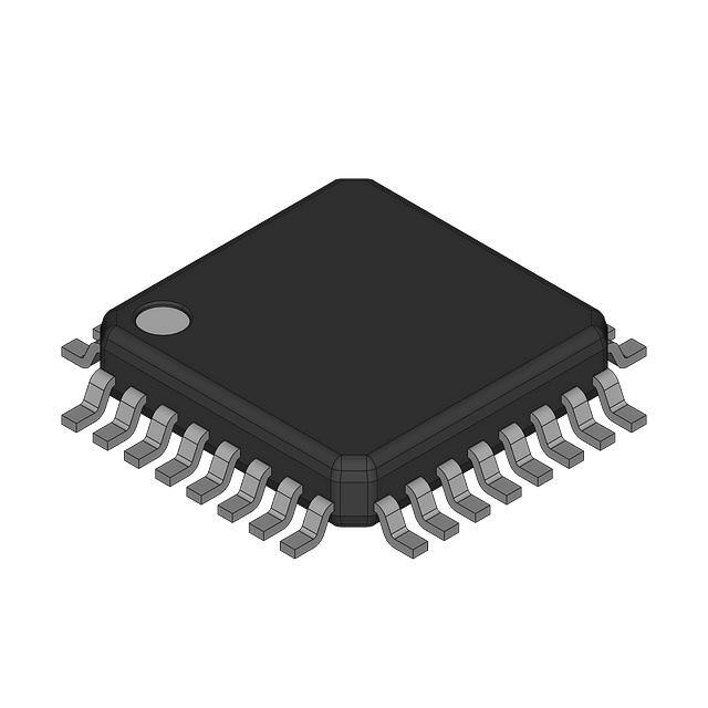


 工商网监
湘ICP备2023018690号
工商网监
湘ICP备2023018690号
