AO7801
Dual P-Channel Enhancement Mode Field Effect Transistor
General Description
Features
The AO7801 uses advanced trench technology to provide
excellent RDS(ON), low gate charge, and operation with gate
voltages as low as 1.8V, in the small SOT363 footprint. It
can be used for a wide variety of applications, including load
switching, low current inverters and low current DC-DC
converters. It is ESD protected to 2KV HBM.
VDS (V) = -20V
ID = -0.6A (VGS = -4.5V)
RDS(ON) < 520mΩ (VGS = -4.5V)
RDS(ON) < 700mΩ (VGS = -2.5V)
RDS(ON) < 950mΩ (VGS = -1.8V)
SC70-6L
(SOT-363)
D2
D1
Pin1
Bottom View
Top View
S1
1
6
D1
G1
2
5
G2
D2
3
4
S2
G2
G1
S2
S1
Pin1
Absolute Maximum Ratings TA=25°C unless otherwise noted
Parameter
Symbol
Drain-Source Voltage
VDS
VGS
Gate-Source Voltage
TA=25°C
Continuous Drain
A
Current
TA=70°C
Pulsed Drain Current
B
TA=25°C
Power Dissipation
A
TA=70°C
Junction and Storage Temperature Range
Thermal Characteristics
Parameter
A
Maximum Junction-to-Ambient
Maximum Junction-to-Ambient A
Maximum Junction-to-Lead C
Rev 3: April 2015
Maximum
-20
Units
V
±8
V
-0.6
ID
-0.48
IDM
-3
A
0.3
PD
W
0.19
TJ, TSTG
-55 to 150
Symbol
t ≤ 10s
Steady-State
Steady-State
RθJA
RθJL
www.aosmd.com
Typ
360
400
300
°C
Max
415
460
350
Units
°C/W
°C/W
°C/W
Page 1 of 5
�Electrical Characteristics (TJ=25°C unless otherwise noted)
Parameter
Symbol
STATIC PARAMETERS
BVDSS
Drain-Source Breakdown Voltage
Conditions
Min
ID=-250µA, VGS=0V
-20
-1
Zero Gate Voltage Drain Current
IGSS
Gate-Body leakage current
VDS=0V, VGS=±8V
VGS(th)
Gate Threshold Voltage
VDS=VGS ID=-250µA
-0.5
ID(ON)
On state drain current
VGS=-4.5V, VDS=-5V
-3
TJ=55°C
µA
V
400
520
542
700
VGS=-2.5V, ID=-0.5A
540
700
mΩ
VGS=-1.8V, ID=-0.4A
700
950
mΩ
TJ=125°C
Forward Transconductance
VDS=-5V, ID=-0.6A
Diode Forward Voltage
IS=-0.5A,VGS=0V
IS
Maximum Body-Diode Continuous Current
DYNAMIC PARAMETERS
Input Capacitance
Ciss
Crss
Reverse Transfer Capacitance
Rg
Gate resistance
Gate Source Charge
A
1.7
-0.86
114
VGS=0V, VDS=-10V, f=1MHz
VGS=-4.5V, VDS=-10V, ID=-0.6A
mΩ
S
-1
V
-0.4
A
140
17
pF
pF
14
VGS=0V, VDS=0V, f=1MHz
SWITCHING PARAMETERS
Total Gate Charge
Qg
Qgs
µA
±10
gFS
Output Capacitance
-5
-0.9
VSD
Coss
Units
-0.6
VGS=-4.5V, ID=-0.6A
Static Drain-Source On-Resistance
Max
V
VDS=-16V, VGS=0V
IDSS
RDS(ON)
Typ
pF
12
17
1.44
1.8
Ω
nC
0.14
nC
Qgd
Gate Drain Charge
0.35
nC
tD(on)
Turn-On DelayTime
6.5
ns
6.5
ns
18.2
ns
VGS=-4.5V, VDS=-10V,
RL=16.7Ω, RGEN=3Ω
tr
Turn-On Rise Time
tD(off)
Turn-Off DelayTime
tf
trr
Turn-Off Fall Time
IF=-0.6A, dI/dt=100A/µs
10
Qrr
Body Diode Reverse Recovery Charge IF=-0.6A, dI/dt=100A/µs
3
Body Diode Reverse Recovery Time
5.5
ns
13
ns
nC
A: The value of R θJA is measured with the device mounted on 1in 2 FR-4 board with 2oz. Copper, in a still air environment with T A =25°C.
The value in any a given application depends on the user's specific board design. The current rating is based on the t ≤ 10s thermal
resistance rating.
B: Repetitive rating, pulse width limited by junction temperature.
C. The R θJA is the sum of the thermal impedence from junction to lead R θJL and lead to ambient.
D. The static characteristics in Figures 1 to 6,12,14 are obtained using 80 µs pulses, duty cycle 0.5% max.
E. These tests are performed with the device mounted on 1 in 2 FR-4 board with 2oz. Copper, in a still air environment with T A=25°C. The
SOA curve provides a single pulse rating.
THIS PRODUCT HAS BEEN DESIGNED AND QUALIFIED FOR THE CONSUMER MARKET. APPLICATIONS OR USES AS CRITICAL
COMPONENTS IN LIFE SUPPORT DEVICES OR SYSTEMS ARE NOT AUTHORIZED. AOS DOES NOT ASSUME ANY LIABILITY ARISING
OUT OF SUCH APPLICATIONS OR USES OF ITS PRODUCTS. AOS RESERVES THE RIGHT TO IMPROVE PRODUCT DESIGN,
FUNCTIONS AND RELIABILITY WITHOUT NOTICE.
Rev 3: April 2015
www.aosmd.com
Page 2 of 5
�TYPICAL ELECTRICAL AND THERMAL CHARACTERISTICS
4
6
-6V
-10V
25°
-4.5V
VDS=-5V
-4V
3
125°C
-3.5V
-ID(A)
-ID (A)
4
-3V
2
-2.5V
2
1
VGS=-2.0V
0
0
0
1
2
3
4
5
0
0.5
-VDS (Volts)
Fig 1: On-Region Characteristics
1.5
2
2.5
3
3.5
4
4.5
-VGS(Volts)
Figure 2: Transfer Characteristics
900
1.6
VGS=-1.8V
Normalized On-Resistance
VGS=-1.8V
800
RDS(ON) (mΩ)
1
700
VGS=-2.5V
600
500
VGS=-4.5V
400
300
ID=-0.4A
1.4
VGS=-2.5V
ID=-0.5A
1.2
VGS=-4.5V
ID=-0.6A
1
0.8
0
1
2
3
4
0
-ID (A)
Figure 3: On-Resistance vs. Drain Current and
Gate Voltage
25
50
75
100
125
150
175
Temperature (°C)
Figure 4: On-Resistance vs. Junction Temperature
1.0E+00
900
ID=-0.6A
800
1.0E-01
1.0E-02
600
-IS (A)
RDS(ON) (mΩ)
125°C
700
125°
500
25°C
1.0E-03
1.0E-04
25°
400
1.0E-05
300
0
2
4
6
8
10
1.0E-06
0.0
-VGS (Volts)
Figure 5: On-Resistance vs. Gate-Source Voltage
Rev 3: April 2015
www.aosmd.com
0.4
0.8
1.2
-VSD (Volts)
Figure 6: Body-Diode Characteristics
Page 3 of 5
�TYPICAL ELECTRICAL AND THERMAL CHARACTERISTICS
200
5
VDS=-10V
ID=-0.6A
Ciss
150
Capacitance (pF)
-VGS (Volts)
4
3
2
100
Coss
50
1
0
0.0
0.5
1.0
1.5
Crss
0
2.0
0
-Qg (nC)
Figure 7: Gate-Charge Characteristics
10µs
100µs
10
10ms
0.1s
1s
10s
20
TJ(Max)=150°
C
12
Power (W)
-ID (Amps)
1ms
0.10
15
14
TJ(Max)=150°C, TA=25°C
1.00
10
-VDS (Volts)
Figure 8: Capacitance Characteristics
10.00
RDS(ON)
limited
5
DC
8
6
4
0.01
2
0
0.001
0.00
0.1
1
10
100
ZθJA Normalized Transient
Thermal Resistance
D=Ton/T
TJ,PK=TA+PDM.ZθJA.RθJA
RθJA=415°C/W
0.1
1
10
100
1000
Pulse Width (s)
Figure 10: Single Pulse Power Rating Junction-toAmbient (Note E)
-VDS (Volts)
Figure 9: Maximum Forward Biased Safe
Operating Area (Note E)
10
0.01
In descending order
D=0.5, 0.3, 0.1, 0.05, 0.02, 0.01, single pulse
1
PD
0.1
Ton
T
Single Pulse
0.01
0.00001
0.0001
0.001
0.01
0.1
1
10
100
1000
Pulse Width (s)
Figure 11: Normalized Maximum Transient Thermal Impedance
Rev 3: April 2015
www.aosmd.com
Page 4 of 5
�Gate Charge Test Circuit & Waveform
Vgs
Qg
10V
+
+ Vds
VDC
-
Qgs
Qgd
VDC
-
DUT
Vgs
Ig
Charge
Resistive Switching Test Circuit & W aveform s
RL
Vds
Vds
DUT
Vgs
90%
+ Vdd
VDC
-
Rg
10%
Vgs
Vgs
t d(on)
tr
t d(off)
t on
tf
t off
Diode Recovery Test Circuit & Waveforms
Q rr = - Idt
Vds +
DUT
Vds -
Isd
Vgs
Ig
Rev 3: April 2015
Vgs
L
Isd
+ Vdd
t rr
dI/dt
I RM
Vdd
VDC
-
IF
Vds
www.aosmd.com
Page 5 of 5
�
很抱歉,暂时无法提供与“AO7801”相匹配的价格&库存,您可以联系我们找货
免费人工找货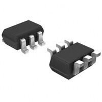


 工商网监
湘ICP备2023018690号
工商网监
湘ICP备2023018690号
