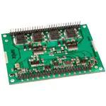
MSA260
MSA260
MSA260
Pulse Width Modulation Amplifier
FEATURES
GENERAL DESCRIPTION
The MSA260 is a surface mount constructed PWM
amplifier that provides a cost effective solution in many
industrial applications. The MSA260 offers outstanding performance that rivals many much more expensive hybrid components. The MSA260 is a complete
PWM amplifier including an oscillator, comparator, error amplifier, current limit comparators, 5V reference,
a smart controller and a full bridge IGBT output circuit.
The switching frequency is user programmable up to
50 kHz. The MSA260 is built on a thermally conductive
but electrically insulating substrate that can be mounted to a heatsink.
• LOW COST
• HIGH VOLTAGE - 450 VOLTS
• HIGH OUTPUT CURRENT - 20 AMPS
• 9kW OUTPUT CAPABILITY
• VARIABLE SWITCHING FREQUENCY
• IGBT FULL BRIDGE OUTPUT
APPLICATIONS
• BRUSH MOTOR CONTROL
• MRI
• MAGNETIC BEARINGS
• CLASS D SWITCHMODE AMPLIFIER
EQUIVALENT CIRCUIT DIAGRAM
VCC
29
5V REF
OUT
19
SIGNAL
GND
26
2
SIGNAL
GND
SIGNAL
GND
23
DIGITAL
RETURN
18
ILIM B
5V
REF
7
30-34
+Vs
ROSC
22
CLK OUT
Q2
+
35-39
-
2.68K
2200pF
Q1
-
1K
10
+Vs
+
1K
.01µF
ILIM A/
SHDN
44-48
200mV
A OUT
SMART
CONTROLLER
.01µF
Q3
OSC
49-53
24
B OUT
Q4
E/A OUT
17
E/A -IN
16
-
E/A +IN
15
+
+IN
13
RRAMP IN
20
CLK IN
21
AC BACK
PLATE
28
APEX TP
27
PWR
GND
58
www.apexanalog.com
MSA260U
I SENSE B
R2
+
R3
5.36K
1
CLK/2 OUT
54-57
40-43
I SENSE A
-
2200pF
CLK/2
BACK PLATE
1µF
Copyright © Apex Microtechnology, Inc. 2014
(All Rights Reserved)
JUL 2014
1
MSA260U REVF
�MSA260
CHARACTERISTICS AND SPECIFICATIONS
ABSOLUTE MAXIMUM RATINGS
Parameter
Symbol
Min
Max
Units
SUPPLY VOLTAGE
VS
450
V
SUPPLY VOLTAGE
VCC
16
V
OUTPUT CURRENT, peak, within SOA
POWER DISSIPATION, internal, DC
(Note 3)
SIGNAL INPUT VOLTAGES
TEMPERATURE, pin solder, 10s
TEMPERATURE, junction
(Note 2)
30
A
250
W
5.4
V
225
°C
150
°C
TEMPERATURE RANGE, storage
−40
105
°C
OPERATING TEMPERATURE, case
−40
85
°C
SPECIFICATIONS
Parameter
Test Conditions (Note 1)
Min
Typ
Max
Units
Full temperature range
9
mV
ERROR AMPLIFIER
OFFSET VOLTAGE
BIAS CURRENT, initial
Full temperature range
500
nA
OFFSET CURRENT, initial
(Note 3)
Full temperature range
150
nA
COMMON MODE VOLTAGE RANGE, pos.
Full temperature range
4
V
SLEW RATE
Full temperature range
1
V/µs
OPEN LOOP GAIN
RL = 2KΩ
96
dB
1
MHz
0
UNITY GAIN BANDWIDTH
CLOCK
LOW LEVEL OUTPUT VOLTAGE
Full temperature range
HIGH LEVEL OUTPUT VOLTAGE
Full temperature range
0.2
4.8
V
V
RISE TIME
7
nS
FALL TIME
7
nS
BIAS CURRENT, pin 22
Full temperature range
0.6
µA
5.15
V
2
mA
2.25
V
5V REFERENCE OUTPUT
VOLTAGE
4.85
LOAD CURRENT
OUTPUT
(Note 4)
VCE(ON), each active IGBT
ICE = 15A
CURRENT, continuous
VS = 400V, F = 22kHz
20
A
CURRENT, peak
1mS, VS = 400V, F = 22kHz
30
A
FLYBACK DIODE
CONTINUOUS CURRENT
FORWARD VOLTAGE
IF = 15A
REVERSE RECOVERY
IF = 15A
2
0.2
44
20
A
200
1.5
V
0.7
150
nS
MSA260U
�MSA260
Parameter
Test Conditions (Note 1)
Min
Typ
Max
Units
5
400
450
V
14
15
16
V
9
28
mA
18
mA
10
mA
1
°C/W
14
°C/W
85
°C
POWER SUPPLY
VOLTAGE, VS
VOLTAGE, VCC
CURRENT, VS, quiescent
22kHz switching
CURRENT, VCC, quiescent
22kHz switching
CURRENT, VCC, shutdown
THERMAL
RESISTANCE, DC, junction to case
Full temperature range
RESISTANCE, junction to air
Full temperature range
TEMPERATURE RANGE, case
-40
50
EACH ACTIVE
COMPONENT
25
0
20
40
60
80
100
CASE TEMPERATURE, (C)
REVERSE DIODE
TJ =
125
C
16
12
8
4
0
0.4
0.6
0.8
1.0
SOURCE TO DRAIN DIODE VOLTAGE
25
99
98
FREQUENCY = 44KHz
97
1M
100K
10K
CLOCK LOAD RESISTANCE, ()
TC
3
5
=
99.4
99.2
-40 -20
0 20 40 60 80 100
CASE TEMPERATURE, (C)
85
TC
5C
=2
2
4
8
12
16
OUTPUT CURRENT, (A)
20
VCC QUIESCENT CURRENT
DUTY CYCLE VS. ANALOG INPUT
100
DUTY CYCLE, (%)
CONTINUOUS AMPS
10
MSA260U
99.6
C
A OUT
15
99.8
TOTAL VOLTAGE DROP
4
1
0
CONTINUOUS OUTPUT
20
CLOCK FREQUENCY OVER TEMP.
100.2
100.0
5
TOTAL VOLTAGE DROP, (V)
0
CLOCK LOADING
NORMALIZED FREQUENCY, (%)
75
100
80
60
40
20
B OUT
QUIESCENT CURRENT, (mA)
100
20
FLYBACK CURRENT, ISD (A)
NORMALIZED FREQUENCY, (%)
POWER DERATING
125
TJ =
25C
INTERNAL POWER DISSIPATION, (W)
NOTES:
1. Unless otherwise noted: TC=25°C, VCC = 15V, VS = 400V, F = 22kHz.
2. Long term operation at the maximum junction temperature will result in reduced product life. Derate
internal power dissipation to achieve high MTBF.
3. Each of the two output transistors on at any one time can dissipate 125W.
4. Maximum specification guaranteed but not tested.
24
20
16
12
8
3
50% DUTY CYCLE
�TOTAL VOLTAGE D
4
MSA260
TC
3
85
TC
5C
=2
2
0
0.4
0.6
0.8
1.0
SOURCE TO DRAIN DIODE VOLTAGE
1
0
4
8
12
16
OUTPUT CURRENT, (A)
20
VCC QUIESCENT CURRENT
DUTY CYCLE VS. ANALOG INPUT
CONTINUOUS OUTPUT
25
=
100
80
DUTY CYCLE, (%)
CONTINUOUS AMPS
A OUT
20
15
10
60
40
20
5
B OUT
0
1.5
100
2.5
3.0
16
12
8
10
101
100
99
NORMAL or SHUTDOWN
OPERATION
97
-40 -20 0 20 40 60 80 100
CASE TEMPERATURE, (C)
VS QUIESCENT CURRENT
VS QUIESCENT CURRENT vs. FREQUENCY
8
6
4
F = 22kHz,
50% DUTY CYCLE
2
0
100
200 300
VS, (V)
400
50% DUTY CYCLE
4
0
10
20
30
40
50
SWITCHING FREQUENCY, F (kHz)
3.5
ANALOG INPUT, (V)
VCC QUIESCENT CURRENT
98
2.0
20
24
VS QUIESCENT CURRENT, IQ (mA)
102
25
50
75
CASE TEMPERATURE, (C)
VS QUIESCENT CURRENT, (mA)
NORMALIZED QUIESCENT CURRENT, (%)
0
0
24
VCC QUIESCENT CURRENT, (mA)
8
TJ =
25C
TJ =
125
C
FLYBACK CURREN
12
500
20
16
12
8
VS = 400V,
50% DUTY CYCLE
4
0
0
10
20
30
40
50
SWITCHING FREQUENCY, F (kHz)
10 11 12 13 14 15 16 17 18 19
NC
SIG GND
APEX TP
AC BACK
PLATE
CLK OUT
DIG RTN
CLK/2 OUT
CLK IN
ROSC
SIG GND
+5V OUT
EA -IN
EA OUT
NC
EA +IN
+IN
9
NC
8
NC
7
ILIM A/SHDN
6
NC
5
ILIM B
4
NC
3
NC
NC
2
NC
SIG GND
1
NC
RRAMP IN
EXTERNAL CONNECTIONS
20 21 22 23 24 25 26 27 28
RRAMP
VIEW FROM
COMPONENT SIDE
C1
58
PWR
GND
4
ROSC
C2
+
C3
57 56 55 54 53 52 51 50 49 48 47 46 45 44 43 42 41 40 39 38 37 36
ISENSE B
B OUT
+Vs
SINGLE
POINT
GND
ISENSE A
A OUT
35 34 33 32 31
+Vs
30 29
VCC
NOTES: C2 IS ELECTROLYTIC ≥10UF PER AMP OUTPUT CURRENT
C1,3 HIGH QUALITY CERAMIC ≥1.0UF
ALL +Vs MUST BE TIED TOGETHER
ALL SIG GND PINS MUST BE TIED TOGETHER
SINGLE POINT GROUND @ PIN 26
MSA260U
�MSA260
58-pin DIP
PACKAGE STYLE KC
TYPICAL APPLICATION
TORQUE MOTOR CONTROL
With the addition of a few external components the MSA260 becomes a motor torque controller.
In the MSA260 the source terminal of each low side IGBT driver
is brought out for current sensing
via RSA and RSB. A1 is a differential amplifier that amplifies the difference in currents of the two half
bridges. This signal is fed into the
internal error amplifier that mixes
the current signal and the control
signal. The result is an input signal to the MSA260 that controls
the torque on the motor.
SINGLE POINT GND @ 26
20
RRAMP
58
2,18,26
28
23
SIG DIG PWR
AC
GND RET GND
BACK
PLATE
CLK/2 OUT
1
RRAMP IN
21 CLK IN
24
CLK OUT
ROSC
22 ROSC
A OUT
35-39
PWM AMPLIFIER
19 +5V REF OUT
13 +IN
17 E/A OUT
B OUT
49-53
16 E/A -IN
15 E/A +IN
CONTROL
SIGNAL
Is B
Is A
54-57
2.5V
40-43
A1
Rs A
Rs B
2.5V
GENERAL
Please read Application Note 30 “PWM Basics”. Refer also to Application Note 1 “General Operating Considerations” for helpful information regarding power supplies, heat sinking, mounting, SOA interpretation, and specification interpretation. Visit www.apexanalog.com for design tools that help automate tasks such as calculations for
stability, internal power dissipation, current limit, heat sink selection, Apex Microtechnology’s complete Application
Notes library, Technical Seminar Workbook and Evaluation Kits.
MSA260U
5
�MSA260
OSCILLATOR
The MSA260 includes a user frequency programmable oscillator. The oscillator determines the switching frequency
of the amplifier. The switching frequency of the amplifier is 1/2 the oscillator frequency. Two resistor values must
be chosen to properly program the switching frequency of the amplifier. One resistor, ROSC, sets the oscillator frequency. The other resistor, RRAMP, sets the ramp amplitude. In all cases the ramp voltage will oscillate between 1.5V
and 3.5V. See Figure 1. If an external oscillator is applied use the equations to calculate RRAMP .
RRAMP = 2 X ROSC
Use 1% resistors with 100ppm drift (RN55C type resistors,
for example). Maximum switching frequency is 50kHz.
PWR
GND
58
10
7
Isense B
where F is the desired switching frequency and:
Isense A
ROSC = (1.32X10⁸ / F) - 2680
IlimB
PWM AMPLIFIER
IlimA/SHDN
To program the oscillator, ROSC is given by:
40-43
R
54-57
C
9R
R
Example:
C
If the desired switching frequency is 22kHz then ROSC =
Rs A
Rs B
5V SHDN
3.32K and RRAMP = 6.64K. Choose the closest standard 1%
SIGNAL
values: ROSC = 3.32K and RRAMP = 6.65K or simply use two
of selected ROSC in series for RRAMP.
FIGURE 1. EXTERNAL OSCILLATOR CONNECTIONS
21
20
CLK/2 OUT
24
CLK IN
22
RRAMP
CLK OUT
CURRENT SENSING
ROSC
ROSC
The MSA260 output stage can be turned off with a shutdown command voltage applied to Pin 10 as shown in Figure 2. The shutdown signal is OR’ed
with the current limit signal and simply overrides it. As long as the shutdown
signal remains high the output will be off.
1
RRAMP IN
SHUTDOWN
The low side drive transistors of the MSA260 are brought out for sensing the
PWM AMPLIFIER
current in each half bridge. A resistor from each sense line to PWR GND (pin
58) develops the current sense voltage. Choose R and C such that the time FIGURE 2. CURRENT LIMIT WITH
constant is equal to 10 periods of the selected switching frequency. The in- OPTIONAL SHUTDOWN
ternal current limit comparators trip at 200mV. Therefore, current limit occurs
at I = 0.2/RSENSE for each half bridge. See Figure 2. Accurate milliohm power resistors are required and there are
several sources for these listed in the Accessories Vendors section of the Databook.
POWER SUPPLY BYPASSING
Bypass capacitors to power supply terminals +VS must be connected physically close to the pins to prevent local
parasitic oscillation and overshoot. All +VS must be connected together. Place and electrolytic capacitor of at least
10µF per output amp required midpoint between these sets of pins. In addition place a ceramic capacitor 1.0µF or
greater directly at each set of pins for high frequency bypassing. VCC is bypassed internally.
GROUNDING AND PCB LAYOUT
Switching amplifiers combine millivolt level analog signals and large amplitude switching voltages and currents with
fast rise times. As such grounding is crucial. Use a single point ground at SIG GND (pin 26). Connect signal ground
pins 2 and 18 directly to the single point ground on pin 26. Connect the digital return pin 23 directly to pin 26 as well.
Connect PWR GND pin 58 also to pin 26. Connect AC BACKPLATE pin 28 also to the single point ground at pin 26.
Connect the ground terminal of the VCC supply directly to pin 26 as well. Make sure no current from the load return
to PWR GND flows in the analog signal ground. Make sure that the power portion of the PCB layout does not pass
over low-level analog signal traces on the opposite side of the PCB. Capacitive coupling through the PCB may inject
switching voltages into the analog signal path. Further, make sure that the power side of the PCB layout does not
come close to the analog signal side. Fast rising output signal can couple through the trace-to-trace capacitance on
the same side of the PCB.
6
MSA260U
�MSA260
DETERMINING THE OUTPUT STATE
The input signal is applied to +IN (Pin 13) and varies from 1.5 to 3.5 volts, zero to full scale. The ramp also varies
over the same range. When:
Ramp > +IN AOUT > BOUT
The output duty cycle extremes vary somewhat with switching frequency and are internally limited to approximately
5% to 95% at 10kHz and 7% to 93% at 50kHz.
CALCULATING INTERNAL POWER DISSIPATION
Detailed calculation of internal power dissipation is complex but can be approximated with simple equations. Conduction loss is given by:
W = I • 2.5 + I2 • 0.095
where I = output current
Switching loss is given by:
W = 0.00046 • I • Vsupply • Fswitching (in kHz)
Combine these two losses to obtain total loss. Calculate heatsink ratings and case temperatures as would be done
for a linear amplifier. For calculation of junction temperatures, assume half the loss is dissipated in each of two
switches:
Tj = Ta + Wtotal • RØhs + 1/2Wtotal • RØjc, where:
RØhs = heatsink rating
RØjc = junction-to-case thermal resistance of the MSA260.
The SOA typical performance graphs below show performance with the MSA260 mounted with thermal grease on
the Apex Microtechnology HS26. The Free Air graph assumes vertical orientation of the heatsink and no obstruction to air flow in an ambient temperature of 30°C. The other two graphs show performance with two levels of forced
air. Note that air velocity is given in linear feet per minute. As fans are rated in cubic delivery capability, divide the
cubic rating by the square area this air flows through to find velocity. As fan delivery varies with static pressure,
these calculations are approximations, and heatsink ratings vary with amount of power dissipated, there is no substitute for temperature measurements on the heatsink in the center of the amplifier footprint as a final check.
SOA, HS26, FREE AIR
SOA, HS26, 150LFM FORCED AIR
150
Vs
=2
Vs
50
Vs
=3
=4
50
50
18
16
14
MSA260U
Vs=350
12
10
7
5 10 15 20 25 30 35 40 45 50
SWITCHING FREQUENCY, KHz
Vs=250
Vs=450
5 10 15 20 25 30 35 40 45 50
SWITCHING FREQUENCY, KHz
19
OUTPUT CURRENT, A
Vs=
16
10
20
Vs=150
OUTPUT CURRENT, A
OUTPUT CURRENT, A
19
13
SOA, HS26, 500LFM FORCED AIR
20
Vs=250
18
17
Vs=350
16
15
Vs=450
14
13
12
15 20 25 30 35 40 45 50
SWITCHING FREQUENCY, KHz
7
�MSA260
NEED TECHNICAL HELP? CONTACT APEX SUPPORT!
For all Apex Microtechnology product questions and inquiries, call toll free 800-546-2739 in North America.
For inquiries via email, please contact apex.support@apexanalog.com.
International customers can also request support by contacting their local Apex Microtechnology Sales Representative.
To find the one nearest to you, go to www.apexanalog.com
IMPORTANT NOTICE
Apex Microtechnology, Inc. has made every effort to insure the accuracy of the content contained in this document. However, the information is subject to change
without notice and is provided "AS IS" without warranty of any kind (expressed or implied). Apex Microtechnology reserves the right to make changes without further
notice to any specifications or products mentioned herein to improve reliability. This document is the property of Apex Microtechnology and by furnishing this information, Apex Microtechnology grants no license, expressed or implied under any patents, mask work rights, copyrights, trademarks, trade secrets or other intellectual
property rights. Apex Microtechnology owns the copyrights associated with the information contained herein and gives consent for copies to be made of the information only for use within your organization with respect to Apex Microtechnology integrated circuits or other products of Apex Microtechnology. This consent does not
extend to other copying such as copying for general distribution, advertising or promotional purposes, or for creating any work for resale.
APEX MICROTECHNOLOGY PRODUCTS ARE NOT DESIGNED, AUTHORIZED OR WARRANTED TO BE SUITABLE FOR USE IN PRODUCTS USED FOR
LIFE SUPPORT, AUTOMOTIVE SAFETY, SECURITY DEVICES, OR OTHER CRITICAL APPLICATIONS. PRODUCTS IN SUCH APPLICATIONS ARE UNDERSTOOD TO BE FULLY AT THE CUSTOMER OR THE CUSTOMER’S RISK.
Apex Microtechnology, Apex and Apex Precision Power are trademarks of Apex Microtechnolgy, Inc. All other corporate names noted herein may be trademarks
of their respective holders.
www.apexanalog.com
8
Copyright © Apex Microtechnology, Inc. 2014
(All Rights Reserved)
JUL 2014
MSA260U
MSA260U REVF
�


 工商网监
湘ICP备2023018690号
工商网监
湘ICP备2023018690号
