ASMT-Mx00
MoonstoneTM 1 W Power LED Light Source
Data Sheet
Description
Features
The Moonstone 1W Power LED Light Source is a high
performance energy efficient device which can handle
high thermal and high driving current. The exposed pad
design has excellent heat transfer from the package to
the motherboard.
TM
The Cool White Power LED is available in various color
temperature ranging from 4000K to 10000K and Warm
White Power LED ranging from 2600K to 4000K.
The low profile package design is suitable for a wide
variety of applications especially where height is a
constraint.
The package is compatible with reflow soldering
process. This will give more freedom and flexibility to
the light source designer.
Applications
• Portable (flash light, bicycle head light)
• Reading light
• Architectural lighting
• Garden lighting
• Decorative lighting
• Available in Red, Amber, Green, Blue, Cool White and
Warm White color
• Energy efficient
• Exposed pad for excellent heat transfer
• Suitable for reflow soldering process
• High current operation
• Long operation life
• Wide viewing angle
• Silicone encapsulation
• ESD Class HBM Class 3B (threshold > 8 kV)
• MSL 2A for InGaN products
• MSL 4 for AlInGaP products
Specifications
• AlInGaP technology for Red and Amber
• 2.4 V (typ) at 350 mA for AlInGaP
• InGaN technology for Green, Blue, Cool White and
Warm White
• 3.6 V (typ) at 350 mA for InGaN
• 120 viewing angle
�Package Dimensions
10.00
1
Anode
2 Cathode
3
Heat Sink
3.30
8.50
1.27
Metal Slug
3
Ø 5.26
LED
10.60
+
−
8.50
ZENER
Ø 8.00
2.00
5.25
1.30
2
1
5.08
0.81
Notes:
1. All dimensions are in millimeters.
2. Tolerance is ±0.1 mm unless otherwise specified.
3. Metal slug is connected to anode for electrically non-isolated option.
Device Selection Guide ( Tj = 25°C)
Luminous Flux, fV[1,2] (lm)
Part Number
Color
Min.
Typ.
Max.
Test Current
(mA)
Dice
Technology
ASMT-MR00-AGH00
Red
25.5
35.0
43.0
350
AlInGaP
33.0
40.0
56.0
350
AlInGaP
ASMT-MR00-AHJ00
ASMT-MA00-AGH00
Amber
25.5
35.0
43.0
350
AlInGaP
ASMT-MG00
Green
43.0
60.0
73.0
350
InGaN
ASMT-MB00
Blue
11.5
15.0
25.5
350
InGaN
ASMT-MW00
Cool White
43.0
60.0
73.0
350
InGaN
ASMT-MY00
Warm White
43.0
50.0
73.0
350
InGaN
ASMT-MWB1
Cool White Diffused
43.0
55.0
73.0
350
InGaN
ASMT-MYB1
Warm White Diffused
43.0
46.0
73.0
350
InGaN
Notes
1. fV is the total luminous flux output as measured with an integrating sphere at 25 ms mono pulse condition.
2. Flux tolerance is ± 10%.
2
�Part Numbering System
ASMT-M x xx – x x1 x2 x3 x4
Packaging Option
Color Bin Selection
Maximum Flux Bin Selection
Minimum Flux Bin Selection
Dice Type
N – InGaN
A – AllnGaP
Silicone Type
00 – Non-diffused
B1 – Diffused
Color
R – Red
A – Amber
G - Green
B - Blue
W - Cool White
Y - Warm White
Note:
1. Please refer to Page 8 for selection details.
Absolute Maximum Ratings (TA = 25°C)
Parameter
ASMT-Mx00 / ASMT-MxB1
Units
350
mA
1000
mA
Power Dissipation for AlInGaP
1050
mW
Power Dissipation for InGaN
1400
mW
LED Junction Temperature for AlInGaP
125
°C
LED Junction Temperature for InGaN
110
°C
Operating Ambient Temperature Range
-40 to +100
°C
Storage Temperature Range
-40 to +120
°C
DC Forward Current
[1]
Peak Pulsing Current
[2]
Notes:
1. DC forward current – derate linearly based on Figure 5 for AlInGaP & Figure 11 for InGaN.
2. Pulse condition duty factor = 10%, Frequency = 1kHz.
3
�Optical Characteristics at 350 mA (TJ = 25°C)
Dominant
Wavelength
lD [1] (nm)
Typ.
Viewing Angle
2q1/2 [2] (°)
Typ.
Luminous
Efficiency (lm/W)
Typ.
Part Number
Color
Peak Wavelength
lPEAK (nm)
Typ.
ASMT-MR00-AGH00
Red
635
625
120
42
ASMT-MR00-AHJ00
Red
635
625
120
48
ASMT-MA00-AGH00
Amber
598
590
120
42
ASMT-MG00
Green
519
525
120
48
ASMT-MB00
Blue
460
467
120
12
Correlated Color Temperature,
CCT (Kelvin)
Viewing Angle
2q½ [2] (°)
Luminous
Efficiency (lm/W)
Part Number
Color
Min.
Max.
Typ.
Typ.
ASMT-MW00
Cool White
4000
10000
110
48
ASMT-MY00
Warm White
2600
4000
110
40
ASMT-MWB1
Cool White Diffused
4000
10000
110
44
ASMT-MYB1
Warm White Diffused
2600
4000
110
37
Notes:
1. The dominant wavelength, λD, is derived from the CIE Chromaticity Diagram and represents the color of the device.
2. θ1/2 is the off-axis angle where the luminous intensity is 1/2 the peak intensity.
Electrical Characteristic at 350 mA (TJ = 25°C)
Forward Voltage
VF (Volts) at IF = 350mA
Reverse Voltage
VR (Volts)
Thermal Resistance
Rqj-ms (°C/W) [1]
Dice Type
Min
Typ.
Max.
Max.
Typ.
AlInGaP
2.0
2.4
3.0
5
12
InGaN
3.2
3.6
4.0
5
10
Notes:
1. RqJ-ms is Thermal Resistance from LED junction to metal slug.
4
�RED
AMBER
FORWARD CURRENT - mA
RELATIVE INTENSITY
1.0
0.9
0.8
0.7
0.6
0.5
0.4
0.3
0.2
0.1
0.0
380
430
480
530
580
630
WAVELENGTH - nm
680
730
780
Figure 1. Relative Intensity vs. Wavelength for AlInGaP
500
450
400
350
300
250
200
150
100
50
0
0.00
1.0
RELATIVE INTENSITY
RELATIVE LUMINOUS FLUX (-v) - lm
1.2
0.8
0.6
0.4
0.2
0
50
100
150 200 250 300 350 400
MONO PULSE CURRENT - mA
450 500
Figure 3. Relative Luminous Flux vs. Mono Pulse Current for AlInGaP
RELATIVE LOP (Normalized at 25°C)
I F - MAX FORWARD CURRENT - mA
3.00
1
0.9
0.8
0.7
0.6
0.5
0.4
0.3
0.2
0.1
0
-90
-70
-50
-30
-10
10
30
OFF-AXIS ANGLE(°)
50
70
90
2
350
R JA = 60°C/W
300
R JA = 50°C/W
250
R JA = 40°C/W
200
150
100
50
0
10
20
30
40
50
60
T A - AMBIENT TEMPERATURE - °C
70
80
90
Figure 5. Maximum forward current vs. ambient temperature for AlInGaP
Derated based on TJMAX = 125°C, RθJA = 40°C/W / 50°C/W and 60°C/W
5
2.50
Figure 4. Radiation Pattern for AlInGaP
400
0
1.00
1.50
2.00
FORWARD VOLTAGE - V
Figure 2. Forward Current vs Forward Voltage for AlInGaP
1.4
0.0
0.50
RED
AMBER
1.5
1
0.5
0
-40 -25 -10
5
20 35 50 65 80
JUNCTION TEMPERATURE - °C
95 110 125
Figure 6. Relative LOP (Normalized at 25°C) vs. junction temperature for
AlInGaP
�GREEN
BLUE
COOL WHITE
WARM WHITE
430
480
530
580
630
WAVELENGTH - nm
680
730
FORWARD CURRENT - mA
RELATIVE INTENSITY
1.0
0.9
0.8
0.7
0.6
0.5
0.4
0.3
0.2
0.1
0.0
380
780
1.2
1.0
RELATIVE INTENSITY
RELATIVE LUMINOUS FLUX (φV) - lm
1.4
0.8
0.6
0.4
0.2
0
50
100 150 200 250 300 350 400 450 500
MONO PULSE CURRENT - mA
540
350
530
RθJA = 50 C/W
RθJA = 40 C/W
200
RθJA = 30 C/W
150
100
50
0
0
10
20
30
40
50
60
70
T A – AMBIENT TEMPERATURE – °C
80
90
Figure 11. Maximum Forward Current vs. Ambient Temperature for InGaN
Derated based on TJMAX = 110°C, RθJA = 30°C/W, 40°C/W and 50°C/W
6
1.0
0.9
0.8
0.7
0.6
0.5
0.4
0.3
0.2
0.1
0.0
-90
400
250
1.00
1.50 2.00 2.50 3.00
FORWARD VOLTAGE - V
3.50
4.00
70
90
GREEN
BLUE
COOL WHITE
WARM WHITE
-70
-50
-30
-10 10
30
OFF-AXIS ANGLE (°)
50
Figure 10. Radiation Pattern for InGaN
DOMINANT WAVELENGTH – nm
I F – MAXIMUM FORWARD CURRENT – mA
Figure 9. Relative Luminous Flux vs Mono Pulse Current for InGaN
300
0.50
Figure 8. Forward Current vs. Forward Voltage for InGaN
Figure 7. Relative Intensity vs. Wavelength for InGaN
0.0
500
450
400
350
300
250
200
150
100
50
0
0.00
GREEN
520
510
500
490
480
BLUE
470
460
450
100
150
200
250
300
FORWARD CURRENT – mA
350
Figure 12. Dominant wavelength vs. forward current – InGaN devices
400
�0.016
100 mA
0.014
150 mA
Y-COORDINATES
0.012
0.01
0.008
250 mA
0.006
0.004
300 mA
0.002
0
0
350 mA
0.001 0.002 0.003 0.004 0.005 0.006 0.007 0.008
X-COORDINATES
Figure 13. Chromaticity shift vs. current
*Note: (x,y) values @ 350 mA reference to (0.0)
10.70 ± 0.10
TEMPERATURE
10 - 30 SEC.
217 °C
200 °C
255 - 260 °C
3 °C/SEC. MAX.
8.40 ± 0.10
-6 °C/SEC. MAX.
17.00 ± 0.20
150 °C
3 °C/SEC. MAX.
1.00 ± 0.10
60 - 120 SEC.
(Acc. to J-STD-020C)
100 SEC. MAX.
3.1 ± 0.10
5.08 ± 0.10
TIME
300
250
200
150
100
50
0
-50
-100
-150
-200
-250
-300
-40
Figure 15. Recommended soldering land pattern
100
90
80
70
60
50
40
30
20
10
0
25 30 35 40 45 50 55 60 65 70 75 80 85 90
JUNCTION TEMPERATURE (°C)
RELATIVE LOP (%)
RELATIVE FORWARD VOLTAGE SHIFT (mV)
Figure 14. Recommended reflow soldering profile
-15
10
35
TEMPERATURE - °C
Figure 16. Temperature vs. relative forward voltage shift
60
85
GREEN
BLUE
COOL WHITE
WARM WHITE
95 100105110
Figure 17. Relative LOP vs Junction Temperature for InGaN Devices
Note:
For detail information on reflow soldering of Avago surface mount LEDs, do refer to Avago Application Note AN1060 Surface Mounting SMT LED
Indicator Components.
7
�Option Selection Details
ASMT-Mxxx – x x1 x2 x3 x4
x1 – Minimum Flux Bin Selection
x2 – Maximum Flux Bin Selection
x3 – Color Bin Selection
x4 – Packaging Option
Flux Bin Limit [x1 x2]
Bin
Luminous Flux (lm) at IF = 350mA
Min.
Max.
D
11.5
15.0
E
15.0
19.5
F
19.5
25.5
G
25.5
33.0
H
33.0
43.0
J
43.0
56.0
K
56.0
73.0
Tolerance for each bin limits is ±10%
Color Bin Selection [x3]
Individual reel will contain parts from one full bin only.
Cool White
Warm White
0
Full Distribution
0
Full Distribution
A
A only
A
A only
B
B only
B
B only
C
C only
C
C only
D
D only
D
D only
E
E only
E
E only
F
F only
F
F only
N
A and C only
G
G only
P
B and D only
H
H only
Q
E and C only
L
A and G only
R
F and D only
M
B and H only
U
E and F only
N
A and C only
W
C and D only
P
B and D only
Z
A and B only
Q
E and C only
1
A, B, C and D only
R
F and D only
4
C, D, E and F only
S
G and H only
U
E and F only
W
C and D only
Other Colors
0
Full Distribution
Z
A and B only
Z
A and B
1
A, B, C and D only
Y
B and C
2
G, H, A and B only
W
C and D
4
C, D, E and F only
V
D and E
Q
A, B and C
P
B, C and D
N
C, D and E
8
�0.44
0.48
0.42
0.46
0.40
G
A
0.36
C
0.34
5.6k
0.32
4.0k
4.5k
H
7k D
E
0.30
B
0.44
Y - COORDINATE
Y - COORDINATE
0.38
Black Body Curve
0.40
E
0.38
3.5k
D
4.0k
F
2.6k
3.0k
B
Black Body Curve
0.34
0.26
0.24
0.24
C
0.36
10k F
0.28
A
0.42
0.26
0.28
0.30
0.32 0.34 0.36
X - COORDINATE
0.38
0.40
0.42
0.44
0.32
0.34
0.36
0.38
0.40
0.42
0.44
X - COORDINATE
0.46
0.48
0.50
Figure 19. Color bins (Warm White).
Figure 18. Color bins (Cool White).
Color Bin Limits
Warm
White
Color Limits
(Chromaticity Coordinates)
Cool
White
Color Limits
(Chromaticity Coordinates)
Bin A
x
y
0.452
0.434
0.488
0.447
0.470
0.414
0.438
0.403
Bin A
x
y
0.367
0.400
0.362
0.372
0.329
0.345
0.329
0.369
Bin B
x
y
0.438
0.403
0.470
0.414
0.452
0.384
0.424
0.376
Bin B
x
y
0.362
0.372
0.356
0.330
0.329
0.302
0.329
0.345
Bin C
x
y
0.407
0.393
0.418
0.422
0.452
0.434
0.438
0.403
Bin C
x
y
0.329
0.369
0.329
0.345
0.305
0.322
0.301
0.342
Bin D
x
y
0.395
0.362
0.407
0.393
0.438
0.403
0.424
0.376
Bin D
x
y
0.329
0.345
0.329
0.302
0.311
0.285
0.305
0.322
Bin E
x
y
0.381
0.377
0.387
0.404
0.418
0.422
0.407
0.393
Bin E
x
y
0.303
0.333
0.307
0.311
0.283
0.284
0.274
0.301
Bin F
x
y
0.373
0.349
0.381
0.377
0.407
0.393
0.395
0.362
Bin F
x
y
0.307
0.311
0.311
0.285
0.290
0.265
0.283
0.284
Bin G
x
y
0.388
0.417
0.379
0.383
0.362
0.372
0.367
0.400
Bin H
x
y
0.379
0.383
0.369
0.343
0.356
0.330
0.362
0.372
Tolerance: ± 0.01
Color
Bin
Min.
Max.
Red
Full Distribution
620.0
635.0
Amber
A
582.0
584.5
B
584.5
587.0
C
587.0
589.5
D
589.5
592.0
E
592.0
594.5
A
460.0
465.0
B
465.0
470.0
C
470.0
475.0
D
475.0
480.0
A
515.0
520.0
B
520.0
525.0
C
525.0
530.0
D
530.0
535.0
Blue
Green
Tolerance: ± 1 nm
9
Tolerance: ± 0.01
0.52
�Sub-Color Binning
(Only Applicable for Color Bin A to Bin D and Bin G to Bin H)
Color Limits
Cool White
(Chromaticity Coordinates)
Bin A1
X
Y
X
Y
X
Y
X
Y
X
Y
X
Y
X
Y
X
Y
X
Y
X
Y
X
Y
X
Y
X
Y
X
Y
Bin A2
Bin A3
Bin A4
Bin B1
Bin B2
Bin B3
Bin B4
Bin B5
Bin B6
Bin C1
Bin C2
Bin C3
Bin C4
0.364
0.383
0.364
0.383
0.329
0.357
0.329
0.345
0.362
0.372
0.360
0.357
0.358
0.343
0.329
0.331
0.329
0.331
0.343
0.331
0.329
0.369
0.329
0.357
0.314
0.355
0.315
0.344
0.367
0.400
0.362
0.372
0.329
0.369
0.329
0.357
0.360
0.357
0.358
0.343
0.356
0.330
0.329
0.345
0.344
0.344
0.341
0.314
0.329
0.357
0.329
0.345
0.315
0.344
0.316
0.333
0.348
0.385
0.346
0.359
0.348
0.385
0.347
0.372
0.344
0.344
0.343
0.331
0.341
0.314
0.346
0.359
0.343
0.331
0.329
0.302
0.315
0.344
0.316
0.333
0.303
0.333
0.305
0.322
0.347
0.372
0.347
0.372
0.347
0.372
0.346
0.359
0.346
0.359
0.344
0.344
0.343
0.331
0.344
0.344
0.329
0.320
0.329
0.320
0.314
0.355
0.315
0.344
0.301
0.342
0.303
0.333
Cool White
(Chromaticity Coordinates)
Bin D1
X
Y
X
Y
X
Y
X
Y
X
Y
X
Y
X
Y
X
Y
X
Y
X
Y
X
Y
Bin D2
Bin D3
Bin D4
Bin D5
Bin D6
Bin G1
Bin G2
Bin H1
Bin H2
Bin H3
Tolerances ±0.01
0.44
0.42
0.40
G1
0.38
Y - COORDINATE
G2
A1
A3
0.36
C3
0.34
C4
0.32
7k
C2
B4
5.6k
B5
D1
D2
D4
0.30
C1
A4
D5
D6
H1
A2
B1
B2
4.5k
4.0k
H2
H3
Black Body Curve
B3
B6
D3
10k
0.28
0.26
0.24
0.24
0.26
0.28
0.30
0.32
0.34
X - COORDINATE
Figure 20. Sub-color bins (Cool White)
10
0.36
0.38
0.40
0.42
0.44
0.329
0.345
0.329
0.331
0.329
0.320
0.316
0.333
0.317
0.320
0.318
0.310
0.392
0.421
0.386
0.400
0.382
0.385
0.378
0.370
0.375
0.358
0.329
0.331
0.329
0.320
0.329
0.302
0.317
0.320
0.318
0.310
0.320
0.293
0.386
0.400
0.382
0.385
0.378
0.370
0.375
0.358
0.371
0.344
0.317
0.320
0.318
0.310
0.320
0.293
0.307
0.311
0.309
0.300
0.311
0.285
0.364
0.383
0.362
0.372
0.360
0.357
0.358
0.343
0.356
0.330
0.316
0.333
0.317
0.320
0.318
0.310
0.305
0.322
0.307
0.311
0.309
0.300
0.367
0.400
0.364
0.383
0.362
0.372
0.360
0.357
0.358
0.343
�Example
Packaging option [x4]
Selection
Option
ASMT-MR00-AHJ00
0
Tube
1
Tape & Reel
ASMT-MR00-Axxxx – AllnGaP Red, Non-diffused
x1 = H
– Minimum Flux Bin H
x2 = J
– Maximum Flux Bin J
x3 = 0
– Full Distribution
x4 = 0
– Tube Option
Packing Tube - Option 0
1.00
5.80
4.65
5.50
37.00
5.45
10.10
8.30
535.00
SIDE VIEW
TOP VIEW
Figure 21. Tube dimensions
Tape & Reel - Option 1
Tape Dimension
B
Bo
W
F
E
A
2.5
B
A
Ko
P
SECTION A
Ao
SECTION B
Figure 22. Carrier tape dimensions
Dim
Value
A0
8.80±0.10
B0
16.45±0.10
K0
3.60±0.10
W
24.0±0.10
P
16.0±0.10
Qty/Reel
250EA
Unit: mm
�Tape & Reel - Option 1 (Cont.)
Tape Dimension
END
START
THERE SHALL BE A MINIMUM OF
160 mm OF EMPTY COMPONENT
POCKETS SEALED WITH COVER TAPE.
MOUNTED WITH
COMPONENTS
THERE SHALL BE A MINIMUM OF 390 mm OF EMPTY
COMPONENT POCKETS SEALED WITH COVER TAPE.
Figure 23. Carrier tape leader and trailer dimensions
Reel Dimensions
+1.00
24.0 −0.00
2.30
2.30
0
2.50 ± 0.50
0º
60.
∅99.50 ± 1.00
R10.0
±
.50
∅268.00
R10
∅13.50
∅330.00 ± 1.00
Figure 24. Reel dimensions
0
0.5
120.0º
± 0.50
�Handling Precaution
The encapsulation material of the product is made of silicone for better reliability of the product. As silicone is a
soft material, please do not press on the silicone or poke
a sharp object onto the silicone. These might damage
the product and cause premature failure. During assembly or handling, the unit should be held on the body
only. Please refer to Avago Application Note AN5288 for
detail information.
B. Control after opening the MBB
Moisture Sensitivity
C. Control for unfinished reel
This product is qualified as Moisture Sensitive Level 2a
for InGaN devices and MSL 4 for AlInGaP devices per
Jedec J-STD-020. Precautions when handling this moisture sensitive product is important to ensure the reliability of the product. Do refer to Avago Application Note
AN5305 Handling of Moisture Sensitive Surface Mount
Devices for details.
A. Storage before use
• Unopen moisture barrier bag (MBB) can be stored
at
很抱歉,暂时无法提供与“ASMT-MB00-NDF00”相匹配的价格&库存,您可以联系我们找货
免费人工找货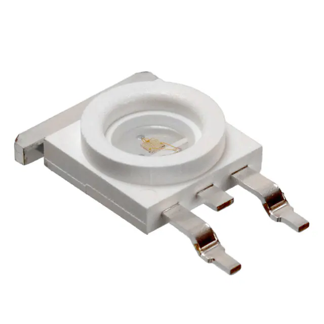


 工商网监
湘ICP备2023018690号
工商网监
湘ICP备2023018690号
