PI7C8952
PCI Dual UART
Datasheet
Revision 3
January 2019
1545 Barber Lane Milpitas, CA 95035
Telephone: 408-232-9100
FAX: 408-434-1040
Internet: http://www.diodes.com
Document Number DS40347 Rev 3-2
�PI7C8952
IMPORTANT NOTICE
DIODES INCORPORATED MAKES NO WARRANTY OF ANY KIND, EXPRESS OR IMPLIED, WITH REGARDS TO
THIS DOCUMENT, INCLUDING, BUT NOT LIMITED TO, THE IMPLIED WARRANTIES OF MERCHANTABILITY AND
FITNESS FOR A PARTICULAR PURPOSE (AND THEIR EQUIVALENTS UNDER THE LAWS OF ANY
JURISDICTION).
Diodes Incorporated and its subsidiaries reserve the right to make modifications, enhancements, improvements,
corrections or other changes without further notice to this document and any product described herein. Diodes
Incorporated does not assume any liability arising out of the application or use of this document or any product described
herein; neither does Diodes Incorporated convey any license under its patent or trademark rights, nor the rights of
others. Any Customer or user of this document or products described herein in such applications shall assume all risks
of such use and will agree to hold Diodes Incorporated and all the companies whose products are represented on Diodes
Incorporated website, harmless against all damages.
Diodes Incorporated does not warrant or accept any liability whatsoever in respect of any products purchased through
unauthorized sales channel.
Should Customers purchase or use Diodes Incorporated products for any unintended or unauthorized application,
Customers shall indemnify and hold Diodes Incorporated and its representatives harmless against all claims, damages,
expenses, and attorney fees arising out of, directly or indirectly, any claim of personal injury or death associated with
such unintended or unauthorized application.
Products described herein may be covered by one or more United States, international or foreign patents
pending. Product names and markings noted herein may also be covered by one or more United States, international or
foreign trademarks.
This document is written in English but may be translated into multiple languages for reference. Only the English version
of this document is the final and determinative format released by Diodes Incorporated.
LIFE SUPPORT
Diodes Incorporated products are specifically not authorized for use as critical components in life support devices or
systems without the express written approval of the Chief Executive Officer of Diodes Incorporated. As used herein:
A. Life support devices or systems are devices or systems which:
1. are intended to implant into the body, or
2. support or sustain life and whose failure to perform when properly used in accordance with instructions for
use provided in the labeling can be reasonably expected to result in significant injury to the user.
B. A critical component is any component in a life support device or system whose failure to perform can be reasonably
expected to cause the
failure of the life support device or to affect its safety or effectiveness.
Customers represent that they have all necessary expertise in the safety and regulatory ramifications of their life support
devices or systems, and acknowledge and agree that they are solely responsible for all legal, regulatory and safetyrelated requirements concerning their products and any use of Diodes Incorporated products in such safety-critical, life
support devices or systems, notwithstanding any devices- or systems-related information or support that may be provided
by Diodes Incorporated. Further, Customers must fully indemnify Diodes Incorporated and its representatives against
any damages arising out of the use of Diodes Incorporated products in such safety-critical, life support devices or
systems.
Copyright © 2016, Diodes Incorporated
www.diodes.com
PI7C8952
Document Number DS40347 Rev 3-2
Page 2 of 69
www.diodes.com
January 2019
© Diodes Incorporated
�PI7C8952
REVISION HISTORY
Date
09/12/14
12/09/15
Revision Number
0.1
1.0
01/06/16
1.1
09/09/16
1.2
09/20/17
01/31/19
2
3
PI7C8952
Document Number DS40347 Rev 3-2
Description
Preliminary Datasheet
Updated Section 1 Feature
Updated Section 6.3 Configuration Registers
Updated Section 9 Electrical Specification
Updated Section 9 Electrical Specification
Updated Section 11 Ordering Information
Updated Section 4 Pin Assignment
Updated Section 11 Ordering Information
Revision numbering system changed to whole number
Updated Section 1 Feature
Updated Section 7.2 Registers In I/O Mode
Updated Section 7.2.13 and 7.3.50 description
Added Part Marking
Page 3 of 69
www.diodes.com
January 2019
© Diodes Incorporated
�PI7C8952
Table of Contents
1.
FEATURES .......................................................................................................................................... 8
2.
APPLICATIONS ................................................................................................................................. 8
3.
GENERAL DESCRIPTION ............................................................................................................... 9
4.
PIN ASSIGNMENT ............................................................................................................................ 11
5.
FUNCTIONAL DESCRIPTION .......................................................................................................13
5.1. CONFIGURATION SPACE .........................................................................................................13
5.1.1.
PCI Configuration Space ......................................................................................................13
5.1.2.
UART Configuration Space ..................................................................................................13
5.2. DEVICE OPERATION .................................................................................................................14
5.2.1.
Configuration Access ............................................................................................................14
5.2.2.
I/O Reads/Writes ...................................................................................................................14
5.2.3.
Memory Reads/Writes ...........................................................................................................14
5.2.4.
Mode Selection......................................................................................................................14
5.2.5.
450/550 Mode .......................................................................................................................14
5.2.6.
Enhanced 550 Mode .............................................................................................................14
5.2.7.
Enhanced 950 Mode .............................................................................................................15
5.2.8.
Transmit and Receive FIFOs ................................................................................................15
5.2.9.
Automated Flow Control.......................................................................................................16
5.2.10. Internal Loopback .................................................................................................................17
5.2.11. Crystal Oscillator .................................................................................................................18
5.2.12. Baud Rate Generation ..........................................................................................................19
6.
PCI OPERATION ..............................................................................................................................20
6.1. SUPPORTED PCI TRANSACTION ............................................................................................20
6.2. REGISTER TYPES ......................................................................................................................20
6.3. CONFIGURATION REGISTERS ................................................................................................20
6.3.1.
VENDOR ID REGISTER – OFFSET 00h .............................................................................21
6.3.2.
DEVICE ID REGISTER – OFFSET 00h...............................................................................21
6.3.3.
COMMAND REGISTER – OFFSET 04h ..............................................................................21
6.3.4.
STATUS REGISTER – OFFSET 04h .....................................................................................21
6.3.5.
REVISION ID REGISTER – OFFSET 08h ...........................................................................22
6.3.6.
CLASS CODE REGISTER – OFFSET 08h ...........................................................................22
6.3.7.
CACHE LINE REGISTER – OFFSET 0Ch...........................................................................22
6.3.8.
MASTER LATENCY TIMER REGISTER – OFFSET 0Ch ....................................................22
6.3.9.
HEADER TYPE REGISTER – OFFSET 0Ch........................................................................22
6.3.10. BASE ADDRESS REGISTER 0 – OFFSET 10h ....................................................................23
6.3.11. BASE ADDRESS REGISTER 1 – OFFSET 14h ....................................................................23
6.3.12. SUBSYSTEM VENDOR REGISTER – OFFSET 2Ch ...........................................................23
6.3.13. SUBSYSTEM ID REGISTER – OFFSET 2Ch .......................................................................23
6.3.14. CAPABILITIES POINTER REGISTER – OFFSET 34h ........................................................23
6.3.15. INTERRUPT LINE REGISTER – OFFSET 3Ch ...................................................................23
6.3.16. INTERRUPT PIN REGISTER – OFFSET 3Ch .....................................................................23
6.3.17. EEPROM CONTROL REGISTER – OFFSET DCh ..............................................................24
7.
UART REGISTER DESCRIPTION .................................................................................................25
7.1. REGISTER TYPES ......................................................................................................................25
7.2. REGISTERS IN I/O MODE .........................................................................................................25
7.2.1.
RECEIVE HOLDING REGISTER – OFFSET 00h ...............................................................26
PI7C8952
Document Number DS40347 Rev 3-2
Page 4 of 69
www.diodes.com
January 2019
© Diodes Incorporated
�PI7C8952
7.2.2.
TRANSMIT HOLDING REGISTER – OFFSET 00h .............................................................26
7.2.3.
INTERRUPT ENABLE REGISTER – OFFSET 01h .............................................................27
7.2.4.
INTERRUPT STATUS REGISTER – OFFSET 02h ...............................................................27
7.2.5.
FIFO CONTROL REGISTER – OFFSET 02h ......................................................................27
7.2.6.
LINE CONTROL REGISTER – OFFSET 03h.......................................................................28
7.2.7.
MODEM CONTROL REGISTER – OFFSET 04h ................................................................29
7.2.8.
LINE STATUS REGISTER – OFFSET 05h ...........................................................................29
7.2.9.
MODEM STATUS REGISTER – OFFSET 06h .....................................................................30
7.2.10. SPECIAL FUNCTION REGISTER – OFFSET 07h ..............................................................31
7.2.11. DIVISOR LATCH LOW REGISTER – OFFSET 00h, LCR[7] = 1 .......................................31
7.2.12. DIVISOR LATCH HIGH REGISTER – OFFSET 01h, LCR[7] = 1......................................31
7.2.13. SAMPLE CLOCK REGISTER – OFFSET 02h, LCR[7] = 1 ................................................32
7.3. REGISTERS IN MEMORY-MAPPING MODE ..........................................................................33
7.3.1.
RECEIVE HOLDING REGISTER – OFFSET 00h ...............................................................38
7.3.2.
TRANSMIT HOLDING REGISTER – OFFSET 00h .............................................................38
7.3.3.
INTERRUPT ENABLE REGISTER – OFFSET 01h .............................................................39
7.3.4.
INTERRUPT STATUS REGISTER – OFFSET 02h ...............................................................39
7.3.5.
FIFO CONTROL REGISTER – OFFSET 02h ......................................................................39
7.3.6.
LINE CONTROL REGISTER – OFFSET 03h.......................................................................40
7.3.7.
MODEM CONTROL REGISTER – OFFSET 04h ................................................................41
7.3.8.
LINE STATUS REGISTER – OFFSET 05h ...........................................................................41
7.3.9.
MODEM STATUS REGISTER – OFFSET 06h .....................................................................42
7.3.10. SPECIAL FUNCTION REGISTER – OFFSET 07h ..............................................................43
7.3.11. DIVISOR LATCH LOW REGISTER – OFFSET 08h ............................................................43
7.3.12. DIVISOR LATCH HIGH REGISTER – OFFSET 09h...........................................................43
7.3.13. ENHANCED FUNCTION REGISTER – OFFSET 0Ah ........................................................44
7.3.14. XON SPECIAL CHARACTER 1 – OFFSET 0Bh ..................................................................45
7.3.15. XON SPECIAL CHARACTER 2 – OFFSET 0Ch..................................................................45
7.3.16. XOFF SPECIAL CHARACTER 1 – OFFSET 0Dh ...............................................................45
7.3.17. XOFF SPECIAL CHARACTER 2 – OFFSET 0Eh................................................................45
7.3.18. ADVANCE CONTROL REGISTER – OFFSET 0Fh .............................................................45
7.3.19. TRANSMIT INTERRUPT TRIGGER LEVEL – OFFSET 10h...............................................46
7.3.20. RECEIVE INTERRUPT TRIGGER LEVEL – OFFSET 11h .................................................46
7.3.21. FLOW CONTROL LOW TRIGGER LEVEL – OFFSET 12h ................................................46
7.3.22. FLOW CONTROL HIGH TRIGGER LEVEL – OFFSET 13h ..............................................46
7.3.23. CLOCK PRESCALE REGISTER – OFFSET 14h .................................................................47
7.3.24. RECEIVE FIFO DATA COUNTER – OFFSET 15h, SFR[6] = 0 .........................................47
7.3.25. LINE STATUS REGISTER COUNTER – OFFSET 15h, SFR[6] = 1 ...................................47
7.3.26. TRANSMIT FIFO DATA COUNTER – OFFSET 16h, SFR[7] = 1 ......................................47
7.3.27. SAMPLE CLOCK REGISTER – OFFSET 16h, SFR[7] = 0.................................................47
7.3.28. GLOBAL LINE STATUS REGISTER – OFFSET 17h ...........................................................48
7.3.29. GLOBAL INTERRUPT ENABLE REGISTER – OFFSET 18h..............................................48
7.3.30. GLOBAL INTERRUPT STATUS REGISTER – OFFSET 19h ...............................................48
7.3.31. TX OVERRUN REGISTER – OFFSET 1Ah ..........................................................................48
7.3.32. RX OVERRUN REGISTER – OFFSET 1Bh..........................................................................49
7.3.33. INTERRUPT STATUS REGISTER – OFFSET 1Ch ..............................................................49
7.3.34. RX FIFO COUNTER – OFFSET 1Dh ..................................................................................49
7.3.35. TX FIFO COUNTER – OFFSET 1Eh ...................................................................................49
7.3.36. FCR MIRROR REGISTER – OFFSET 1Fh ..........................................................................49
7.3.37. USER DEFINED TIMEOUT COUNTER REGISTER-1 – OFFSET 20h ..............................50
7.3.38. USER DEFINED TIMEOUT COUNTER REGISTER-2 – OFFSET 21h ..............................50
7.3.39. USER DEFINED TRIGGER LEVEL REGISTER – OFFSET 22h ........................................50
7.3.40. USER DEFINED REGISTER ENABLE – OFFSET 23h .......................................................50
7.3.41. TX IDLE COUNTER REGISTER– OFFSET 24h .................................................................50
PI7C8952
Document Number DS40347 Rev 3-2
Page 5 of 69
www.diodes.com
January 2019
© Diodes Incorporated
�PI7C8952
7.3.42.
7.3.43.
7.3.44.
7.3.45.
7.3.46.
7.3.47.
7.3.48.
7.3.49.
7.3.50.
7.3.51.
7.3.52.
7.3.53.
7.3.54.
7.3.55.
7.3.56.
7.3.57.
7.3.58.
7.3.59.
7.3.60.
7.3.61.
7.3.62.
7.3.63.
7.3.64.
7.3.65.
7.3.66.
7.3.67.
7.3.68.
7.3.69.
7.3.70.
8.
TX IDLE ENABLE REGISTER– OFFSET 25h .....................................................................50
SPECIAL CHARACTER 1 REGISTER– OFFSET 28h .........................................................50
SPECIAL CHARACTER 2 REGISTER– OFFSET 29h .........................................................51
SPECIAL CHARACTER 3 REGISTER– OFFSET 2Ah.........................................................51
SPECIAL CHARACTER 4 REGISTER– OFFSET 2Bh.........................................................51
SPECIAL CHARACTER ENABLE / CLEAR REGISTER– OFFSET 2Ch.............................51
FLASH LSR/TX_EMPTY INTERRUPT REGISTER– OFFSET 2Dh ....................................51
IN BAND TRANSMIT FLOW CONTROL REGISTER– OFFSET 2Eh .................................51
ADVANCE CONTROL REGISTER– OFFSET 2Fh ..............................................................51
RECEIVE FIFO DATA REGISTERS – OFFSET 100h ~ 17Fh .............................................52
TRANSMIT FIFO DATA REGISTERS – OFFSET 100h ~ 17Fh...........................................52
LINE STATUS FIFO REGISTERS –OFFSET 180h ~ 1FFh .................................................52
GLOBAL INTERRUPT REGISTERS 0 –OFFSET 40h .........................................................52
GLOBAL INTERRUPT REGISTERS 1 –OFFSET 41h .........................................................52
GLOBAL INTERRUPT REGISTERS 2 –OFFSET 42h .........................................................53
GLOBAL INTERRUPT REGISTERS 3 –OFFSET 43h .........................................................53
TIMER CONTROL REGISTER –OFFSET 44h ....................................................................53
TIMER/COUNTER LATCH LSB REGISTER –OFFSET 46h ...............................................54
TIMER/COUNTER LATCH MSB REGISTER –OFFSET 47h ..............................................54
SOFTWARE RESET REGISTER –OFFSET 4Ah ..................................................................54
SLEEP MODE CONTROL REGISTER –OFFSET 4Bh ........................................................54
DEVICE REVISION REGISTER –OFFSET 4Ch ..................................................................54
DEVICE IDENTIFICATION REGISTER –OFFSET 4Dh ....................................................54
SIMULTANEOUS CONFIGURATION ALL UART REGISTER –OFFSET 4Eh ...................55
GENERALPURPOSE IO INTERRUPT MASK REGISTER –OFFSET 4Fh .........................55
GENERALPURPOSE IO OUTPUT LEVEL CONTROL REGISTER –OFFSET 50h ...........55
GENERALPURPOSE IO OUTPUT STATE CONTROL REGISTER –OFFSET 51h ............55
GENERALPURPOSE IO INPUT POLARITY SELECT REGISTER –OFFSET 52h.............55
GENERALPURPOSE IO SELECT REGISTER –OFFSET 53h ............................................55
EEPROM INTERFACE.....................................................................................................................56
8.1.
8.2.
9.
EEPROM MODE AT RESET .......................................................................................................56
EEPROM SPACE ADDRESS MAP AND DESCRIPTION .........................................................56
ELECTRICAL SPECIFICATION ....................................................................................................57
10.
PACKAGE INFORMATION ........................................................................................................67
11.
ORDER INFORMATION .............................................................................................................69
PI7C8952
Document Number DS40347 Rev 3-2
Page 6 of 69
www.diodes.com
January 2019
© Diodes Incorporated
�PI7C8952
Table of Tables
TABLE 5-1 MODE SELECTION ........................................................................................................................14
TABLE 5-2 BAUD RATE GENERATOR SETTING ...............................................................................................19
TABLE 5-3 SAMPLE BAUD RATE SETTING ......................................................................................................19
TABLE 7-1 UART BASE ADDRESS IN I/O MODE ............................................................................................25
TABLE 7-2 REGISTERS IN I/O MODE ..............................................................................................................25
TABLE 7-3 UART BASE ADDRESS IN MEMORY MODE...................................................................................33
TABLE 7-4 MEMORY-MAP MODE ...................................................................................................................33
List of Figures
FIGURE 3-1 PI7C8952 BLOCK DIAGRAM ....................................................................................................... 9
FIGURE 3-2 PIN OUT ......................................................................................................................................10
FIGURE 5-1 TRANSMIT AND RECEIVE FIFOS .................................................................................................16
FIGURE 5-2 INTERNAL LOOPBACK IN PI7C8952 ............................................................................................17
FIGURE 5-3 CRYSTAL OSCILLATOR AS THE CLOCK SOURCE...........................................................................18
FIGURE 5-4 EXTERNAL CLOCK SOURCE AS THE CLOCK SOURCE ...................................................................18
FIGURE 7-1 UART REGISTER BLOCK ARRANGEMENT IN I/O MODE..............................................................25
FIGURE 7-2 UART REGISTER BLOCK ARRANGEMENT IN MEMORY MODE ...................................................33
FIGURE 9-1 TIMING FOR EXTERNAL CLOCK INPUT AT XTAL1 PIN ................................................................61
FIGURE 9-2 PCI BUS CONFIGURATION SPACE AND UART REGISTERS READ AND WRITE OPERATION...........62
FIGURE 9-3 RECEIVE DATA BURST READ OPERATION ....................................................................................63
FIGURE 9-4 TRANSMIT DATA BURST WRITE OPERATION ...............................................................................63
FIGURE 9-5 5V PCI BUS CLOCK (DC TO 66MHZ) .........................................................................................64
FIGURE 9-6 3.3V PCI BUS CLOCK (DC TO 66MHZ) ......................................................................................65
FIGURE 9-7 TRANSMIT DATA INTERRUPT AT TRIGGER LEVEL ........................................................................66
FIGURE 9-8 RECEIVE DATA READY INTERRUPT AT TRIGGER LEVEL ..............................................................66
FIGURE 10-1 PACKAGE OUTLINE DRAWING...................................................................................................67
FIGURE 10-2 PART MARKING.........................................................................................................................68
PI7C8952
Document Number DS40347 Rev 3-2
Page 7 of 69
www.diodes.com
January 2019
© Diodes Incorporated
�PI7C8952
1. FEATURES
•
•
•
•
•
•
•
•
•
•
•
•
•
•
•
•
•
•
•
•
•
•
•
•
•
•
•
•
Two high performance 950-class UARTs
Universal PCI Bus Buffers – Auto sense 3.3V or 5V operation
32-bit PCI Bus 2.3 target signaling compliance
Fully 16C550 software compatible UARTs
128-byte FIFO for each transmitter and receiver
Baud rate up to 15 Mbps in asynchronous mode
Flexible clock prescaler from 4 to 46
Data Transfer in Byte, Word and Double-word
Data Read/Write Burst Operation
Automated in-band flow control using programmable Xon/Xoff in both directions
Automated out-of-band flow control using CTS#/RTS# and/or DSR#/DTR#
Arbitrary trigger levels for receiver and transmitter FIFO interrupts and automatic in-band and outof-band flow control
Global Interrupt Status and readable FIFO levels to facilitate implementation of efficient device
drivers
Detection of bad data in the receiver FIFO
Data framing size including 5, 6, 7, 8 and 9 bits
Infrared (IrDA 1.0/1.1) Data Encoder/Decoder
Auto RS-485 Half-duplex Output with Control Polarity Selector
Eight General Purpose Inputs/Outputs
A General Purpose 16-bit Timer/Counter
Hardware reconfiguration through Microwire compatible EEPROM
Operations via I/O or memory mapping
Sleep Mode with Automatic Wake-up
Dual power operation (3.3V or 5.0V for PCI I/O and 1.8V-5.0V for UART I/O)
Power dissipation: 0.2W typical in normal mode
Industrial Temperature Range -40o to 85o
Totally Lead-Free & Fully RoHS Compliant (Notes 1 & 2)
Halogen and Antimony Free. “Green” Device (Note 3)
100-pin LQFP package
2. APPLICATIONS
•
•
•
•
•
•
•
•
•
•
•
Remote Access Servers
Network / Storage Management
Factory Automation and Process Control
Instrumentation
Multi-port RS-232/ RS-422/ RS-485 Cards
Point-of-Sale Systems (PoS)
Industrial PC (IPC)
Industrial Control
Gaming Machines
Building Automation
Embedded Systems
Notes:
1. No purposely added lead. Fully EU Directive 2002/95/EC (RoHS), 2011/65/EU (RoHS 2) & 2015/863/EU (RoHS 3) compliant.
2. See https://www.diodes.com/quality/lead-free/ for more information about Diodes Incorporated’s definitions of Halogen- and Antimony-free, "Green" and Lead-free.
3. Halogen- and Antimony-free "Green” products are defined as those which contain
很抱歉,暂时无法提供与“PI7C8952AFAE”相匹配的价格&库存,您可以联系我们找货
免费人工找货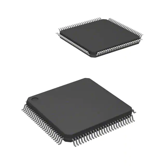


 工商网监
湘ICP备2023018690号
工商网监
湘ICP备2023018690号
