PL
IA
NT
CO
M
*R
oH
S
TISP4072F3LM THRU TISP4082F3LM,
TISP4125F3LM THRU TISP4180F3LM,
TISP4240F3LM THRU TISP4380F3LM
BIDIRECTIONAL THYRISTOR OVERVOLTAGE PROTECTORS
TISP4xxxF3LM Overvoltage Protector Series
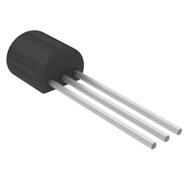
LM Package (Top View)
Ion-Implanted Breakdown Region
Precise and Stable Voltage
Low Voltage Overshoot under Surge
Device
‘4072
‘4082
‘4125
‘4150
‘4180
‘4240
‘4260
‘4290
‘4320
‘4380
VDRM
V(BO)
V
58
66
100
120
145
180
200
220
240
270
V
72
82
125
150
180
240
260
290
320
380
T(A)
NC
R(B)
1
2
3
MD4XAT
NC - No internal connection on pin 2
LMF Package (LM Package with Formed Leads) (Top View)
T(A)
E
T
E
L
O
S
B
O
NC
R(B)
Standard
10/160 μs
0.5/700 μs
10/700 μs
10/560 μs
10/1000 μs
FCC Part 68
I3124
ITU-T K.20/21
FCC Part 68
REA PE-60
MD4XAKB
NC - No internal connection on pin 2
Device Symbol
Rated for International Surge Wave Shapes
Waveshape
1
2
3
T
ITSP
A
60
38
50
45
35
R
SD4XAA
Terminals T and R correspond to the
alternative line designators of A and B
................................................UL Recognized Component
Description
These devices are designed to limit overvoltages on the telephone line. Overvoltages are normally caused by a.c. power system or lightning
flash disturbances which are induced or conducted on to the telephone line. A single device provides 2-point protection and is typically used
for the protection of 2-wire telecommunication equipment (e.g. between the Ring to Tip wires for telephones and modems). Combinations of
devices can be used for multi-point protection (e.g. 3-point protection between Ring, Tip and Ground).
The protector consists of a symmetrical voltage-triggered bidirectional thyristor. Overvoltages are initially clipped by breakdown clamping until the voltage rises to the breakover level, which causes the device to crowbar into a low-voltage on state. This low-voltage on state causes
the current resulting from the overvoltage to be safely diverted through the device. The high crowbar holding current helps prevent d.c. latchup
as the diverted current subsides.
How to Order
Device
TISP4xxxF3LM
Package
Carrier
Order As
Bulk Pack
TISP4xxxF3LM-S
Tape and Reeled
TISP4xxxF3LMR-S
Formed Lead DO-92 (LMF) Tape and Reeled
TISP4xxxF3LMFR-S
Straight Lead DO-92 (LM)
Insert xxx value corresponding to protection voltages of 072, 082, 125 etc.
NOVEMBER 1997 - REVISED JANUARY 2010
*RoHS Directive 2002/95/EC Jan 27 2003 including Annex.
Specifications are subject to change without notice.
Customers should verify actual device performance in their specific applications.
�TISP4xxxF3LM Overvoltage Protector Series
Description (Continued)
This TISP4xxxF3LM range consists of ten voltage variants to meet various maximum system voltage levels (58 V to 270 V). They are
guaranteed to voltage limit and withstand the listed international lightning surges in both polarities. These protection devices are supplied
in a DO-92 (LM) cylindrical plastic package. The TISP4xxxF3LM is a straight lead DO-92 supplied in bulk pack and on tape and reeled. The
TISP4xxxF3LMF is a formed lead DO-92 supplied only on tape and reeled.
Absolute Maximum Ratings, TA = 25 °C (Unless Otherwise Noted)
Rating
Symbol
‘4072
‘4082
‘4125
‘4150
‘4180
‘4240
‘4260
‘4290
‘4320
‘4380
E
T
E
L
O
S
B
O
Repetitive peak off-state voltage (0 °C < TJ < 70 °C)
Non-repetitive peak on-state pulse current (see Notes 1, 2 and 3)
2/10 µs (FCC Part 68, 2/10 µs voltage wave shape) excluding ‘4072 - ‘4082
8/20 µs (ANSI C62.41, 1.2/50 µs voltage wave shape) excluding ‘4072 - ‘4082
10/160 µs (FCC Part 68, 10/160 µs voltage wave shape)
5/200 µs (VDE 0433, 2 kV, 10/700 µs voltage wave shape)
0.2/310 µs (I3124, 1.5 kV, 0.5/700 µs voltage wave shape)
5/310 µs (ITU-T K.20/21, 1.5 kV, 10/700 µs voltage wave shape)
5/310 µs (FTZ R12, 2 kV, 10/700 µs voltage wave shape)
10/560 µs (FCC Part 68, 10/560 µs voltage wave shape)
10/1000 µs (REA PE-60, 10/1000 µs voltage wave shape)
2/10 µs (FCC Part 68, 2/10 µs voltage wave shape) ‘4072 - ‘4082 only
8/20 µs (ANSI C62.41, 1.2/50 µs voltage wave shape) ‘4072 - ‘4082 only
Non-repetitive peak on-state current (see Notes 2 and 3)
50/60 Hz, 1 s
Initial rate of rise of on-state current, Linear current ramp, Maximum ramp value < 38 A
Junction temperature
Storage temperature range
VDRM
ITSP
Value
± 58
± 66
± 100
± 120
± 145
± 180
± 200
± 220
± 240
± 270
175
120
60
50
38
38
50
45
35
80
70
Unit
V
A
ITSM
4
A
diT/dt
TJ
Tstg
250
-40 to +150
-55 to +150
A/µs
°C
°C
NOTES: 1. Initially the TISP must be in thermal equilibrium with 0 °C < TJ < 70 °C.
2. The surge may be repeated after the TISP returns to its initial conditions.
3. Above 70 °C, derate linearly to zero at 150 °C lead temperature.
NOVEMBER 1997 - REVISED JANUARY 2010
Specifications are subject to change without notice.
Customers should verify actual device performance in their specific applications.
�TISP4xxxF3LM Overvoltage Protector Series
Electrical Characteristics, TA = 25 °C (Unless Otherwise Noted)
IDRM
V(BO)
V(BO)
I(BO)
VT
IH
dv/dt
ID
Coff
Parameter
Repetitive peak offstate current
Breakover voltage
Test Conditions
Typ
VD = ±V DRM, 0 °C < TJ < 70 °C
E
T
E
L
O
S
B
O
dv/dt = ±1000
di/dt < 20 A/μs
Breakover current
On-state voltage
Holding current
Critical rate of rise of
off-state voltage
Off-state current
dv/dt = ±250 V/ms, RSOURCE = 300
IT = ±5 A,t W = 100 μs
IT = ±5 A,d i/dt = - /+ 30 mA/ms
RSOURCE = 50
Max
Unit
±10
A
±72
±82
±125
±150
±180
±240
±260
±290
±320
±380
±86
±96
±143
±168
±198
±267
±287
±317
±347
±407
±0.6
±3
‘4072
‘4082
‘4125
‘4150
‘4180
‘4240
‘4260
‘4290
‘4320
‘4380
‘4072
‘4082
‘4125
‘4150
‘4180
‘4240
‘4260
‘4290
‘4320
‘4380
dv/dt = ±250 V/ms, RSOURCE = 300
Impulse breakover
voltage
Off-state capacitance
Min
±0.15
±0.15
±5
Linear voltage ramp, Maximum ramp value < 0.85VDRM
VD = ±50 V
f = 100 kHz, Vd = 1 Vr .m.s.,V D = 0,
f = 100 kHz, Vd = 1 Vr .m.s.,V D = -50 V
‘4072 - ‘4082
‘4125 - ‘4180
‘4240 - ‘4380
‘4072 - ‘4082
‘4125 - ‘4180
‘4240 - ‘4380
V
V
A
V
A
kV
63
43
44
25
15
11
±10
108
74
74
40
25
20
Typ
Max
Unit
120
°C/W
A
pF
Thermal Characteristics
Parameter
RΘJA
Junction to free air thermal resistance
Test Conditions
EIA/JESD51-3 PCB mounted in an EIA/
JESD51-2 enclosure
NOVEMBER 1997 - REVISED JANUARY 2010
Specifications are subject to change without notice.
Customers should verify actual device performance in their specific applications.
Min
�TISP4xxxF3LM
TISP4xxxF3LMOvervoltage
OvervoltageProtector
ProtectorSeries
Series
Parameter Measurement Information
+i
Quadrant I
ITSP
Switching
Characteristic
ITSM
IT
V(BO)
VT
I(BO)
IH
E
T
E
L
O
S
B
O
IDRM
VDRM
-v
ID
VD
ID
VD
VDRM
+v
IDRM
IH
I(BO)
V(BO)
VT
IT
ITSM
Quadrant III
Switching
Characteristic
ITSP
-i
PMXXAAB
Figure 1. Voltage- Current Characteristic for R and T Terminals
All Measurements are Referenced to the T Terminal
NOVEMBER 1997 - REVISED JANUARY 2010
Specifications are subject to change without notice.
Customers should verify actual device performance in their specific applications.
�TISP4xxxF3LM
TISP4xxxF3LM Overvoltage
Overvoltage Protector
Protector Series
Series
Typical Characteristics
OFF-STATE CURRENT
vs
JUNCTION TEMPERATURE
100
VDRM DERATING FACTOR
vs
MINIMUM AMBIENT TEMPERATURE
TC4XAA
1.00
0.99
Derating Factor
ID - Off-State Current - µA
10
1
0.97
VD = -50 V
0.96
0·01
0·001
-25
0
25
50
75
100 125
TJ - Junction Temperature - °C
0.95
-40
150
'4240
THRU
'4380
-35
-30
-25
-20
-15
-10
-5
TAMIN - Minimum Ambient Temperature - °C
Figure 2.
V(BO)I Normalized
to 25 °Ct -Value
- On-State Curren
A
10 '4240
THRU
1.0
'4380
TC3MAL
TC4XAC
'4072
AND
'4082
T
'4240
THRU
'4380
25°C
'4072
150°C
AND
'4082
1 -25
NORMALIZED HOLDING CURRENT
vs
JUNCTION TEMPERATURE
2.0
TC4XAD
1.5
Normalized Holding Current
'4125
THRU
'4180
1.1
0
Figure 3.
NORMALIZED V(BO)
vs
AMBIENT TEMPERATURE
100
0.91
'4125
THRU
'4180
E
T
E
L
O
S
B
O
VD = 50 V
0·1
'4072
AND
'4082
0.98
TC4XAB
1.0
0.9
0.8
0.7
0.6
0.5
-40°C
0.4
225
13
5 6 125
7 8 9150
0
50
754
100
- On-State
Voltage - -V°C
TA -VAmbient
Temperature
T
Figure 4.
NOVEMBER 1997 - REVISED JANUARY 2010
Specifications are subject to change without notice.
Customers should verify actual device performance in their specific applications.
-25
0
25
50
75
100
TJ - Junction Temperature - °C
Figure 5.
125
150
�TISP4xxxF3LM Overvoltage Protector Series
Typical Characteristics
NORMALIZED BREAKOVER VOLTAGE
vs
RATE OF RISE OF PRINCIPLE CURRENT
TC4XAE
1.3
'4072
AND
'4082
Normalized Breakover Voltage
NEGATIVE POLARITY
1.2
'4240
THRU
'4380
1.1
TC4XAF
1.3
'4072
AND
'4082
POSITIVE POLARITY
Normalized Breakover Voltage
NORMALIZED BREAKOVER VOLTAGE
vs
RATE OF RISE OF PRINCIPLE CURRENT
'4125
THRU
'4180
1.2
E
T
E
L
O
S
B
O
'4240
THRU
'4380
1.1
'4125
THRU
'4180
1.0
0·001
0·01
0·1
1
10
1.0
0·001
100
di/dt - Rate of Rise of Principal Current - A/µs
0·01
0·1
1
10
di/dt - Rate of Rise of Principal Current - A/µs
Figure 6.
Figure 7.
OFF-STATE CAPACITANCE
vs
TERMINAL VOLTAGE
OFF-STATE CAPACITANCE
vs
TERMINAL VOLTAGE
TC4XAG
100
90
80
70
POSITIVE POLARITY
60
'4072
AND
'4082
50
Off-State Capacitance - pF
Off-State Capacitance - pF
100
90
80
70
40
30
'4125
THRU
'4180
20
10
0·1
1
10
Terminal Voltage - V
Figure 8.
100
NEGATIVE POLARITY
'4072
AND
'4082
60
50
40
30
20
'4240
THRU
'4380
50
TC4XAH
10
0·1
'4125
THRU
'4180
'4240
THRU
'4380
1
10
Terminal Voltage - V
50
Figure 9.
NOVEMBER 1997 - REVISED JANUARY 2010
Specifications are subject to change without notice.
Customers should verify actual device performance in their specific applications.
�TISP4xxxF3LM Overvoltage Protector Series
ITSM(t) - Non-Repetitive Peak On-State Current - A
Typical Characteristics
10
9
8
7
NON-REPETITIVE PEAK ON-STATE CURRENT
vs
CURRENT DURATION
TI4LAAA
VGEN = 600 Vrms, 50/60 Hz
RGEN(t) = 1.4*VGEN / ITSM(t)
6
5
4
E
T
E
L
O
S
B
O
3
2
1
0·1
1
10
100
t - Current Duration - s
Figure 10.
NOVEMBER 1997 - REVISED JANUARY 2010
Specifications are subject to change without notice.
Customers should verify actual device performance in their specific applications.
1000
�TISP4xxxF3LM Overvoltage Protector Series
MECHANICAL DATA
Device Symbolization Code
Devices will be coded as below.
Device
TISP4072F3
TISP4082F3
TISP4125F3
TISP4150F3
TISP4180F3
TISP4240F3
TISP4260F3
TISP4290F3
TISP4320F3
TISP4380F3
Carrier Information
Symbolization Code
4072F3
4082F3
4125F3
4150F3
4180F3
4240F3
4260F3
4290F3
4320F3
4380F3
E
T
E
L
O
S
B
O
Devices are shipped in one of the carriers below. A reel contains 2,000 devices.
Device
TISP4xxxF3LM
Package
Straight Lead DO-92 (LM)
Carrier
Order As
Bulk Pack
TISP4xxxF3LM-S
Tape and Reeled
TISP4xxxF3LMR-S
Formed Lead DO-92 (LMF) Tape and Reeled
TISP4xxxF3LMFR-S
Insert xxx value corresponding to protection voltages of 072, 082, 125 etc.
“TISP” is a trademark of Bourns, Ltd., a Bourns Company, and is Registered in U.S. Patent and Trademark Office.
“Bourns” is a registered trademark of Bourns, Inc. in the U.S. and other countries.
NOVEMBER 1997 - REVISED JANUARY 2010
Specifications are subject to change without notice.
Customers should verify actual device performance in their specific applications.
�


 工商网监
湘ICP备2023018690号
工商网监
湘ICP备2023018690号
