TISP4070M3BJ THRU TISP4115M3BJ,
TISP4125M3BJ THRU TISP4220M3BJ,
TISP4240M3BJ THRU TISP4400M3BJ
BIDIRECTIONAL THYRISTOR OVERVOLTAGE PROTECTORS
TISP4xxxM3BJ Overvoltage Protector Series
ITU-T K.20/21/44/45 rating
............................ 4 kV 10/700, 100 A 5/310
Ion-Implanted Breakdown Region
Precise and Stable Voltage
Low Voltage Overshoot under Surge
Device
‘4070
‘4080
‘4095
‘4115
‘4125
‘4145
‘4165
‘4180
‘4200
‘4220
‘4240
‘4250
‘4265
‘4290
‘4300
‘4350
‘4360
‘4395
‘4400
VDRM
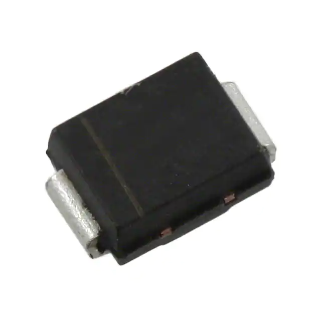
SMBJ Package (Top View)
Click these links for more information:
2 T(A)
R(B) 1
PRODUCT TECHNICAL INVENTORY SAMPLES
SELECTOR LIBRARY
V(BO)
V
V
58
65
75
90
100
120
135
145
155
160
180
190
200
220
230
275
290
320
300
70
80
95
115
125
145
165
180
200
220
240
250
265
290
300
350
360
395
400
Additional Information
Agency Recognition
Device Symbol
Description
T
UL
Package
File Number: E215609
Low Differential Capacitance.. 39 pF max.
............UL Recognized Component
SD4XAA
R
Description
T erminals T and R correspond to the
alternative line designators of A and B
Wave
Shape
Standard
ITSP
A
2/10 μs
GR-1089-CORE
300
8/20 μs
IEC 61000-4-5
220
10/160 μs
FCC Part 68
120
10/700 μs
ITU-T K.20/21/45
100
10/560 μs
FCC Part 68
75
10/1000 μs
GR-1089-CORE
50
How to Order
Device
CONTACT
MDXXBGE
Carrier
Order As
TISP4xxxM3BJ BJ (J-Bend DO-214AA/SMB) Embossed Tape Reeled TISP4xxxM3BJR-S
Insert xxx value corresponding to protection voltages of 070, 080, 095, 115, etc.
WARNING Cancer and Reproductive Harm
www.P65Warnings.ca.gov
NOVEMBER 1997 – REVISED JULY 2019
*RoHS Directive 2015/863, Mar 31, 2015 and Annex.
Specifications are subject to change without notice.
Users should verify actual device performance in their specific applications.
The products described herein and this document are subject to specific legal disclaimers as set forth on the last
page of this document, and at www.bourns.com/docs/legal/disclaimer.pdf.
These devices are designed to limit
overvoltages on the telephone line.
Overvoltages are normally caused by a.c.
power system or lightning flash disturbances
which are induced or conducted on to the
telephone line. A single device provides
2-point protection and is typically used for
the protection of 2-wire telecommunication
equipment (e.g. between the Ring and
Tip wires for telephones and modems).
Combinations of devices can be used for
multi-point protection (e.g. 3-point protection
between Ring, Tip and Ground).
The protector consists of a symmetrical
voltage-triggered bidirectional thyristor.
Overvoltages are initially clipped by
breakdown clamping until the voltage rises
to the breakover level, which causes the
device to crowbar into a low-voltage on
state. This low-voltage on state causes the
current resulting from the overvoltage to be
safely diverted through the device. The high
crowbar holding current helps prevent d.c.
latchup as the diverted current subsides.
The TISP4xxxM3BJ range consists of
nineteen voltage variants to meet various
maximum system voltage levels (58 V to
320 V). They are guaranteed to voltage
limit and withstand the listed international
lightning surges in both polarities. These
medium (M) current protection devices are
in a plastic package SMBJ (JEDEC DO214AA with J-bend leads) and supplied in
embossed tape reel pack. For alternative
voltage and holding current values, consult
the factory. For higher rated impulse
currents in the SMB package, the 100 A
10/1000 TISP4xxxH3BJ series is available.
�TISP4xxxM3BJ Overvoltage Protector Series
Absolute Maximum Ratings, TA = 25 °C (Unless Otherwise Noted)
Rating
Repetitive peak off-state voltage, (see Note 1)
Symbol
‘4070
‘4080
‘4095
‘4115
‘4125
‘4145
‘4165
‘4180
‘4200
‘4220
‘4240
‘4250
‘4265
‘4290
‘4300
‘4350
‘4360
‘4395
‘4400
VDRM
Value
±58
±65
±75
±90
±100
±120
±135
±145
±155
±160
±180
±190
±200
±220
±230
±275
±290
±320
±300
Unit
V
Non-repetitive peak on-state pulse current (see Notes 2, 3 and 4)
2/10 μs (GR-1089-CORE, 2/10 μs voltage wave shape)
300
8/20 μs (IEC 61000-4-5,combination wave generator, 1.2/50 voltage, 8/20 current)
220
10/160 μs (FCC Part 68, 10/160 μs voltage wave shape)
120
5/200 μs (VDE 0433, 10/700 μs voltage wave shape)
110
ITSP
A
0.2/310 μs (I3124, 0.5/700 μs voltage wave shape)
100
5/310 μ (ITU-T K.20/21/45, K.44 10/700 μs voltage wave shape)
100
5/310 μs (FTZ R12, 10/700 μs voltage wave shape)
100
10/560 μs (FCC Part 68, 10/560 μs voltage wave shape)
75
10/1000 μs (GR-1089-CORE, 10/1000 μs voltage wave shape)
50
Non-repetitive peak on-state current (see Notes 2, 3 and 5)
20 ms (50 Hz) full sine wave
30
ITSM
16.7 ms (60 Hz) full sine wave
32
A
1000 s 50 Hz/60 Hz a.c.
2.1
300
A/μs
Initial rate of rise of on-state current, Exponential current ramp, Maximum ramp value < 100 A
di T/dt
-40 to +150
°C
Junction temperature
TJ
-65 to +150
°C
Storage temperature range
Tstg
NOTES: 1. See Applications Information and Figure 11 for voltage values at lower temperatures.
2. Initially,the TISP4xxxM3BJ must be in thermal equilibrium with TJ = 25 °C.
3. The surge may be repeated after the TISP4xxxM3BJ returns to its initial conditions.
4. See Applications Information and Figure 12 for current ratings at other temperatures.
5. EIA/JESD51-2 environment and EIA/JESD51-3 PCB with standard footprint dimensions connected with 5 A rated printed wiring
track widths. See Figure 9 for the current ratings at other durations. Derate current values at -0.61 %/°C for ambient temperatures
above 25 °C.
NOVEMBER 1997 – REVISED JULY 2019
Specifications are subject to change without notice.
Users should verify actual device performance in their specific applications.
The products described herein and this document are subject to specific legal disclaimers as set forth on the last page of this document, and at www.bourns.com/docs/legal/disclaimer.pdf.
�TISP4xxxM3BJ Overvoltage Protector Series
Electrical Characteristics, TA = 25 °C (Unless Otherwise Noted)
IDRM
V(BO)
V(BO)
I(BO)
VT
IH
dv/dt
ID
Parameter
Repetitive peak offstate current
Breakover voltage
Impulse breakover
voltage
Breakover current
On-state voltage
Holding current
Critical rate of rise of
off-state voltage
Off-state current
Test Conditions
VD = VDRM
dv/dt = ±250 V/ms, R SOURCE = 300 Ω
dv/dt ≤ ±1000 V/μs, Linear voltage ramp,
Maximum ramp value = ±500 V
di/dt = ±20 A/μs, Linear current ramp,
Maximum ramp value = ±10 A
Min
TA = 25 °C
TA = 85 °C
‘4070
‘4080
‘4095
‘4115
‘4125
‘4145
‘4165
‘4180
‘4200
‘4220
‘4240
‘4250
‘4265
‘4290
‘4300
‘4350
‘4360
‘4395
‘4400
‘4070
‘4080
‘4095
‘4115
‘4125
‘4145
‘4165
‘4180
‘4200
‘4220
‘4240
‘4250
‘4265
‘4290
‘4300
‘4350
‘4360
‘4395
‘4400
dv/dt = ±250 V/ms, R SOURCE = 300 Ω
I T = ±5 A, t W = 100 μs
I T = ±5 A, di/dt = +/-30 mA/ms
±0.15
±0.15
Linear voltage ramp, Maximum ramp value < 0.85V DRM
VD = ±50 V
Typ
Max
±5
±10
±70
±80
±95
±115
±125
±145
±165
±180
±200
±220
±240
±250
±265
±290
±300
±350
±360
±395
±400
±78
±88
±102
±122
±132
±151
±171
±186
±207
±227
±247
±257
±272
±298
±308
±359
±370
±405
±410
±0.6
±3
±0.35
μA
V
V
A
V
A
kV/μs
±5
TA = 85 °C
Unit
±10
μA
NOVEMBER 1997 – REVISED JULY 2019
Specifications are subject to change without notice.
Users should verify actual device performance in their specific applications.
The products described herein and this document are subject to specific legal disclaimers as set forth on the last page of this document, and at www.bourns.com/docs/legal/disclaimer.pdf.
�TISP4xxxM3BJ Overvoltage Protector Series
Electrical Characteristics, TA = 25 °C (Unless Otherwise Noted)
Parameter
Test Conditions
f = 1 MHz , Vd = 1 V rms, VD = 0,
f = 1 MHz , Vd = 1 V rms, VD = -1 V
Coff
Off-state capacitance
f = 1 MHz , Vd = 1 V rms, VD = -2 V
f = 1 MHz , Vd = 1 V rms, VD = -50 V
f = 1 MHz , Vd = 1 V rms, VD = -100 V
(see Note 6)
NOTE
Min
4070 thru ‘4115
‘4125 thru ‘4220
‘4240 thru ‘4400
‘4070 thru ‘4115
‘4125 thru ‘4220
‘4240 thru ‘4400
‘4070 thru ‘4115
‘4125 thru ‘4220
‘4240 thru ‘4400
‘4070 thru ‘4115
‘4125 thru ‘4220
‘4240 thru ‘4400
‘4125 thru ‘4220
‘4240 thru ‘4400
Typ
83
62
50
78
56
45
72
52
42
36
26
19
21
15
Max
100
74
60
94
67
54
87
62
50
44
31
22
25
18
Unit
Typ
Max
Unit
pF
6: To avoid possible voltage clipping, the ‘4125 is tested with V D = -98 V.
Thermal Characteristics
Parameter
RθJA
NOTE
Junction to free air thermal resistance
Test Conditions
Min
EIA/JESD51-3 PCB, IT = ITSM(1000),
TA = 25 °C, (see Note 7)
265 mm x 210 mm populated line card,
4-layer PCB, IT = ITSM(1000), TA = 25 °C
115
°C/W
52
7: EIA/JESD51-2 environment and PCB has standard footprint dimensions connected with 5 A rated printed wiring track widths.
NOVEMBER 1997 – REVISED JULY 2019
Specifications are subject to change without notice.
Users should verify actual device performance in their specific applications.
The products described herein and this document are subject to specific legal disclaimers as set forth on the last page of this document, and at www.bourns.com/docs/legal/disclaimer.pdf.
�TISP4xxxM3BJ Overvoltage Protector Series
Parameter Measurement Information
+i
Quadrant I
ITSP
Switching
Characteristic
ITSM
IT
V(BO)
VT
I(BO)
IH
V DRM
-v
IDRM
ID
VD
ID
IDRM
VD
VDRM
+v
IH
I(BO)
VT
V(BO)
IT
ITSM
I
Quadrant III
ITSP
Switching
Characteristic
-i
PMXXAAB
Figure 1. Voltage-Current Characteristic for T and R Terminals
All Measurements are Referenced to the R Terminal
NOVEMBER 1997 – REVISED JULY 2019
Specifications are subject to change without notice.
Users should verify actual device performance in their specific applications.
The products described herein and this document are subject to specific legal disclaimers as set forth on the last page of this document, and at www.bourns.com/docs/legal/disclaimer.pdf.
�TISP4xxxM3BJ Overvoltage Protector Series
Typical Characteristics
OFF-STATE CURRENT
vs
JUNCTION TEMPERATURE
TCMAG
100
1.10
NORMALIZED BREAKOVER VOLTAGE
vs
JUNCTION TEMPERATURE TC4MAF
VD = ±50 V
Normalized Breakover Voltage
|ID| - Off-State Current - A
10
1
0·1
0·01
0·001
1.05
1.00
0.95
-25
0
25
50
75
100
TJ - Junction Temperature - °C
125
150
-25
100
50
40
30
TA = 25 °C
t W = 100 μs
10
5
4
3
2
1.5
1
0.7
'4125
THRU
'4200
'4240
THRU
'4400
1
NORMALIZED HOLDING CURRENT
vs
JUNCTION TEMPERATURE TC4MAD
1.5
20
15
7
2.0
TC4MACA
Normalized Hol ding Current
IT - On-State Current - A
70
150
Figure 3.
Figure 2.
ON-STATE CURRENT
vs
ON-STATE VOLTAGE
0
25
50
75
100 125
TJ - Junction Temperature - °C
Figure 4.
0.9
0.8
0.7
0.6
0.5
'4070
THRU
'4115
1.5
2
31 4 5
VT - On-State Voltage - V
1.0
0.4
7
10
-25
0
25
50
75
100
TJ - Junction Temperature - °C
125
150
Figure 5.
NOVEMBER 1997 – REVISED JULY 2019
Specifications are subject to change without notice.
Users should verify actual device performance in their specific applications.
The products described herein and this document are subject to specific legal disclaimers as set forth on the last page of this document, and at www.bourns.com/docs/legal/disclaimer.pdf.
�TISP4xxxM3BJ Overvoltage Protector Series
Typical Characteristics
TJ = 25 °C
Vd = 1 Vrms
Capacitance Normali zed to VD = 0
0.8
0.7
0.6
0.5
'4070 THRU '4115
0.4
'4125 THRU '4220
0.3
'4240 THRU '4400
0.2
0.5
TCMAEB
40
0.9
ΔC - Differential Off-State Capacitance- pF
1
DIFFERENTIAL OFF-STATE CAPACITANCE
vs
RATED REPETITIVE PEAK OFF-STATE VOLTAGE
NORMALIZED CAPACITANCE
vs
OFF-STATE VOLTAGE
TC4MABB
1
2
3
5
10
20 30
VD - Off-state Voltage - V
50
35
ΔC = Coff(-2 V) - Coff (-50 V)
30
25
20
100 150
50
Figure 6.
60 70 80 90 100
150
200 250 300 350
VDRM - Repetitive Peak Off-State Voltage - V
Figure 7.
|Coff(+VD) - Coff(-VD) | — Capacitance Asymmetry — pF
3
TYPICAL CAPACITANCE ASYMMETRY
vs
OFF-STATE VOLTAGE
TC4XBB
Vd = 10 mV rms, 1 MHz
2
1
Vd = 1 V rms, 1 MHz
0
0.5 0.7 1
2
3 4 5
7 10
20 30 4050
VD — Off-State Voltage — V
Figure 8.
NOVEMBER 1997 – REVISED JULY 2019
Specifications are subject to change without notice.
Users should verify actual device performance in their specific applications.
The products described herein and this document are subject to specific legal disclaimers as set forth on the last page of this document, and at www.bourns.com/docs/legal/disclaimer.pdf.
�TISP4xxxM3BJ Overvoltage Protector Series
Rating and Thermal Information
THERMAL IMPEDANCE
vs
POWER DURATION
TI4MAC
30
VGEN = 600 Vrms, 50/60 Hz
RGEN = 1.4*VGEN /ITSM(t)
EIA/JESD51-2 ENVIRONMENT
EIA/JESD51-3 PCB
TA = 25 °C
20
15
10
9
8
7
6
5
4
3
2
1.5
0·1
1
10
100
150
Z θA(t) - Transie nt Thermal Impedance - °C/W
ITSM(t) - Non-Repetitive Peak On-State Current - A
NON-REPETITIVE PEAK ON-STATE CURRENT
vs
CURRENT DURATION
1000
100
90
80
70
60
50
40
30
20
15
10
9
8
7
6
5
4
0·1
VDRM DERATING FACTOR
vs
MINIMUM AMBIENT TEMPERATURE
TI4MADA
400
100
1000
TC4MAA
BELLCORE 2/10
300
250
'4125 THRU '4200
Impulse Current - A
Derating Factor
10
IMPULSE RATING
vs
AMBIENT TEMPERATURE
0.99
0.97
0.96
0.95
1
Figure 10.
Figure 9.
0.98
ITSM(t) APPLIED FOR TIME t
EIA/JESD51-2 ENVIRONMENT
EIA/JESD51-3 PCB
TA = 25 °C
t - Power Duration - s
t - Current Duration - s
1.00
TI4MAE
'4070 THRU '4115
IEC 1.2/50, 8/20
200
150
FCC 10/160
120
100
90
80
70
ITU-T 10/700
FCC 10/560
60
0.94
50
'4240 THRU '4400
0.93
-40 -35 -30 -25 -20 -15 -10 -5
0
5
10 15 20 25
TAMIN - Minimum Ambient Temperature - °C
Figure 11.
40
-40 -30 -20 -10 0
BELLCORE 10/1000
10 20 30 40 50 60 70 80
TA - Ambient Temperature - °C
Figure 12.
NOVEMBER 1997 – REVISED JULY 2019
Specifications are subject to change without notice.
Users should verify actual device performance in their specific applications.
The products described herein and this document are subject to specific legal disclaimers as set forth on the last page of this document, and at www.bourns.com/docs/legal/disclaimer.pdf.
�TISP4xxxM3BJ Overvoltage Protector Series
APPLICATIONS INFORMATION
Deployment
These devices are two terminal overvoltage protectors. They may be used either singly to limit the voltage between two conductors
(Figure 13) or in multiples to limit the voltage at several points in a circuit (Figure 14).
Th3
Th1
Th1
Th2
Figure 14. Multi-Point Protection
Figure 13. Two Point Protection
In Figure 13, protector Th1 limits the maximum voltage between the two conductors to ±V(BO). This configuration is normally used to protect
circuits without a ground reference, such as modems. In Figure 14, protectors Th2 and Th3 limit the maximum voltage between each conductor
and ground to the ±V(BO) of the individual protector. Protector Th1 limits the maximum voltage between the two conductors to its ±V(BO)
value. If the equipment being protected has all its vulnerable components connected between the conductors and ground, then protector Th1 is
not required.
Impulse Testing
To verify the withstand capability and safety of the equipment, standards require that the equipment is tested with various impulse wave forms.
The table below shows some common values.
Standard
Peak Voltage
Setting
V
Voltage
Wave Shape
Peak Current
Value
A
Current
Wave Shape
TISP4XXXM3
25 °C Rating
A
Series
Resistance
2500
2/10
500
2/10
300
11
1000
10/1000
100
10/1000
50
1500
10/160
200
10/160
120
2x5.6
800
10/560
100
10/560
75
3
FCC Part 68
1500
9/720 †
37.5
5/320 †
100
0
(March 1998)
1000
9/720 †
25
5/320 †
100
0
I3124
1500
0.5/700
37.5
0.2/310
100
0
1500
37.5
ITU-T K.20/K.21
10/700
5/310
100
0
4000
100
† FCC Part 68 terminology for the waveforms produced by the ITU-T recommendation K.21 10/700 impulse generator
GR-1089-CORE
If the impulse generator current exceeds the protector’s current rating, then a series resistance can be used to reduce the current to the
protector’s rated value to prevent possible failure. The required value of series resistance for a given waveform is given by the following
calculations. First, the minimum total circuit impedance is found by dividing the impulse generator’s peak voltage by the protector’s rated
current. The impulse generator’s fictive impedance (generator’s peak voltage divided by peak short circuit current) is then subtracted from the
minimum total circuit impedance to give the required value of series resistance.
For the FCC Part 68 10/560 waveform, the following values result. The minimum total circuit impedance is 800/75 = 10.7 Ω and the generator’s
fictive impedance is 800/100 = 8 Ω. This gives a minimum series resistance value of 10.7 - 8 = 2.7 Ω. After allowing for tolerance, a 3 Ω ±10%
resistor would be suitable. The 10/160 waveform needs a standard resistor value of 5.6 Ω per conductor. These would be R1a and R1b in
Figure 16 and Figure 17. FCC Part 68 allows the equipment to be non-operational after the 10/160 (conductor to ground) and 10/560 (interconductor) impulses. The series resistor value may be reduced to zero to pass FCC Part 68 in a non-operational mode, e.g. Figure 15. For
this type of design, the series fuse must open before the TISP4xxxM3 fails. For Figure 15, the maximum fuse i2t is 2.3 A2s. In some cases, the
equipment will require verification over a temperature range. By using the rated waveform values from Figure 12, the appropriate series resistor
value can be calculated for ambient temperatures in the range of -40 °C to 85 °C.
NOVEMBER 1997 – REVISED JULY 2019
Specifications are subject to change without notice.
Users should verify actual device performance in their specific applications.
The products described herein and this document are subject to specific legal disclaimers as set forth on the last page of this document, and at www.bourns.com/docs/legal/disclaimer.pdf.
�TISP4xxxM3BJ Overvoltage Protector Series
AC Power Testing
The protector can withstand currents applied for times not exceeding those shown in Figure 9. Currents that exceed these times must be
terminated or reduced to avoid protector failure. Fuses, PTC (Positive Temperature Coefficient) thermistors and fusible resistors are overcurrent
protection devices which can be used to reduce the current flow. Protective fuses may range from a few hundred milliamperes to one ampere.
In some cases, it may be necessary to add some extra series resistance to prevent the fuse opening during impulse testing. The current versus
time characteristic of the overcurrent protector must be below the line shown in Figure 9. In some cases, there may be a further time limit
imposed by the test standard (e.g. UL 1459 wiring simulator failure).
Capacitance
The protector characteristic off-state capacitance values are given for d.c. bias voltage, VD, values of 0, -1 V, -2 V and -50 V. Where possible
values are also given for -100 V. Values for other voltages may be calculated by multiplying the VD = 0 capacitance value by the factor given in
Figure 6. Up to 10 MHz, the capacitance is essentially independent of frequency. Above 10 MHz, the effective capacitance is strongly dependent
on connection inductance. In many applications, such as Figure 16 and Figure 18, the typical conductor bias voltages will be about -2 V and -50
V. Figure 7 shows the differential (line unbalance) capacitance caused by biasing one protector at -2 V and the other at -50 V.
Figure 8 shows the typical capacitance asymmetry; the difference between the capacitance measured with a positive value of VD and the
capacitance value when the polarity of VD is reversed. Capacitance asymmetry is an important parameter in ADSL systems where the
protector often has no d.c. bias and the signal level is in the region of ±10 V.
Normal System Voltage Levels
The protector should not clip or limit the voltages that occur in normal system operation. For unusual conditions, such as ringing without the line
connected, some degree of clipping is permissible. Under this condition, about 10 V of clipping is normally possible without activating the ring
trip circuit.
Figure 11 allows the calculation of the protector VDRM value at temperatures below 25 °C. The calculated value should not be less than the
maximum normal system voltages. The TISP4265M3BJ, with a VDRM of 200 V, can be used for the protection of ring generators producing
100 V rms of ring on a battery voltage of -58 V (Th2 and Th3 in Figure 18). The peak ring voltage will be 58 + 1.414*100 = 199.4 V. However,
this is the open circuit voltage and the connection of the line and its equipment will reduce the peak voltage. In the extreme case of an
unconnected line, clipping the peak voltage to 190 V should not activate the ring trip. This level of clipping would occur at the temperature when
the VDRM has reduced to 190/200 = 0.95 of its 25 °C value. Figure 11 shows that this condition will occur at an ambient temperature of -28 °C.
In this example, the TISP4265M3BJ will allow normal equipment operation provided that the minimum expected ambient temperature does not
fall below -28 °C.
JESD51 Thermal Measurement Method
To standardize thermal measurements, the EIA (Electronic Industries Alliance) has created the JESD51 standard. Part 2 of the standard
(JESD51-2, 1995) describes the test environment. This is a 0.0283 m3 (1 ft3) cube which contains the test PCB (Printed Circuit Board)
horizontally mounted at the center. Part 3 of the standard (JESD51-3, 1996) defines two test PCBs for surface mount components; one for
packages smaller than 27 mm on a side and the other for packages up to 48 mm. The SMBJ measurements used the smaller 76.2 mm x
114.3 mm (3.0 “ x 4.5 “) PCB. The JESD51-3 PCBs are designed to have low effective thermal conductivity (high thermal resistance) and
represent a worst case condition. The PCBs used in the majority of applications will achieve lower values of thermal resistance, and can
dissipate higher power levels than indicated by the JESD51 values.
NOVEMBER 1997 – REVISED JULY 2019
Specifications are subject to change without notice.
Users should verify actual device performance in their specific applications.
The products described herein and this document are subject to specific legal disclaimers as set forth on the last page of this document, and at www.bourns.com/docs/legal/disclaimer.pdf.
�TISP4xxxM3BJ Overvoltage Protector Series
Typical Circuits
MODEM
TIP
WIRE
RING
FUSE
RING DETECTOR
R1a
Th3
HOOK SWITCH
Th1
D.C. SINK
TISP4350
PROTECTED
EQUIPMENT
Th2
SIGNAL
RING
WIRE
TIP
AI6XBMA
Figure 15. Modem Inter-Wire Protection
E.G. LINE CARD
R1b
AI6XBK
Figure 16. PROTECTION MODULE
R1a
Th3
SIGNAL
Th1
Th2
R1b
AI6XBL
D.C.
Figure 17. ISDN Protection
TIP
WIRE
OVERCURRENT
PROTECTION
RING/TEST
PROTECTION
TEST
RELAY
RING
RELAY
SLIC
RELAY
S3a
R1a
Th3
SLIC
PROTECTION
Th4
S2a
S1a
SLIC
Th1
Th2
RING
WIRE
Th5
R1b
S3b
S1b
S2b
TISP6xxxx,
TISPPBLx,
TISP6NTP2
C1
220 nF
TEST
EQUIPMENT
RING
GENERATOR
V BAT
AI6XBJ
Figure 18. Line Card Ring/Test Protection
NOVEMBER 1997 – REVISED JULY 2019
Specifications are subject to change without notice.
Users should verify actual device performance in their specific applications.
The products described herein and this document are subject to specific legal disclaimers as set forth on the last page of this document, and at www.bourns.com/docs/legal/disclaimer.pdf.
�TISP4xxxM3BJ Overvoltage Protector Series
Device Symbolization Code
Devices will be coded as below. As the device parameters are symmetrical, terminal 1 is not identified.
Device
TISP4070M3BJ
TISP4080M3BJ
TISP4095M3BJ
TISP4115M3BJ
TISP4125M3BJ
TISP4145M3BJ
TISP4165M3BJ
TISP4180M3BJ
TISP4200M3BJ
TISP4220M3BJ
TISP4240M3BJ
TISP4250M3BJ
TISP4265M3BJ
TISP4290M3BJ
TISP4300M3BJ
TISP4350M3BJ
TISP4360M3BJ
TISP4395M3BJ
TISP4400M3BJ
Symbolization
Code
4070M3
4080M3
4095M3
4115M3
4125M3
4145M3
4165M3
4180M3
4200M3
4220M3
4240M3
4250M3
4265M3
4290M3
4300M3
4350M3
4360M3
4395M3
4400M3
Asia-Pacific: Tel: +886-2 2562-4117 • Email: asiacus@bourns.com
EMEA: Tel: +36 88 885 877 • Email: eurocus@bourns.com
The Americas: Tel: +1-951 781-5500 • Email: americus@bourns.com
www.bourns.com
“TISP” is a trademark of Bourns, Ltd., a Bourns Company, and is Registered in the U.S. Patent and Trademark Office.
“Bourns” is a registered trademark of Bourns, Inc. in the U.S. and other countries.
NOVEMBER 1997 – REVISED JULY 2019
Specifications are subject to change without notice.
Users should verify actual device performance in their specific applications.
The products described herein and this document are subject to specific legal disclaimers as set forth on the last page of this document, and at www.bourns.com/docs/legal/disclaimer.pdf.
�
Legal Disclaimer Notice
This legal disclaimer applies to purchasers and users of Bourns® products manufactured by or on behalf of Bourns, Inc. and its
affiliates (collectively, “Bourns”).
Unless otherwise expressly indicated in writing, Bourns® products and data sheets relating thereto are subject to change
without notice. Users should check for and obtain the latest relevant information and verify that such information is current and
complete before placing orders for Bourns® products.
The characteristics and parameters of a Bourns® product set forth in its data sheet are based on laboratory conditions, and
statements regarding the suitability of products for certain types of applications are based on Bourns’ knowledge of typical
requirements in generic applications. The characteristics and parameters of a Bourns® product in a user application may vary
from the data sheet characteristics and parameters due to (i) the combination of the Bourns® product with other components
in the user’s application, or (ii) the environment of the user application itself. The characteristics and parameters of a Bourns®
product also can and do vary in different applications and actual performance may vary over time. Users should always verify
the actual performance of the Bourns® product in their specific devices and applications, and make their own independent
judgments regarding the amount of additional test margin to design into their device or application to compensate for
differences between laboratory and real world conditions.
Unless Bourns has explicitly designated an individual Bourns® product as meeting the requirements of a particular industry
standard (e.g., ISO/TS 16949) or a particular qualification (e.g., UL listed or recognized), Bourns is not responsible for any
failure of an individual Bourns® product to meet the requirements of such industry standard or particular qualification. Users of
Bourns® products are responsible for ensuring compliance with safety-related requirements and standards applicable to their
devices or applications.
Bourns® products are not recommended, authorized or intended for use in nuclear, lifesaving, life-critical or life-sustaining applications, nor in any other applications where failure or malfunction may result in personal injury, death, or severe property or
environmental damage. Unless expressly and specifically approved in writing by two authorized Bourns representatives on a
case-by-case basis, use of any Bourns® products in such unauthorized applications might not be safe and thus is at the user’s
sole risk. Life-critical applications include devices identified by the U.S. Food and Drug Administration as Class III devices and
generally equivalent classifications outside of the United States.
Bourns expressly identifies those Bourns® standard products that are suitable for use in automotive applications on such
products’ data sheets in the section entitled “Applications.” Unless expressly and specifically approved in writing by two
authorized Bourns representatives on a case-by-case basis, use of any other Bourns® standard products in an automotive
application might not be safe and thus is not recommended, authorized or intended and is at the user’s sole risk. If Bourns
expressly identifies a sub-category of automotive application in the data sheet for its standard products (such as infotainment
or lighting), such identification means that Bourns has reviewed its standard product and has determined that if such Bourns®
standard product is considered for potential use in automotive applications, it should only be used in such sub-category of
automotive applications. Any reference to Bourns® standard product in the data sheet as compliant with the AEC-Q standard
or “automotive grade” does not by itself mean that Bourns has approved such product for use in an automotive application.
Bourns® standard products are not tested to comply with United States Federal Aviation Administration standards generally
or any other generally equivalent governmental organization standard applicable to products designed or manufactured for
use in aircraft or space applications. Bourns expressly identifies Bourns® standard products that are suitable for use in aircraft
or space applications on such products’ data sheets in the section entitled “Applications.” Unless expressly and specifically
approved in writing by two authorized Bourns representatives on a case-by-case basis, use of any other Bourns® standard
product in an aircraft or space application might not be safe and thus is not recommended, authorized or intended and is at the
user’s sole risk.
The use and level of testing applicable to Bourns® custom products shall be negotiated on a case-by-case basis by Bourns and
the user for which such Bourns® custom products are specially designed. Absent a written agreement between Bourns and the
user regarding the use and level of such testing, the above provisions applicable to Bourns® standard products shall also apply
to such Bourns® custom products.
Users shall not sell, transfer, export or re-export any Bourns® products or technology for use in activities which involve the
design, development, production, use or stockpiling of nuclear, chemical or biological weapons or missiles, nor shall they use
Bourns® products or technology in any facility which engages in activities relating to such devices. The foregoing restrictions
apply to all uses and applications that violate national or international prohibitions, including embargos or international
regulations. Further, Bourns® products and Bourns technology and technical data may not under any circumstance be
exported or re-exported to countries subject to international sanctions or embargoes. Bourns® products may not, without prior
authorization from Bourns and/or the U.S. Government, be resold, transferred, or re-exported to any party not eligible
to receive U.S. commodities, software, and technical data.
To the maximum extent permitted by applicable law, Bourns disclaims (i) any and all liability for special, punitive, consequential,
incidental or indirect damages or lost revenues or lost profits, and (ii) any and all implied warranties, including implied warranties
of fitness for particular purpose, non-infringement and merchantability.
For your convenience, copies of this Legal Disclaimer Notice with German, Spanish, Japanese, Traditional Chinese and Simplified Chinese
bilingual versions are available at:
Web Page: http://www.bourns.com/legal/disclaimers-terms-and-policies
PDF: http://www.bourns.com/docs/Legal/disclaimer.pdf
C1753 05/17/18R
�


 工商网监
湘ICP备2023018690号
工商网监
湘ICP备2023018690号
