ADC10D040
www.ti.com
SNAS149G – OCT 2001 – REVISED MARCH 2013
ADC10D040 Dual 10-Bit, 40 MSPS, 267 mW A/D Converter
Check for Samples: ADC10D040
FEATURES
DESCRIPTION
•
•
•
•
•
The ADC10D040 is a dual low power, high
performance CMOS analog-to-digital converter that
digitizes signals to 10 bits resolution at sampling
rates up to 45 MSPS while consuming a typical 267
mW from a single 3.3V supply. No missing codes is
specified over the full operating temperature range.
The unique two stage architecture achieves 9.4
Effective Bits over the entire Nyquist band at 40 MHz
sample rate. An output formatting choice of offset
binary or 2's complement coding and a choice of two
gain settings eases the interface to many systems.
Also allowing great flexibility of use is a selectable 10bit multiplexed or 20-bit parallel output mode. An
offset correction feature minimizes the offset error.
1
2
•
•
•
•
Internal Sample-and-Hold
Internal Reference Capability
Dual Gain Settings
Offset Correction
Selectable Offset Binary or 2's Complement
Output
Multiplexed or Parallel Output Bus
Single +3.0V to 3.6V Operation
Power Down and Standby Modes
3V TTL Logic Input/Output Compatible
APPLICATIONS
•
•
•
•
•
•
Digital Video
CCD Imaging
Portable Instrumentation
Communications
Medical Imaging
Ultrasound
KEY SPECIFICATIONS
•
•
•
•
•
•
•
Resolution: 10 Bits
Conversion Rate: 40 MSPS
ENOB: 9.4 Bits (typ)
DNL: 0.35 LSB (typ)
Conversion Latency Parallel Outputs: 2.5
Clock Cycles
– Multiplexed Outputs, I Data Bus: 2.5 Clock
Cycles
– Multiplexed Outputs, Q Data Bus: 3 Clock
Cycles
PSRR: 90 dB
Power Consumption—Normal Operation: 267
mW (typ)
– Power Down Mode: < 1 mW (typ)
– Fast Recovery Standby Mode: 30 mW (typ)
To ease interfacing to most low voltage systems, the
digital output power pins of the ADC10D040 can be
tied to a separate supply voltage of 1.5V to 3.6V,
making the outputs compatible with other low voltage
systems. When not converting, power consumption
can be reduced by pulling the PD (Power Down) pin
high, placing the converter into a low power state
where it typically consumes less than 1 mW and from
which recovery is less than 1 ms. Bringing the STBY
(Standby) pin high places the converter into a
standby mode where power consumption is about 30
mW and from which recovery is 800 ns.
The ADC10D040's speed, resolution and single
supply operation make it well suited for a variety of
applications,
including
high
speed
portable
applications.
Operating over the industrial (−40° ≤ TA ≤ +85°C)
temperature range, the ADC10D040 is available in a
48-pin TQFP. An evaluation board is available to
ease the design effort.
1
2
Please be aware that an important notice concerning availability, standard warranty, and use in critical applications of
Texas Instruments semiconductor products and disclaimers thereto appears at the end of this data sheet.
All trademarks are the property of their respective owners.
PRODUCTION DATA information is current as of publication date.
Products conform to specifications per the terms of the Texas
Instruments standard warranty. Production processing does not
necessarily include testing of all parameters.
Copyright © 2001–2013, Texas Instruments Incorporated
�ADC10D040
SNAS149G – OCT 2001 – REVISED MARCH 2013
www.ti.com
These devices have limited built-in ESD protection. The leads should be shorted together or the device placed in conductive foam
during storage or handling to prevent electrostatic damage to the MOS gates.
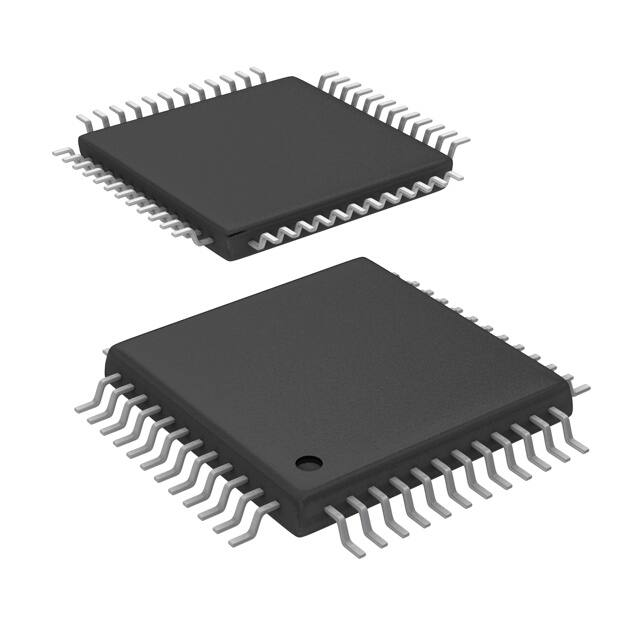
Connection Diagram
Figure 1. TOP VIEW
Block Diagram
2
Submit Documentation Feedback
Copyright © 2001–2013, Texas Instruments Incorporated
Product Folder Links: ADC10D040
�ADC10D040
www.ti.com
SNAS149G – OCT 2001 – REVISED MARCH 2013
PIN DESCRIPTIONS and EQUIVALENT CIRCUITS
Pin No.
Symbol
Equivalent Circuit
Description
48
47
I+
I−
Analog inputs to “I” ADC. With VREF = 1.4V, conversion range is
1.15V to 1.85V with GAIN pin low, or 0.8V to 2.2V with GAIN pin
high.
37
38
Q+
Q−
Analog inputs to “Q” ADC. With VREF = 1.4V, conversion range is
1.15V to 1.85V with GAIN pin low, or 0.8V to 2.2V with GAIN pin
high.
VREF
Analog Reference Voltage input. The voltage at this pin should be in
the range of 0.6V to 1.6V. With 1.4V at this pin and the GAIN pin
low, the full scale differential inputs are 1.4 VP-P. With 1.4V at this pin
and the GAIN pin high, the full scale differential inputs are 2.8 VP-P.
This pin should be bypassed with a minimum 1 µF capacitor.
45
VCMO
This is an analog output which can be used as a reference source
and/or to set the common mode voltage of the input. It should be
bypassed with a minimum of 1 µF low ESR capacitor in parallel with
a 0.1 µF capacitor. This pin has a nominal output voltage of 1.5V
and has a 1 mA output source capability.
43
VRP
Top of the reference ladder. Do not drive this pin. Bypass this pin
with a 10 µF low ESR capacitor and a 0.1 µF capacitor.
44
VRN
Bottom of the reference ladder. Do not drive this pin. Bypass this
pin with a 10 µF low ESR capacitor and a 0.1 µF capacitor.
1
Submit Documentation Feedback
Copyright © 2001–2013, Texas Instruments Incorporated
Product Folder Links: ADC10D040
3
�ADC10D040
SNAS149G – OCT 2001 – REVISED MARCH 2013
www.ti.com
PIN DESCRIPTIONS and EQUIVALENT CIRCUITS (continued)
Pin No.
Equivalent Circuit
Description
CLK
Digital clock input for both converters. The analog inputs are
sampled on the falling edge of this clock input.
OS
Output Bus Select. With this pin at a logic high, both the “I” and the
“Q” data are present on their respective 10-bit output buses (Parallel
mode of operation). When this pin is at a logic low, the “I” and “Q”
data are multiplexed onto the “I” output bus and the “Q” output lines
all remain at a logic low (multiplexed mode).
31
OC
Offset Correct pin. A low-to-high transition on this pin initiates an
independent offset correction sequence for each converter, which
takes 34 clock cycles to complete. During this time 32 conversions
are taken and averaged. The result is subtracted from subsequent
conversions. Each input pair should have 0V differential value during
this entire 34 clock period.
32
OF
Output Format pin. When this pin is LOW the output format is Offset
Binary. When this pin is HIGH the output format is 2's complement.
This pin may be changed asynchronously, but this will result in
errors for one or two conversions.
STBY
Standby pin. The device operates normally with a logic low on this
and the PD (Power Down) pin. With this pin at a logic high and the
PD pin at a logic low, the device is in the standby mode where it
consumes just 30 mW of power. It takes just 800 ns to come out of
this mode after the STBY pin is brought low.
35
PD
Power Down pin that, when high, puts the converter into the Power
Down mode where it consumes just 1 mW of power. It takes less
than 1 ms to recover from this mode after the PD pin is brought low.
If both the STBY and PD pins are high simultaneously, the PD pin
dominates.
36
GAIN
This pin sets the internal signal gain at the inputs to the ADCs. With
this pin low the full scale differential input peak-to-peak signal is
equal to VREF. With this pin high the full scale differential input peakto-peak signal is equal to 2 x VREF.
I0–I9 and Q0–Q9
3V TTL/CMOS-compatible Digital Output pins that provide the
conversion results of the I and Q inputs. I0 and Q0 are the LSBs, I9
and Q9 are the MSBs. Valid data is present just after the rising edge
of the CLK input in the Parallel mode. In the multiplex mode, Ichannel data is valid on I0 through I9 when the I/Q output is high
and the Q-channel data is valid on I0 through I9 when the I/Q output
is low.
28
I/Q
Output data valid signal. In the multiplexed mode, this pin transitions
from low to high when the data bus transitions from Q-data to I-data,
and from high to low when the data bus transitions from I-data to Qdata. In the Parallel mode, this pin transitions from low to high as the
output data changes.
40, 41
VA
Positive analog supply pin. This pin should be connected to a quiet
voltage source of +3.0V to +3.6V. VA and VD should have a common
supply and be separately bypassed with 10 µF to 50 µF capacitors in
parallel with 0.1 µF capacitors.
4
VD
Digital supply pin. This pin should be connected to a quiet voltage
source of +3.0V to +3.6V. VA and VD should have a common supply
and be separately bypassed with 10 µF to 50 µF capacitors in
parallel with 0.1 µF capacitors.
6, 30
VDR
Digital output driver supply pins. These pins should be connected to
a voltage source of +1.5V to VD and be bypassed with 10 µF to 50
µF capacitors in parallel with 0.1 µF capacitors.
3, 39, 42,
46
AGND
The ground return for the analog supply. AGND and DGND should
be connected together close to the ADC10D040 package.
5
DGND
The ground return for the digital supply. AGND and DGND should be
connected together close to the ADC10D040 package.
7, 29
DR GND
33
2
34
8 thru 27
4
Symbol
The ground return of the digital output drivers.
Submit Documentation Feedback
Copyright © 2001–2013, Texas Instruments Incorporated
Product Folder Links: ADC10D040
�ADC10D040
www.ti.com
SNAS149G – OCT 2001 – REVISED MARCH 2013
These devices have limited built-in ESD protection. The leads should be shorted together or the device placed in conductive foam
during storage or handling to prevent electrostatic damage to the MOS gates.
Absolute Maximum Ratings (1) (2) (3)
Positive Supply Voltages
3.8V
−0.3V to (VA or VD +0.3V)
Voltage on Any Pin
Input Current at Any Pin (4)
Package Input Current
±25 mA
(4)
±50 mA
Package Dissipation at TA = 25°C
See
ESD Susceptibility (6)
Human Body Model
2500V
Machine Model
250V
Soldering Temperature, Infrared, 10 sec.
235°C
−65°C to +150°C
Storage Temperature
(1)
(2)
(3)
(4)
(5)
(6)
(5)
All voltages are measured with respect to GND = AGND = DGND = 0V, unless otherwise specified.
Absolute Maximum Ratings indicate limits beyond which damage to the device may occur. Operating Ratings indicate conditions for
which the device is functional, but do not ensure specific performance limits. For ensured specifications and test conditions, see the
Electrical Characteristics. The ensured specifications apply only for the test conditions listed. Some performance characteristics may
degrade when the device is not operated under the listed test conditions.
If Military/Aerospace specified devices are required, please contact the Texas Instruments Sales Office/ Distributors for availability and
specifications.
When the input voltage at any pin exceeds the power supplies (VIN < GND or VIN > VA or VD), the current at that pin should be limited to
25 mA. The 50 mA maximum package input current rating limits the number of pins that can safely exceed the power supplies with an
input current of 25 mA to two.
The absolute maximum junction temperature (TJmax) for this device is 150°C. The maximum allowable power dissipation is dictated by
TJmax, the junction-to-ambient thermal resistance (θJA), and the ambient temperature (TA), and can be calculated using the formula
PDMAX = (TJmax - TA )/θJA. In the 48-pin TQFP, θJA is 76°C/W, so PDMAX = 1,645 mW at 25°C and 855 mW at the maximum
operating ambient temperature of 85°C. Note that the power dissipation of this device under normal operation will typically be about 307
mW (267 mW quiescent power + 40 mW due to 1 LVTTL load on each digital output). The values for maximum power dissipation listed
above will be reached only when the ADC10D040 is operated in a severe fault condition (e.g. when input or output pins are driven
beyond the power supply voltages, or the power supply polarity is reversed). Obviously, such conditions should always be avoided.
Human body model is 100 pF capacitor discharged through a 1.5 kΩ resistor. Machine model is 220 pF discharged through 0Ω.
Operating Ratings (1) (2)
−40°C ≤ TA ≤ +85°C
Operating Temperature Range
VA, VD Supply Voltage
+3.0V to +3.6V
VDR Supply Voltage
VIN Differential Voltage Range
VCM Input Common Mode Range
+1.5V to VD
GAIN = Low
±VREF
GAIN = Low
VREF/4 to (VA–VREF/4)
GAIN = High
VREF/2 to (VA–VREF/2)
VREF Voltage Range
0.6V to 1.8V
−0.3V to (VA +0.3V)
Digital Input Pins Voltage Range
(1)
(2)
±VREF/2
GAIN = High
Absolute Maximum Ratings indicate limits beyond which damage to the device may occur. Operating Ratings indicate conditions for
which the device is functional, but do not ensure specific performance limits. For ensured specifications and test conditions, see the
Electrical Characteristics. The ensured specifications apply only for the test conditions listed. Some performance characteristics may
degrade when the device is not operated under the listed test conditions.
All voltages are measured with respect to GND = AGND = DGND = 0V, unless otherwise specified.
Submit Documentation Feedback
Copyright © 2001–2013, Texas Instruments Incorporated
Product Folder Links: ADC10D040
5
�ADC10D040
SNAS149G – OCT 2001 – REVISED MARCH 2013
www.ti.com
Converter Electrical Characteristics
The following specifications apply for VA = VD = +3.3 VDC, VDR = +2.5 VDC, VREF = 1.4 VDC, GAIN = OF = 0V, OS = 3.3V, VIN
(a.c. coupled) = FSR = 1.4 VP-P, CL = 15 pF, fCLK = 40 MHz, 50% Duty Cycle, RS = 50Ω, trc = tfc < 4 ns, NOT offset corrected.
Boldface limits apply for TA = TMIN to TMAX: all other limits TA = 25°C (1)
Symbol
Parameter
Limits (3)
Units
(Limits)
±0.65
±1.9
LSB (max)
±0.35
+1.2
−1.0
LSB (max)
LSB (min)
10
Bits
Typical (2)
Conditions
STATIC CONVERTER CHARACTERISTICS
INL
Integral Non-Linearity
DNL
Differential Non-Linearity
Resolution with No Missing Codes
VOFF
GE
Without Offset Correction
−3.3
+7
−12
LSB (max)
LSB (min)
With Offset Correction
+0.4
+1.5
−0.5
LSB (max)
LSB (min)
−4
+5
−12
%FS (max)
%FS (min)
9.1
Bits (min)
Offset Error
Gain Error
DYNAMIC CONVERTER CHARACTERISTICS
ENOB
SINAD
SNR
THD
HS2
HS3
SFDR
IMD
FPBW
(1)
(2)
(3)
6
fIN = 4.43 MHz, VIN = FSR −0.1 dB
9.5
fIN = 10.4 MHz, VIN = FSR −0.1 dB, TA = 25°C
9.5
fIN = 19.7 MHz, VIN = FSR −0.1 dB
9.4
fIN = 4.43 MHz, VIN = FSR −0.1 dB
59
fIN = 10.4 MHz, VIN = FSR −0.1 dB, TA = 25°C
59
fIN = 19.7 MHz, VIN = FSR −0.1 dB
58
dB
fIN = 4.43 MHz, VIN = FSR −0.1 dB
60
dB
fIN = 10.4 MHz, VIN = FSR −0.1 dB, TA = 25°C
60
fIN = 19.7 MHz, VIN = FSR −0.1 dB
59
dB
fIN = 4.43 MHz, VIN = FSR −0.1 dB
−70
dB
fIN = 10.4 MHz, VIN = FSR −0.1 dB, TA = 25°C
−69
fIN = 19.7 MHz, VIN = FSR −0.1 dB
−67
dB
fIN = 4.43 MHz, VIN = FSR −0.1 dB
−86
dB
fIN = 10.4 MHz, VIN = FSR −0.1 dB
−83
dB
fIN = 19.7 MHz, VIN = FSR −0.1 dB
−81
dB
fIN = 4.43 MHz, VIN = FSR −0.1 dB
−73
dB
fIN = 10.4 MHz, VIN = FSR −0.1 dB
−73
dB
fIN = 19.7 MHz, VIN = FSR −0.1 dB
−72
dB
fIN = 4.43 MHz, VIN = FSR −0.1 dB
72
dB
fIN = 10.4 MHz, VIN = FSR −0.1 dB
72
dB
fIN = 19.7 MHz, VIN = FSR −0.1 dB
70
dB
Intermodulation Distortion
fIN1 < 8.5 MHz, VIN = FSR −6.1 dB
fIN2 < 9.5 MHz, VIN = FSR −6.1 dB
71
dB
Overrange Output Code
(VIN+−VIN−) > 1.5V
Underrange Output Code
(VIN+−VIN−) < −1.5V
Effective Number of Bits
Signal-to-Noise Plus Distortion Ratio
Signal-to-Noise Ratio
Total Harmonic Distortion
Second Harmonic
Third Harmonic
Spurious Free Dynamic Range
Full Power Bandwidth
Bits
Bits
dB
56.3
57.3
−61
dB (min)
dB (min)
dB (min)
1023
0
140
MHz
The inputs are protected as shown below. Input voltage magnitude up to 300 mV beyond the supply rails will not damage this device.
However, errors in the A/D conversion can occur if the input goes beyond the limits given in these tables.
Typical figures are at TJ = 25°C, and represent most likely parametric norms.
Test limits are specified to TI's AOQL (Average Outgoing Quality Level). Performance is specified only at VREF = 1.4V and a clock duty
cycle of 50%. The limits for VREF and clock duty cycle specify the range over which reasonable performance is expected. Tests are
performed and limits specified with clock low and high levels of 0.3V and VD−0.3V, respectively.
Submit Documentation Feedback
Copyright © 2001–2013, Texas Instruments Incorporated
Product Folder Links: ADC10D040
�ADC10D040
www.ti.com
SNAS149G – OCT 2001 – REVISED MARCH 2013
Converter Electrical Characteristics (continued)
The following specifications apply for VA = VD = +3.3 VDC, VDR = +2.5 VDC, VREF = 1.4 VDC, GAIN = OF = 0V, OS = 3.3V, VIN
(a.c. coupled) = FSR = 1.4 VP-P, CL = 15 pF, fCLK = 40 MHz, 50% Duty Cycle, RS = 50Ω, trc = tfc < 4 ns, NOT offset corrected.
Boldface limits apply for TA = TMIN to TMAX: all other limits TA = 25°C (1)
Symbol
Parameter
Conditions
Typical (2)
Limits (3)
Units
(Limits)
INTER-CHANNEL CHARACTERISTICS
Crosstalk
1 MHz input to tested channel, 10.3 MHz input to
other channel
−72
dB
Channel - Channel Aperture Delay
Match
fIN = 8 MHz
8.5
ps
0.1
%FS
Gain Pin = AGND
1.4
VP-P
Gain Pin = VA
Channel - Channel Gain Matching
REFERENCE AND ANALOG CHARACTERISTICS
VIN
Analog Differential Input Range
CIN
Analog Input Capacitance (each
input)
RIN
2.8
VP-P
Clock High
6
pF
Clock Low
3
pF
Analog Differential Input Resistance
13.5
kΩ
VREF
Reference Voltage
1.4
IREF
Reference Input Current


 工商网监
湘ICP备2023018690号
工商网监
湘ICP备2023018690号
