January 3, 2008
Rev – 1.1/CC
RoHS Compliant
National Semiconductor
Evaluation Board User's Guide
I2C-Compatible, 12-Bit, 10-Bit, or 8-Bit
Analog-to-Digital Converter (ADC) with Alert Function
12-bit
10-bit
8-bit
ADC121C021
ADC101C021
ADC081C021
ADC121C027
ADC101C027
ADC081C027
ALERT Option
ADDRESS Option
NOTE: The Evaluation Board is shipped with the Alert Option of the ADC. To
evaluate the Address Option, please order samples from www.national.com.
�Table of Contents
1.0 Introduction ............................................................................................................................3
2.0 Board Assembly .....................................................................................................................4
3.0 Quick Start .............................................................................................................................5
3.1 Stand Alone Mode.....................................................................................................5
3.2 Computer Mode ........................................................................................................5
4.0 Functional Description............................................................................................................6
4.1 Jumper Settings ........................................................................................................6
4.2 Analog Input Signal ...................................................................................................7
4.3 ADC Reference Circuitry...........................................................................................7
2
4.4 I C Interface ..............................................................................................................7
4.5 Alert Function ............................................................................................................7
4.6 Automatic Conversion Mode .....................................................................................8
4.7 Power Supply Connections .......................................................................................8
5.0 Software Operation and Settings ...........................................................................................8
5.1 Software Quick Start .................................................................................................8
5.2 Data Analysis ............................................................................................................9
5.3 Register Control ........................................................................................................10
5.4 Troubleshooting WaveVision ....................................................................................11
6.0 Evaluation Board Specifications ............................................................................................12
7.0 Test Points, Connectors, and Jumpers..................................................................................12
8.0 Hardware Schematic..............................................................................................................13
9.0 Evaluation Board Layers ........................................................................................................14
10.0 Evaluation Board Bill of Materials ........................................................................................15
2
http://www.national.com
�1.0 Introduction
This Design Kit (consisting of the ADC Evaluation
Board and this User's Guide) is designed to ease
evaluation
and
design-in
of
National
Semiconductor’s ADC121C021 family of Analogto-Digital Converters. The ADCs can operate at
speeds up to 188.9 kSPS. The converter features
2
an I C interface and an Alert function. This User’s
Guide supports all three resolutions and both
package options of the ADC121C021 ADC family.
All the devices in the family (ADC121C021,
ADC121C027,
ADC101C021,
ADC101C027,
ADC081C021, and ADC081C027) will be referred
to as the ADC121C021 in this document. The
ADCXX1C021 options offer an ALERT output pin,
whereas, the ADCXX1C027 offers an address
selection pin. The board comes stuffed with the
ALERT option (ADCXX1C021). To evaluate the
Address Option (ADCXX1C027) with this board,
please go to www.national.com and order
samples. Use care when de-soldering the ADC to
ensure the pads of U3 are not damaged.
The evaluation board can be used in either of two
modes. In Stand Alone, suitable test equipment
such as a logic analyzer with a pattern generator
can be used with the board to evaluate the
ADC121C021’s performance.
JP1: INPUT
SELECT
In the Computer mode, data capture and
evaluation are simplified by connecting the
evaluation board to National Semiconductor's
WaveVision 4 Data Capture Board (order number
WAVEVSN BRD 4.1 or higher) which connects to
a personal computer through a USB port and runs
WaveVision 4 software revision 4.4 or higher.
The latest version of the WaveVision 4 software
should be downloaded from the web at
http://www.national.com/adc.
Note: WaveVision software version 4.4 or higher
is required to evaluate this part with the WV4
Evaluation System.
The WaveVision 4 software operates under
Microsoft Windows. The signal at the analog
input is digitized, captured, and displayed on a PC
monitor in the time and frequency domains.
The software will perform an FFT on the captured
data upon command. This FFT plot shows the
dynamic performance in the form of SNR, SINAD,
THD, SFDR, and ENOB. A software histogram of
the captured data is also available. WaveVision
also provides control of the ADC’s internal
registers through the WaveVision4 software.
The signal at analog input J2 is digitized by U3,
the ADC121C021.
U3: ADC
[ADC121C021]
2
JP2: I C PULL-UP
Enable
J2: INPUT
U2: AMP
[LMP7731]
J1: WV4S
Connector
JP5: VA
SELECT
JP7: 4.1V
REF Enable
U5: REF
[LM4050-4.1]
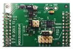
Figure 1: Component Locations
3
http://www.national.com
�2.0 Board Assembly
The ADC121C02XEB evaluation board comes
fully assembled and ready for use. The provided
jumpers are in their recommended locations and
suit the needs of most users. Refer to the Bill of
Materials for a description of components, to
Figure 1 for major component placement, and to
Figure 10 for the evaluation board schematic.
While the board has been populated in a manner
that is most advantageous for typical usage, the
board can be customized by adding components
to meet the user’s specific needs. The board
comes ready to use with a DC coupled input
signal (Figure 2). However, by adding DC bias
resistors R1 and R4 (value 4.99kΩ), and changing
C1 to a 1.0uF capacitor, the board can be used
with an AC coupled input signal (Figure 3).
Figure 2: DC Coupled Input Configuration
If needed, the input can be terminated by adding
an appropriate termination resistor at R3. The
V_IN footprint (J2) has been stuffed with a singlepin header for testing typical, slow-moving DC
input signals. An SMA footprint is also included
on the PCB and should be used for precise
dynamic performance evaluation. The Bill of
Materials (Section 10) lists an appropriate SMA
connector to use.
The LMP7731 Low-noise, Precision Operational
Amplifier is included on the ADC121C02XEB for
convenient buffering of the analog input. By
default, it is configured as a simple voltage
follower (Figure 4). Resistors R10 and R11 can
be modified to add non-inverting gain to the
circuit. Adding capacitance at C6 configures the
amplifier as a low-pass filter. To incorporate the
input buffer into the signal path, short pins 2 and 3
of JP1.
Figure 4: Input Buffer Configuration
Figure 3: AC Coupled Input Configuration
4
http://www.national.com
�The LM4050-4.1 Precision, Micropower, Shunt
Voltage Reference is
included on the
ADC121C02XEB as a clean reference solution for
the ADC.
To evaluate the ADC using the
LM4050, simply short pins 1 & 2 of JP7, and move
the VA_SELECT jumper to pins 7 & 8 of JP5
(Figure 5).
Figure 5: LM4050 Jumper Configuration
3.0 Quick Start
The ADC121C02XEB evaluation board may be
used in the Stand Alone mode to capture data
with a logic analyzer or third party equipment, or it
may be used in the Computer Mode with a
WaveVision 4 Data Capture Board, referenced
throughout the remainder of this document as
WV4. In both cases, the data may be analyzed
with the WaveVision software.
3.1 Stand Alone Mode
Refer to Figure 1 for locations of test points and
major components.
2
1. The I C interface signals (SCL and SDA) may
be driven directly at J1 or with wires soldered
to VIA1 and VIA2 (step 7). A fully-compliant
2
I C interface analyzer should be used to drive
SCL and SDA while monitoring the data
output (SDA).
2. The board provides the option of adding 2kΩ
2
pull-up resistors to the I C bus, SCL and SDA.
To enable the pull-up resistors, short pins 1 &
2
2 of JP2. Assuming the I C analyzer has
built-in pull-up resistors, the jumper at JP2
must be removed to disable the on-board pull2
up resistors. If the I C analyzer doesn’t have
built-in pull-up capability, leave JP2 shorted.
3. Connect a clean analog (not switching) +5.0V
power source with a 300mA current limit to
power connector TP7. Ground TP6.
5
4. Move the shorting jumper at JP5 to pins 9 &
10. NOTE: only two consecutive pins may be
shorted on JP5 at a time.
5. Turn on the power supply.
6. Connect the input signal to the test-point at
J2. The input signal return can be connected
to ground at TP3. Please note the evaluation
board is assembled for a DC-coupled input
source. The board is designed for an AC
coupled input as well. Modifying the board for
an AC coupled input is described above in
Section 2.0. If the source has a 50 ohm output
impedance, install a 51 ohm resistor at R3.
To accurately evaluate the dynamic
performance of the ADC121C021, the source
must be better than 90dB THD.
7. If evaluating the ADC121C027, configure the
2
I C slave address. The address is controlled
by VIA5. With VIA5 left floating, the slave
address of the ADC121C027 will be set to
50hex. Grounding VIA5 sets the address to
51hex. Connecting VIA5 to VA sets the
address to 52hex.
8. If evaluating the ADC121C021, the slave
address is permanently set to 54hex.
9. If evaluating the ADC121C021, the ALERT
pin can be monitored at VIA5.
3.2 Computer Mode
Refer to Figure 1 for locations of test points and
major components. The board comes configured
for “plug-and-play” WaveVision evaluation.
1. Run the WaveVision 4 program, version 4.4 or
higher is required to interface to the WV4
board. While the program is loading, continue
below.
2. Connect a USB cable between the WV4
board and the PC running the WaveVision 4
software.
3. Make
the
following
required
jumper
connections, see table 1 for more details:
• JP1 - pins 1 & 2
• JP2 - pins 1 & 2
• JP5 - pins 3 & 4 (All other pins of JP5
must be left open)
http://www.national.com
�4. Connect the J1 header on the ADC121C021
evaluation board to the WV4 serial connector
(J7) on the WV4 board. Refer to Figure 6 for
the serial connection and Figure 7 for the J1
header pin out.
7. Refer to Section 5.0 on Software Operation
and Settings to setup the WaveVision 4
software.
4.0 Functional Description
4.1 Jumper Settings
Table 1 describes the function of the various
jumpers on the ADC121C021 evaluation board.
The evaluation board schematic is shown in
Figure 10.
Pins 1 & 2
Pins 2 & 3
Select direct VIN
circuit
Select Amplified VIN
circuit [LMP7731]
Jumper
JP1
JP2
Enable I2C Pull-up resistors
JP3
Permanently shorted
JP5
VA SELECT (See Below)
JP6
Not Used
Figure 6: WV4 to ADC121C02XEB Connection
JP7
SDA
(ADC)
1
Enable 4.1V Shunt Reference
[LM4050-4.1]
2
GND
Jumper JP5 (VA SELECT)
3
4
SDA
(ADC)
5
6
7
8
N/C
SCL
11
12
Select 5.0V supply from WV4S connector.
Pins 5 & 6
Not Used
Pins 7 & 8
Select 4.1V shunt reference supply.
[LM4050-4.1]
Pins 9 & 10
Select external supply from TP7.
(EEPROM)
+3.3V
13
Pins 3 & 4
10
SDA
(EEPROM)
Select 3.3V regulated supply from WV4S
connector.
[LM1117MPX-3.3 on the WV4 board]
GND
N/C
9
Pins 1 & 2
14
+5V
Table 1: Jumper Configurations
Figure 7: J1 (WV4S) Header Pin Out
5. Perform step 6 of section 3.1 to drive the
analog input. For information on changing the
configuration of the analog input section, read
Section 2.0 Board Assembly for details. The
board comes ready for a DC coupled input
signal.
6. Connect a clean (not switching) +5.0V power
source with a 350mA current limit to power
connector J1 on the WV4 board. Turn on the
power supply.
6
http://www.national.com
�4.2 Analog Input Signal
4.3 ADC Reference Circuitry
There are three basic options for connecting an
input signal to the ADC. The three options
facilitate AC-coupled and DC-coupled input
signals.
The ADC121C021 family is internally referenced.
Therefore, the Analog-to-Digital converter gets its
reference from the analog supply (VA). Hence, a
clean analog supply must be used to guarantee
the performance of the ADC.
The first way to apply an input signal to the ADC
is to connect it to pin 2 of JP1. The signal’s return
(GND) should be connected to TP5.
This
configuration provides the input circuit seen in
Figure 8.
2
4.4 I C Interface
Please refer to section 1.7 of the ADC121C021
2
datasheet for a detailed description of the I C
interface.
2
The board is designed with I C pull-up resistors on
both the SDA and SCL lines (R8 & R9). These
resistors are enabled by a single jumper (JP2)
2
and can easily be added or removed from the I C
bus. Also, footprints for series resistors are
designed into the board (R2 & R5). The board is
shipped with 0Ω resistors which can be modified
to provide series resistance if interfacing to a
2
noisy I C bus.
Figure 8: Unbiased input circuit.
The second way is to configure the board for an
AC coupled input. DC biasing is available for
inputs applied to J2 but is currently not populated
on the board. By adding DC bias resistors R1 and
R4 (value 4.99kΩ), and changing C1 to a 1.0uF
capacitor, the board can be used with an AC
coupled input signal (Figure 3). To improve the
signal integrity of the connection to the board, an
SMA connector should be stuffed at J2 (V_IN). If
the input source has a 50Ω output impedance, a
51Ω resistor can be installed at R3.
The third way to configure the input is by
incorporating the Amplifier into the signal path.
The LMP7731 Low-noise, Precision Operational
Amplifier is included on the board for convenient
buffering of the analog input. By default, it is
configured as a simple voltage follower (Figure 4).
Resistors R10 and R11 can be modified to add
non-inverting gain to the circuit.
Adding
capacitance at C6 configures the amplifier as a
low-pass filter. To use the input buffer, simply
move the JP1 jumper to pins 2 & 3.
In any case, it is important that the signal stays
within the allowable input range of the ADC (0V to
VA). Dynamic input signals should be applied
through a bandpass filter to eliminate the noise
and harmonics commonly associated with signal
sources. To accurately evaluate the performance
of the ADC121C021, the source must be better
than -90dBc THD.
7
The SDA signal is accessible by soldering to VIA1
or connecting to pin 1 of the WV4S connector
(J1). The SCL signal is accessible by soldering to
VIA2 or connecting to pin 5 of J1.
The on-board pull-up resistors can be powered
with an external supply by removing the jumper at
JP2 and connecting the supply to pin 2 of JP2 or
VIA6.
4.5 Alert Function
The ADC121C021 provides a programmable “outof-range” Alert function. At the end of every
conversion, the measured voltage is compared to
the values in the VHIGH and VLOW registers. If the
measured voltage violates either of these values,
an alert condition occurs. The Over Range Alert
flag in the Alert Status Register indicates the VHIGH
limit has been violated. The Under Range Alert
flag indicated the VLOW limit has been violated. If
enabled, the alert condition is also propagated to
bit15 of the Conversion Result Register and the
ALERT output pin.
The Alert function is configured by writing to the
ADC’s internal registers. Refer to Section 1.6 of
the Datasheet for a detailed description of the
ADC’s internal Registers.
Refer to Section 1.8 of the Datasheet for a
detailed description of the Alert function.
http://www.national.com
�4.6 Automatic Conversion Mode
The Automatic Conversion Mode configures the
ADC to continually perform conversions without
2
receiving “read” instructions from the I C
controller. It is activated by writing a non-zero
value into the Cycle Time bits “D[7:5]” of the
Configuration
Register.
Various
automatic
conversion rates are supported.
Refer to Section 1.9 of the Datasheet for a
detailed description of the Automatic Conversion
Mode.
4.7 Power Supply Connections
The analog supply voltage (VA) can range from
+2.7V to +5.5V. The Evaluation system provides a
handful of power supply options via the JP5
header (see Table 1). VA can be driven by the
LM4050-4.1 Shunt Reference, the LM1117MPX3.3 LDO from the WV4 board, or an external
supply. National recommends the LM4050
precision reference for the ADC121C021.
NOTE: In Computer mode, if VA is driven with less
than 3.3V in Computer mode, an external 3.3V
pull-up supply is needed. This will ensure the
3.3V CMOS logic thresholds of the WaveVision4
board are met for SDA and SCL.
To use an external pull-up supply, remove the
jumper at JP2 and connect the supply to pin 2 of
JP2 or VIA6. An external pull-up supply will also
improve the dynamic performance of the ADC.
Typical supply currents when applying an external
supply to TP7 (VA_EXT) and performing ADC
conversions are as follows:
• For VA = +3.3V, I = 8mA
• For VA = +5.0V, I = 11mA
When operating in Stand Alone mode, always use
an external supply. Apply a +5.0V power source
with a current limit of 100mA to TP7, ground TP6,
and place a shorting jumper across pins 9 & 10 of
JP5.
Note: The +3.3V required to power the EEPROM
(U4) is obtained through J2 from the WV4 board.
The EEPROM is used to identify the type of Eval
Board connected to the WaveVision system in
Computer Mode.
5.0 Software Operation and Settings
The WaveVision 4 software is included with the
WV4 board and the latest version can be
downloaded for free from National's web site at
http://www.national.com/adc.
WaveVision4
software version 4.4 or later is required to
evaluate this device with the WaveVision system.
5.1 Software Quick Start
To install this software, follow the procedure in the
WV4 Board User's Guide. Once the software is
installed, run and set it up as follows:
1. Connect the WV4 board to the host computer
with a USB cable.
2. From the WaveVision main menu, go to
Settings and then Capture Settings to open
the System Settings window (Figure 9) and
select the following:
• WaveVision 4 (USB)
• Number of Samples: 2k to 128k, as
desired
• Data Format: Binary
Note: A majority of this current is for powering
devices external to the ADC121C021 such as the
pull-up resistors and the input amplifier.
When operating in the computer mode, the supply
voltage for VA can be applied externally or
supplied directly by the WV4 board through J1.
The external supply voltage is selected by placing
a jumper across pins 9 & 10 of JP5, applying a
power source with a 300mA current limit to TP7,
and grounding TP6. To use the 5.0V supply
directly from the WV4 board, place a shorting
jumper across pins 3 & 4 of JP5. To use the 3.3V
supply directly from the WV4 board, place a
shorting jumper across pins 1 & 2 of JP5. To use
the LM4050 4.1V Shunt Reference, place a
shorting jumper across pins 7 & 8 of JP5. For the
best performance, use a clean external supply.
8
Figure 9: System Settings window
http://www.national.com
�3. Apply power as specified in Section 4.4, click
on the "Reset" button and await the firmware
to download.
4. Click on the "Close" button to close the
System Settings window.
5. Navigate to the ADC121C021 Eval Board
Window. This is the Control Panel for the
device (Figure 10).
2
7. Set the I C Slave Address (Figure 10). The
address will default to the correct address for
the ADC121C021 (54hex). If evaluating the
2
ADC121C027, the I C address must be
changed to reflect the state of the address
selection pin (ADDR).
8. Press the “Read Registers” button. All of the
register fields will update (Figure 10).
9. Configure the ADC’s internal registers. The
Alert function and Automatic Conversion
Mode are setup through the Configuration
register. After making changes to a register
value, press the Enter key to write the register
(Figure 10).
10. To capture a dataset from the ADC, navigate
back to the main WaveVision window.
11. After the steps outlined in Section 3.2 are
completed, click on ‘Acquire’ then ‘Samples’
from the Main Menu (you can also press the
F1 shortcut key). If a dialog box opens, select
‘Discard’ or press the Escape (Esc) key to
start collecting new samples.
5.2 Data Analysis
WaveVision main menu will display an output plot.
Make sure there is no clipping of data samples.
Click on the software histogram tab and ensure
data does not exceed the limits of the device. The
samples may be further analyzed by clicking on
the magnifying glass icon, then clicking and
dragging across a specific area of the plot for
better data inspection (Figure 12).
See the
WaveVision 4 Board User's Guide for more
details.
Figure 10: ADC121C021 Control Panel
2
6. Select the desired I C Speed from the pulldown menu (Figure 11).
Figure 11: ADC121C021 Control Panel
Figure 12: Software Histogram: Sine Wave Input
9
http://www.national.com
�To view an FFT of the data captured, click on the
‘FFT’ tab. This plot may be zoomed in on the data
plot. A display of dynamic performance
parameters in the form of SINAD, SNR, THD,
SFDR and ENOB will be displayed at the top right
hand corner of the FFT plot (Figure 13).
5.3 Register Control
The ADC’s internal registers are controlled
through the ADC121C021 Control Panel
(see Figure 7). WaveVision allows both read and
write access to these registers. To read the
registers, simply click the “Read All” button in the
Control Panel window. Each of the registers is
read and displayed in the control panel. To write
to a register, simply type in the 8-bit or 16-bit hex
value to be written to the register and press Enter.
All hex values are assumed to be right justified.
Zeros are written to unspecified bits.
Many functions of the ADC121C021 are enabled
through the internal registers. Please refer to
Section 1.6 on Internal Registers in the Datasheet
for further details.
For example, the following steps will enable the
ALERT pin, set the VLOW threshold to ¾ full-scale,
and create an Under Range Alert condition.
Figure 13: FFT: 1kHz Sine Wave Input
Acquired data may be saved to a file. Plots may
also be exported as graphics. See the Data
Capture Board User's Guide for details.
10
-Write 0x04 to the Configuration register.
-Write 0xBFF to the VLOW register.
-Ground the analog input (VIN).
-Click the “Read Registers” button to read all the
registers.
-The Alert Status register will read 01hex to
indicate that the VLOW value was violated and an
Under Range Alert condition has occurred.
http://www.national.com
�5.4 Troubleshooting WaveVision
5.4.1 Problems
5.4.2 Solutions
Problem 1: The “ADC121C021 Eval Board”
Control Panel appears briefly, but disappears after
powering on the WaveVision board. Try Solutions
A, B, and C. After trying these solutions, the
WaveVision system must be hard reset to
recover. Press SW1 on the WV4 board to reset
the system.
Solution A: Ensure power is supplied to the VA
supply on the board. A single jumper must be
placed across either pins 1&2, pins 3&4, pins 7&8,
or pins 9&10 of JP5 to select the board’s power
source. If using the Shunt Reference, pins 1&2 of
JP7 must be shorted. The VA supply is measured
by probing VIA10.
Problem 2: The following error occurs when I try
to acquire data samples. Try Solution D.
Solution B: Ensure the pull-up resistors are
powered (R8 and R9). In Computer mode, JP2
must be shorted by a jumper for the WaveVision
software to work properly.
Solution C: Ensure the board is firmly connected
to the WV4 board via the WV4S connector (J1).
See Figure 6.
2
Problem 3: The following error occurs when I try
to read or write registers through the Control
Panel. Try Solution D.
Problem 4: One of the following errors occurs
when I try to read or write registers through the
Control Panel. “java.lang.Exception: A USB
…CMD_REG_RW … while sending bulk read.”
Solution D: Ensure the I C Slave address is set
correctly in WaveVision.
If evaluating the
ADC121C021, the address must be set to 0x54.
If evaluating the ADC121C027, the address will
be 0x50 if no user modifications have been made
to the board and ADDR is floating. If ADDR is tied
to GND, the address must be set to 0x51. If
ADDR is tied to VA, the address must be set to
0x52.
Solution E: Ensure the 3P3V supply is connected
to the 3.3V regulated supply from the WV4 board.
The 3P3V supply is measured by probing pin 1 of
JP5. Test this with a volt-meter. The EEPROM
(U4) must be powered with 3.3V for WaveVision
to work properly.
“An exception occurred. Control Panel…”
Try Solutions A, B, and C. After trying these
solutions, the WaveVision system must be hard
reset to recover. Press SW1 on the WV4 board to
reset the system.
Problem 5: The Eval Board is not recognized
correctly in the System Settings Window (Figure
9). Try Solutions D and E.
11
http://www.national.com
�6.0 Evaluation Board Specifications
Board Size:
Power Requirements:
I2C Interface Speed:
Analog Input Range:
3.1" x 1.85" (7.9 cm x 4.6 cm)
Min: +2.7V,
Max: +5.5V,
10mA
13mA
100 kHz, 400kHz, or 3.4 MHz
GND to VA
7.0 Test Points, Connectors, and Jumpers
Test Points on the ADC121C021 Evaluation Board
TP2: AGND
Ground. Located at the center of the board.
TP3: AGND
Ground. Located at the top left of the board.
TP5: AGND
Ground. Located at the top middle of the board.
TP6: AGND
Ground. Located at the left side of the board.
TP7: VA_EXT
External Power supply input. Located at the left side of the board.
TP8: AGND
Ground. Located at the bottom right of the board.
TP9: WV_CLK_IN
Not Used.
TP10: AGND
Ground. Located at the right side of the board.
Connectors on the ADC121C021 Evaluation Board
J1: WV4S
14 pin dual row right angle male header: Connects to WV4 board.
J2: V_IN
Analog Input of the Eval Board.
Selection Jumpers on the ADC121C021 Evaluation Board (Refer to table 1 in Section 4.0 for configuration details)
JP1: V_IN SELECT
Selects buffered or unbuffered signal path.
JP2: V_PULL SELECT
Enables the on-board I2C pull-up resistors.
JP3: V+_AMP
Permanently shorted. Connects VA to the V+ supply of the Amplifier.
JP4: OSC_ENABLE
Not Used.
JP5: VA SELECT
Selects the VA source (See section 4.4)
JP6: CLK SELECT
Not Used.
JP7: VA_EXT_SHUNT
Enables the 4.1V Shunt Reference. Connects the 5P0V supply to the reference circuit.
JP8: VA_EXT_LDO
Not Used.
12
http://www.national.com
�AGND
VA
VIA7
JP3
I_AMP
V+_AMP
TP6
AGND
AGND
1
1
V(+)
Vin(-)
C6
R10
2
1
5P0V_WV
VA_EXT_SHUNT
JP7
U5
56
NS
0
Vout
V(-)
Vin(+)
LM4050-4.1
R16
4.1V SHUNT
REFERENCE
->57 mil inch pads
->37 mil inch drills
->100 mil inch spacing
Small Perf-board Area
R11
NS
0.1uF
C4
5
4
U2
LMP7731
R3
NS
C1
0 Ohm RES
1
2
3
R4
NS
R1
NS
VIA12
1
2
3
3
2
1
VA
VA
Vin
Vref
NS (LDO Reference)
EN
GND
NC
U6
TP7
VA_EXT
VA_EXT
V_IN SELECT
INPUT SELECT
JP1
L3
20
R6
C2
VIA10
ADR0
C7
0 Ohm R
10.0uF
NS
C11
4
5
3
2
1
VIA8
470pF
0.1uF
C12
VA
JP8
VA_EXT_LDO
5P0V_WV
SCL
4
5
6
VIA13
NS
ALR/ADR
VIA5
ALR/ADR
VIA11
5P0V_WV
ADR1
ALR
3P3V_WV
JP5
VA SELECT
0.1uF
C8
U3
VIN
GND
VA
AGND
SDA
TP2
AGND
U1
ADC121C021
3.3V LDO
REFERENCE
10
9
1
V_IN
V_IN
8
7
1
2
1
1
6
5
4
5
1
1
4
3
1
3
1
2
6
1
1
1
7
2
3
4
5
1
2
1
1
1
1
1
1
2
1
1
2
1
8
1
1
VA
TP8
AGND
AGND
1
1
AGND
TP5
AGND
R9
2K
3P3V_WV
V_PULL SELECT
V_PULL
2
1
R8
2K
NS
0
0
JP2
R7
R5
R2
1
1
VIA6
1
1
R17
1.0uF
C9
10.0uF
C3
VIA9
100uH
OUT
C10
0 Ohm R
NS
8
L1
0
R15 51
R19
R18
51
NS
3P3V_WV
WV4S
6
8
10
5
7
9
AGND
TP10
AGND
13
3P3V
SCL_EEPROM
WV4S
14
5P0V_WV
5P0V
NS
R13
0.1uF
C5
4
3
12
2
1
3P3V_WV
J1
AGND
SDATA
SCLK
WV_CLK_IN
TP9
VA_EXT
CLKSEND
JP4
CLKSEND
SCL
SDA
AGND
SCL
SDA_EEPROM 11
Y1
OSC (THROUGH-HOLE)
1
JP6
CLK SELECT
CLK SELECT
OE
100uH
L2
R12
VA
5P0V_WV
3
VIA4
VIA3
VIA2
VIA1
---
CSb
2
AGND
3
2
SDA
1
SPI
I2C
1
1
VIA
1
3
1
1
2
1
1
14
7
GND VDD
1
1
1
1
1
J2
1
1
1
1
8
VCC
6
A0
R14
3P3V_WV
NS
3P3V_WV
1
5
GND SDA
7
WP
A1
2
SCL
A2
3
1
1
13
4
TP3
AGND
EEPROM
U4
24C02
8.0 Hardware Schematic
Figure 10: ADC121C021 Evaluation Board Schematic
http://www.national.com
1
�9.0 Evaluation Board Layers
Figure 11: ADC121C021 Evaluation Board: All Layers with Silk Screen
Figure 12: ADC121C021 Evaluation Board: Top Layer
Figure 13: ADC121C021 Evaluation Board: Bottom Layer
14
http://www.national.com
�10.0 Evaluation Board Bill of Materials
Qty
Reference
Value
Description
1
C1
0 Ohm R
0 Ohm RES
1
2
C2
C3,C7
470pF
10.0uF
CAP
CAP
5
0.1uF
CAP
1
1
C4,C5,
C8,C12
C6,C11
C9
NS
1.0uF
CAP
CAP
1
1
C10
JP1
0 Ohm R
INPUT SELECT
0 Ohm RES
JUMPER
1
1
JP2
JP3
V_PULL
NS
JUMPER
JUMPER
1
1
JP4
JP5
NS
VA SEL
1
1
JP6
JP7
1
1
Source
Source Part #
Manufacturer
Digikey
511-1463-1-ND
Kemet
Digikey
A26513-40-ND
Digikey
A26513-40-ND
JUMPER
JUMPER
Digikey
A26529-40-ND
CLK SELECT
VA_EXT_SHUNT
JUMPER
JUMPER
Digikey
Digikey
A26513-40-ND
A26513-40-ND
JP8
J1
NS
WV4S
JUMPER
HEAD
Digikey
S5803-07-ND
1
J2
V_IN
TP
Center Via
of SMA
Digikey
5011K-ND
2
1
L1,L2
L3
100uH
0 Ohm R
IND
0 Ohm RES
Digikey
490-1056-1-ND
9
NS
RES
0
RES
1
R1,R3,R4,
R7,R11,
R13,R14,
R17,R18
R2,R5,
R10,R12
R6
20
RES
2
2
R8,R9
R15,R19
2K
51
RES
RES
1
1
R16
TP2
500
AGND
RES
TP
2
3
AGND
AGND
TP
TP
Digikey
Digikey
1
TP3,TP6
TP5,TP8,
TP10
TP7
VA_EXT
TP
Digikey
5011K-ND
Single-pin
Header
5011K-ND
1
1
TP9
U1
WV_CLK_IN
ADC121C021
TP
ADC -TSOT6
1
1
U2
U3
LMP7731
NS
AMP-SOT23-5
MSOP8
1
1
U4
U5
24C02
LM4050-4.1
U6
VIA1-13
NS
NS
Y1
OSC (Socket)
4
1
12
1
15
Manufacturer Part #
Sullins
PRPN072PARN-RC
Murata
BLM31PG121SN1L
NS
NS
NSC
ADC121C021CIMK
NSC
LMP7731MF
EEPROM
SHUNT REF
NSC
LM4050AIM3-4.1
LDO-SOT23-5
NSC
LM4132AMF-3.3
Aries
08-3518-10
Digikey
A400-ND
http://www.national.com
�BY USING THIS PRODUCT, YOU ARE AGREEING TO BE BOUND BY THE TERMS AND CONDITIONS OF NATIONAL
SEMICONDUCTOR'S END USER LICENSE AGREEMENT. DO NOT USE THIS PRODUCT UNTIL YOU HAVE READ AND
AGREED TO THE TERMS AND CONDITIONS OF THAT AGREEMENT. IF YOU DO NOT AGREE WITH THEM, CONTACT THE
VENDOR WITHIN TEN (10) DAYS OF RECEIPT FOR INSTRUCTIONS ON RETURN OF THE UNUSED PRODUCT FOR A
REFUND OF THE PURCHASE PRICE PAID, IF ANY.
The ADC121C02XEB, ADC101C02XEB, and ADC081C02XEB Evaluation Boards are intended for product evaluation purposes
only and are not intended for resale to end consumers, are not authorized for such use, and are not designed for compliance with
European EMC Directive 89/336/EEC, or for compliance with any other electromagnetic compatibility requirements.
National Semiconductor Corporation does not assume any responsibility for use of any circuitry or software supplied or described.
No circuit patent licenses are implied.
LIFE SUPPORT POLICY
NATIONAL'S PRODUCTS ARE NOT AUTHORIZED FOR USE AS CRITICAL COMPONENTS IN LIFE SUPPORT DEVICES OR
SYSTEMS WITHOUT THE EXPRESS WRITTEN APPROVAL OF THE PRESIDENT OF NATIONAL SEMICONDUCTOR
CORPORATION. As used herein:
1. Life support devices or systems are devices or systems
which, (a) are intended for surgical implant into the body,
or (b) support or sustain life, and whose failure to
perform, when properly used in accordance with
instructions for use provided in the labeling, can be
reasonably expected to result in a significant injury to the
user.
National Semiconductor Corporation
Americas
Tel:
1-800-272-9959
Fax: 1-800-737-7018
Email: support@nsc.com
National Semiconductor Europe
Fax: +49 (0) 1 80-530 85 86
Email: europe.support@nsc.com
Deutsch Tel: +49 (0) 699508 6208
English Tel: +49 (0) 870 24 0 2171
French Tel: +49 (0) 141 91 8790
2. A critical component is any component in a life support
device or system whose failure to perform can be
reasonably expected to cause the failure of the life
support device or system, or to affect its safety or
effectiveness.
National Semiconductor
Asia Pacific Customer
Response Group
Tel: 65-2544466
Fax: 65-2504466
Email:sea.support@nsc.com
National
Semiconductor
Japan Ltd.
Tel: 81-3-5639-7560
Fax: 81-3-5639-7507
www.national.com
National does not assume any responsibility for any circuitry described, no circuit patent licenses are implied and National reserves the right at any
time without notice to change said circuitry and specifications.
16
http://www.national.com
�EVALUATION BOARD/KIT/MODULE (EVM) ADDITIONAL TERMS
Texas Instruments (TI) provides the enclosed Evaluation Board/Kit/Module (EVM) under the following conditions:
The user assumes all responsibility and liability for proper and safe handling of the goods. Further, the user indemnifies TI from all claims
arising from the handling or use of the goods.
Should this evaluation board/kit not meet the specifications indicated in the User’s Guide, the board/kit may be returned within 30 days from
the date of delivery for a full refund. THE FOREGOING LIMITED WARRANTY IS THE EXCLUSIVE WARRANTY MADE BY SELLER TO
BUYER AND IS IN LIEU OF ALL OTHER WARRANTIES, EXPRESSED, IMPLIED, OR STATUTORY, INCLUDING ANY WARRANTY OF
MERCHANTABILITY OR FITNESS FOR ANY PARTICULAR PURPOSE. EXCEPT TO THE EXTENT OF THE INDEMNITY SET FORTH
ABOVE, NEITHER PARTY SHALL BE LIABLE TO THE OTHER FOR ANY INDIRECT, SPECIAL, INCIDENTAL, OR CONSEQUENTIAL
DAMAGES.
Please read the User's Guide and, specifically, the Warnings and Restrictions notice in the User's Guide prior to handling the product. This
notice contains important safety information about temperatures and voltages. For additional information on TI's environmental and/or safety
programs, please visit www.ti.com/esh or contact TI.
No license is granted under any patent right or other intellectual property right of TI covering or relating to any machine, process, or
combination in which such TI products or services might be or are used. TI currently deals with a variety of customers for products, and
therefore our arrangement with the user is not exclusive. TI assumes no liability for applications assistance, customer product design,
software performance, or infringement of patents or services described herein.
REGULATORY COMPLIANCE INFORMATION
As noted in the EVM User’s Guide and/or EVM itself, this EVM and/or accompanying hardware may or may not be subject to the Federal
Communications Commission (FCC) and Industry Canada (IC) rules.
For EVMs not subject to the above rules, this evaluation board/kit/module is intended for use for ENGINEERING DEVELOPMENT,
DEMONSTRATION OR EVALUATION PURPOSES ONLY and is not considered by TI to be a finished end product fit for general consumer
use. It generates, uses, and can radiate radio frequency energy and has not been tested for compliance with the limits of computing
devices pursuant to part 15 of FCC or ICES-003 rules, which are designed to provide reasonable protection against radio frequency
interference. Operation of the equipment may cause interference with radio communications, in which case the user at his own expense will
be required to take whatever measures may be required to correct this interference.
General Statement for EVMs including a radio
User Power/Frequency Use Obligations: This radio is intended for development/professional use only in legally allocated frequency and
power limits. Any use of radio frequencies and/or power availability of this EVM and its development application(s) must comply with local
laws governing radio spectrum allocation and power limits for this evaluation module. It is the user’s sole responsibility to only operate this
radio in legally acceptable frequency space and within legally mandated power limitations. Any exceptions to this are strictly prohibited and
unauthorized by Texas Instruments unless user has obtained appropriate experimental/development licenses from local regulatory
authorities, which is responsibility of user including its acceptable authorization.
For EVMs annotated as FCC – FEDERAL COMMUNICATIONS COMMISSION Part 15 Compliant
Caution
This device complies with part 15 of the FCC Rules. Operation is subject to the following two conditions: (1) This device may not cause
harmful interference, and (2) this device must accept any interference received, including interference that may cause undesired operation.
Changes or modifications not expressly approved by the party responsible for compliance could void the user's authority to operate the
equipment.
FCC Interference Statement for Class A EVM devices
This equipment has been tested and found to comply with the limits for a Class A digital device, pursuant to part 15 of the FCC Rules.
These limits are designed to provide reasonable protection against harmful interference when the equipment is operated in a commercial
environment. This equipment generates, uses, and can radiate radio frequency energy and, if not installed and used in accordance with the
instruction manual, may cause harmful interference to radio communications. Operation of this equipment in a residential area is likely to
cause harmful interference in which case the user will be required to correct the interference at his own expense.
�FCC Interference Statement for Class B EVM devices
This equipment has been tested and found to comply with the limits for a Class B digital device, pursuant to part 15 of the FCC Rules.
These limits are designed to provide reasonable protection against harmful interference in a residential installation. This equipment
generates, uses and can radiate radio frequency energy and, if not installed and used in accordance with the instructions, may cause
harmful interference to radio communications. However, there is no guarantee that interference will not occur in a particular installation. If
this equipment does cause harmful interference to radio or television reception, which can be determined by turning the equipment off and
on, the user is encouraged to try to correct the interference by one or more of the following measures:
• Reorient or relocate the receiving antenna.
• Increase the separation between the equipment and receiver.
• Connect the equipment into an outlet on a circuit different from that to which the receiver is connected.
• Consult the dealer or an experienced radio/TV technician for help.
For EVMs annotated as IC – INDUSTRY CANADA Compliant
This Class A or B digital apparatus complies with Canadian ICES-003.
Changes or modifications not expressly approved by the party responsible for compliance could void the user’s authority to operate the
equipment.
Concerning EVMs including radio transmitters
This device complies with Industry Canada licence-exempt RSS standard(s). Operation is subject to the following two conditions: (1) this
device may not cause interference, and (2) this device must accept any interference, including interference that may cause undesired
operation of the device.
Concerning EVMs including detachable antennas
Under Industry Canada regulations, this radio transmitter may only operate using an antenna of a type and maximum (or lesser) gain
approved for the transmitter by Industry Canada. To reduce potential radio interference to other users, the antenna type and its gain should
be so chosen that the equivalent isotropically radiated power (e.i.r.p.) is not more than that necessary for successful communication.
This radio transmitter has been approved by Industry Canada to operate with the antenna types listed in the user guide with the maximum
permissible gain and required antenna impedance for each antenna type indicated. Antenna types not included in this list, having a gain
greater than the maximum gain indicated for that type, are strictly prohibited for use with this device.
Cet appareil numérique de la classe A ou B est conforme à la norme NMB-003 du Canada.
Les changements ou les modifications pas expressément approuvés par la partie responsable de la conformité ont pu vider l’autorité de
l'utilisateur pour actionner l'équipement.
Concernant les EVMs avec appareils radio
Le présent appareil est conforme aux CNR d'Industrie Canada applicables aux appareils radio exempts de licence. L'exploitation est
autorisée aux deux conditions suivantes : (1) l'appareil ne doit pas produire de brouillage, et (2) l'utilisateur de l'appareil doit accepter tout
brouillage radioélectrique subi, même si le brouillage est susceptible d'en compromettre le fonctionnement.
Concernant les EVMs avec antennes détachables
Conformément à la réglementation d'Industrie Canada, le présent émetteur radio peut fonctionner avec une antenne d'un type et d'un gain
maximal (ou inférieur) approuvé pour l'émetteur par Industrie Canada. Dans le but de réduire les risques de brouillage radioélectrique à
l'intention des autres utilisateurs, il faut choisir le type d'antenne et son gain de sorte que la puissance isotrope rayonnée équivalente
(p.i.r.e.) ne dépasse pas l'intensité nécessaire à l'établissement d'une communication satisfaisante.
Le présent émetteur radio a été approuvé par Industrie Canada pour fonctionner avec les types d'antenne énumérés dans le manuel
d’usage et ayant un gain admissible maximal et l'impédance requise pour chaque type d'antenne. Les types d'antenne non inclus dans
cette liste, ou dont le gain est supérieur au gain maximal indiqué, sont strictement interdits pour l'exploitation de l'émetteur.
SPACER
SPACER
SPACER
SPACER
SPACER
SPACER
SPACER
SPACER
�【Important Notice for Users of this Product in Japan】
】
This development kit is NOT certified as Confirming to Technical Regulations of Radio Law of Japan
If you use this product in Japan, you are required by Radio Law of Japan to follow the instructions below with respect to this product:
1.
2.
3.
Use this product in a shielded room or any other test facility as defined in the notification #173 issued by Ministry of Internal Affairs and
Communications on March 28, 2006, based on Sub-section 1.1 of Article 6 of the Ministry’s Rule for Enforcement of Radio Law of
Japan,
Use this product only after you obtained the license of Test Radio Station as provided in Radio Law of Japan with respect to this
product, or
Use of this product only after you obtained the Technical Regulations Conformity Certification as provided in Radio Law of Japan with
respect to this product. Also, please do not transfer this product, unless you give the same notice above to the transferee. Please note
that if you could not follow the instructions above, you will be subject to penalties of Radio Law of Japan.
Texas Instruments Japan Limited
(address) 24-1, Nishi-Shinjuku 6 chome, Shinjuku-ku, Tokyo, Japan
http://www.tij.co.jp
【ご使用にあたっての注】
本開発キットは技術基準適合証明を受けておりません。
本製品のご使用に際しては、電波法遵守のため、以下のいずれかの措置を取っていただく必要がありますのでご注意ください。
1.
2.
3.
電波法施行規則第6条第1項第1号に基づく平成18年3月28日総務省告示第173号で定められた電波暗室等の試験設備でご使用いただく。
実験局の免許を取得後ご使用いただく。
技術基準適合証明を取得後ご使用いただく。
なお、本製品は、上記の「ご使用にあたっての注意」を譲渡先、移転先に通知しない限り、譲渡、移転できないものとします。
上記を遵守頂けない場合は、電波法の罰則が適用される可能性があることをご留意ください。
日本テキサス・インスツルメンツ株式会社
東京都新宿区西新宿6丁目24番1号
西新宿三井ビル
http://www.tij.co.jp
SPACER
SPACER
SPACER
SPACER
SPACER
SPACER
SPACER
SPACER
SPACER
SPACER
SPACER
SPACER
SPACER
SPACER
SPACER
SPACER
�EVALUATION BOARD/KIT/MODULE (EVM)
WARNINGS, RESTRICTIONS AND DISCLAIMERS
For Feasibility Evaluation Only, in Laboratory/Development Environments. Unless otherwise indicated, this EVM is not a finished
electrical equipment and not intended for consumer use. It is intended solely for use for preliminary feasibility evaluation in
laboratory/development environments by technically qualified electronics experts who are familiar with the dangers and application risks
associated with handling electrical mechanical components, systems and subsystems. It should not be used as all or part of a finished end
product.
Your Sole Responsibility and Risk. You acknowledge, represent and agree that:
1.
2.
3.
4.
You have unique knowledge concerning Federal, State and local regulatory requirements (including but not limited to Food and Drug
Administration regulations, if applicable) which relate to your products and which relate to your use (and/or that of your employees,
affiliates, contractors or designees) of the EVM for evaluation, testing and other purposes.
You have full and exclusive responsibility to assure the safety and compliance of your products with all such laws and other applicable
regulatory requirements, and also to assure the safety of any activities to be conducted by you and/or your employees, affiliates,
contractors or designees, using the EVM. Further, you are responsible to assure that any interfaces (electronic and/or mechanical)
between the EVM and any human body are designed with suitable isolation and means to safely limit accessible leakage currents to
minimize the risk of electrical shock hazard.
You will employ reasonable safeguards to ensure that your use of the EVM will not result in any property damage, injury or death, even
if the EVM should fail to perform as described or expected.
You will take care of proper disposal and recycling of the EVM’s electronic components and packing materials.
Certain Instructions. It is important to operate this EVM within TI’s recommended specifications and environmental considerations per the
user guidelines. Exceeding the specified EVM ratings (including but not limited to input and output voltage, current, power, and
environmental ranges) may cause property damage, personal injury or death. If there are questions concerning these ratings please contact
a TI field representative prior to connecting interface electronics including input power and intended loads. Any loads applied outside of the
specified output range may result in unintended and/or inaccurate operation and/or possible permanent damage to the EVM and/or
interface electronics. Please consult the EVM User's Guide prior to connecting any load to the EVM output. If there is uncertainty as to the
load specification, please contact a TI field representative. During normal operation, some circuit components may have case temperatures
greater than 60°C as long as the input and output are maintained at a normal ambient operating temperature. These components include
but are not limited to linear regulators, switching transistors, pass transistors, and current sense resistors which can be identified using the
EVM schematic located in the EVM User's Guide. When placing measurement probes near these devices during normal operation, please
be aware that these devices may be very warm to the touch. As with all electronic evaluation tools, only qualified personnel knowledgeable
in electronic measurement and diagnostics normally found in development environments should use these EVMs.
Agreement to Defend, Indemnify and Hold Harmless. You agree to defend, indemnify and hold TI, its licensors and their representatives
harmless from and against any and all claims, damages, losses, expenses, costs and liabilities (collectively, "Claims") arising out of or in
connection with any use of the EVM that is not in accordance with the terms of the agreement. This obligation shall apply whether Claims
arise under law of tort or contract or any other legal theory, and even if the EVM fails to perform as described or expected.
Safety-Critical or Life-Critical Applications. If you intend to evaluate the components for possible use in safety critical applications (such
as life support) where a failure of the TI product would reasonably be expected to cause severe personal injury or death, such as devices
which are classified as FDA Class III or similar classification, then you must specifically notify TI of such intent and enter into a separate
Assurance and Indemnity Agreement.
Mailing Address: Texas Instruments, Post Office Box 655303, Dallas, Texas 75265
Copyright © 2012, Texas Instruments Incorporated
�IMPORTANT NOTICE
Texas Instruments Incorporated and its subsidiaries (TI) reserve the right to make corrections, enhancements, improvements and other
changes to its semiconductor products and services per JESD46, latest issue, and to discontinue any product or service per JESD48, latest
issue. Buyers should obtain the latest relevant information before placing orders and should verify that such information is current and
complete. All semiconductor products (also referred to herein as “components”) are sold subject to TI’s terms and conditions of sale
supplied at the time of order acknowledgment.
TI warrants performance of its components to the specifications applicable at the time of sale, in accordance with the warranty in TI’s terms
and conditions of sale of semiconductor products. Testing and other quality control techniques are used to the extent TI deems necessary
to support this warranty. Except where mandated by applicable law, testing of all parameters of each component is not necessarily
performed.
TI assumes no liability for applications assistance or the design of Buyers’ products. Buyers are responsible for their products and
applications using TI components. To minimize the risks associated with Buyers’ products and applications, Buyers should provide
adequate design and operating safeguards.
TI does not warrant or represent that any license, either express or implied, is granted under any patent right, copyright, mask work right, or
other intellectual property right relating to any combination, machine, or process in which TI components or services are used. Information
published by TI regarding third-party products or services does not constitute a license to use such products or services or a warranty or
endorsement thereof. Use of such information may require a license from a third party under the patents or other intellectual property of the
third party, or a license from TI under the patents or other intellectual property of TI.
Reproduction of significant portions of TI information in TI data books or data sheets is permissible only if reproduction is without alteration
and is accompanied by all associated warranties, conditions, limitations, and notices. TI is not responsible or liable for such altered
documentation. Information of third parties may be subject to additional restrictions.
Resale of TI components or services with statements different from or beyond the parameters stated by TI for that component or service
voids all express and any implied warranties for the associated TI component or service and is an unfair and deceptive business practice.
TI is not responsible or liable for any such statements.
Buyer acknowledges and agrees that it is solely responsible for compliance with all legal, regulatory and safety-related requirements
concerning its products, and any use of TI components in its applications, notwithstanding any applications-related information or support
that may be provided by TI. Buyer represents and agrees that it has all the necessary expertise to create and implement safeguards which
anticipate dangerous consequences of failures, monitor failures and their consequences, lessen the likelihood of failures that might cause
harm and take appropriate remedial actions. Buyer will fully indemnify TI and its representatives against any damages arising out of the use
of any TI components in safety-critical applications.
In some cases, TI components may be promoted specifically to facilitate safety-related applications. With such components, TI’s goal is to
help enable customers to design and create their own end-product solutions that meet applicable functional safety standards and
requirements. Nonetheless, such components are subject to these terms.
No TI components are authorized for use in FDA Class III (or similar life-critical medical equipment) unless authorized officers of the parties
have executed a special agreement specifically governing such use.
Only those TI components which TI has specifically designated as military grade or “enhanced plastic” are designed and intended for use in
military/aerospace applications or environments. Buyer acknowledges and agrees that any military or aerospace use of TI components
which have not been so designated is solely at the Buyer's risk, and that Buyer is solely responsible for compliance with all legal and
regulatory requirements in connection with such use.
TI has specifically designated certain components which meet ISO/TS16949 requirements, mainly for automotive use. Components which
have not been so designated are neither designed nor intended for automotive use; and TI will not be responsible for any failure of such
components to meet such requirements.
Products
Applications
Audio
www.ti.com/audio
Automotive and Transportation
www.ti.com/automotive
Amplifiers
amplifier.ti.com
Communications and Telecom
www.ti.com/communications
Data Converters
dataconverter.ti.com
Computers and Peripherals
www.ti.com/computers
DLP® Products
www.dlp.com
Consumer Electronics
www.ti.com/consumer-apps
DSP
dsp.ti.com
Energy and Lighting
www.ti.com/energy
Clocks and Timers
www.ti.com/clocks
Industrial
www.ti.com/industrial
Interface
interface.ti.com
Medical
www.ti.com/medical
Logic
logic.ti.com
Security
www.ti.com/security
Power Mgmt
power.ti.com
Space, Avionics and Defense
www.ti.com/space-avionics-defense
Microcontrollers
microcontroller.ti.com
Video and Imaging
www.ti.com/video
RFID
www.ti-rfid.com
OMAP Applications Processors
www.ti.com/omap
TI E2E Community
e2e.ti.com
Wireless Connectivity
www.ti.com/wirelessconnectivity
Mailing Address: Texas Instruments, Post Office Box 655303, Dallas, Texas 75265
Copyright © 2012, Texas Instruments Incorporated
�


 工商网监
湘ICP备2023018690号
工商网监
湘ICP备2023018690号
