ADC16DV160
www.ti.com
SNAS488H – AUGUST 2009 – REVISED FEBRUARY 2013
ADC16DV160 Dual Channel, 16-Bit, 160 MSPS Analog-to-Digital Converter with DDR LVDS
Outputs
Check for Samples: ADC16DV160
FEATURES
APPLICATIONS
•
•
•
1
•
•
•
•
•
•
•
•
•
•
•
•
•
Low Power Consumption
On-Chip Precision Reference and Sample-andHold Circuit
On-Chip Automatic Calibration During PowerUp
Dual Data Rate LVDS Output Port
Dual Supplies: 1.8V and 3.0V Operation
Selectable Input Range: 2.4 and 2.0 VPP
Sampling Edge Flipping with Clock Divider by
2 Option
Internal Clock Divide by 1 or 2
On-Chip Low Jitter Duty-Cycle Stabilizer
Power-Down and Sleep Modes
Output Fixed Pattern Generation
Output Clock Position Adjustment
3-Wire SPI
Offset Binary or 2's Complement Data Format
68-Pin VQFN Package (10x10x0.8, 0.5mm PinPitch)
KEY SPECIFICATIONS
•
•
•
•
•
•
•
•
•
Resolution: 16 Bits
Conversion Rate: 160 MSPS
SNR (@FIN = 30 MHz): 78 dBFS (typ)
SNR (@FIN = 197 MHz): 76 dBFS (typ)
SFDR (@FIN = 30 MHz): 95 dBFS (typ)
SFDR (@FIN = 197 MHz): 89 dBFS (typ)
Full Power Bandwidth: 1.4 GHz (typ)
Power Consumption:
– Core per channel: 612 mW (typ)
– LVDS Driver: 117 mW (typ)
– Total: 1.3W (typ)
Operating Temperature Range (-40°C ~ 85°C)
•
•
•
•
•
Multi-carrier, Multi-standard Base Station
Receivers
– MC-GSM/EDGE, CDMA2000, UMTS, LTE
and WiMAX
High IF Sampling Receivers
Diversity Channel Receivers
Test and Measurement Equipment
Communications Instrumentation
Portable Instrumentation
DESCRIPTION
The ADC16DV160 is a monolithic dual channel high
performance CMOS analog-to-digital converter
capable of converting analog input signals into 16-bit
digital words at rates up to 160 Mega Samples Per
Second (MSPS). This converter uses a differential,
pipelined architecture with digital error correction and
an on-chip sample-and-hold circuit to minimize power
consumption and external component count while
providing excellent dynamic performance. Automatic
power-up calibration enables excellent dynamic
performance and reduces part-to-part variation, and
the ADC16DV160 can be re-calibrated at any time
through the 3-wire Serial Peripheral Interface (SPI).
An integrated low noise and stable voltage reference
and differential reference buffer amplifier eases board
level design. The on-chip duty cycle stabilizer with
low additive jitter allows a wide range of input clock
duty
cycles
without
compromising
dynamic
performance. A unique sample-and-hold stage yields
a full-power bandwidth of 1.4 GHz. The interface
between the ADC16DV160 and a receiver block can
be easily verified and optimized via fixed pattern
generation and output clock position features. The
digital data is provided via dual data rate LVDS
outputs – making possible the 68-pin, 10 mm x 10
mm VQFN package. The ADC16DV160 operates on
dual power supplies of +1.8V and +3.0V with a
power-down feature to reduce power consumption to
very low levels while allowing fast recovery to full
operation.
1
Please be aware that an important notice concerning availability, standard warranty, and use in critical applications of
Texas Instruments semiconductor products and disclaimers thereto appears at the end of this data sheet.
PRODUCTION DATA information is current as of publication date.
Products conform to specifications per the terms of the Texas
Instruments standard warranty. Production processing does not
necessarily include testing of all parameters.
Copyright © 2009–2013, Texas Instruments Incorporated
�ADC16DV160
SNAS488H – AUGUST 2009 – REVISED FEBRUARY 2013
VIN+I
www.ti.com
16-BIT HIGH SPEED
PIPELINE ADC
SHA
VIN-I
DO+I
DDR LVDS
BUFFER
DO-I
VRNI
VRMI
DUTY CYCLE
STABILIZER
VRPI
VREF
CLK+
DIVIDER
1 OR 2
CLKOUTCLK+
OUTCLK
GENERATION
INTERNAL
REFERENCE
CONTROL
REGISTERS
VRPQ
VRMQ
OUTCLK-
SDIO
SPI
INTERFACE
SCLK
CSB
VRNQ
VIN-Q
16-BIT HIGH SPEED
PIPELINE ADC
SHA
VIN+Q
DO-Q
DDR LVDS
BUFFER
DO+Q
AGND
VIN-I
VIN+I
AGND
VA3.0
DRGND
VDR
D1/0-I
D1/0+I
D3/2-I
D3/2+I
D5/4-I
D5/4+I
D7/6-I
D7/6+I
D9/8-I
D9/8+I
68
67
66
65
64
63
62
61
60
59
58
57
56
55
54
53
52
Figure 1. Functional Block Diagram
VA1.8
1
51
D11/10-I
VRMI
2
50
D11/10+I
AGND
3
49
D13/12-I
VA3.0
4
48
D13/12+I
VRNI
5
47
D15/14-I
VRNI
6
46
D15/14+I
VRPI
7
45
OUTCLK-
VRPI
8
VREF
9
ADC16DV160
(Top View)
44
OUTCLK+
43
D15/14-Q
VRPQ
10
42
D15/14+Q
VRPQ
11
41
D13/12-Q
VRNQ
12
VRNQ
13
VA3.0
14
AGND
15
* Pin 0, Exposed pad on bottom of
package must be soldered to ground plane
to ensure rated performance.
40
D13/12+Q
39
D11/10-Q
38
D11/10+Q
37
D9/8-Q
33
34
D5/4-Q
D7/6+Q
31
D3/2-Q
32
30
D5/4+Q
29
D1/0-Q
28
D3/2+Q
27
CSB
D1/0+Q
26
SDIO
25
24
SCLK
CLK-
23
VA3.0
CLK+
22
AGND
20
21
VIN+Q
D7/6-Q
19
D9/8+Q
35
18
36
17
VIN-Q
16
VA1.8
AGND
VRMQ
Figure 2. Pin-Out of ADC16DV160
See Package Number NKE0068A
2
Submit Documentation Feedback
Copyright © 2009–2013, Texas Instruments Incorporated
Product Folder Links: ADC16DV160
�ADC16DV160
www.ti.com
SNAS488H – AUGUST 2009 – REVISED FEBRUARY 2013
PIN DESCRIPTIONS
Pin(s)
Name
Type
66
20
VIN+I
VIN+Q
Input
67
19
VIN−I
VIN−Q
Input
7, 8
10, 11
VRPI
VRPQ
Function and Connection
ANALOG I/O
5, 6
12, 13
2
16
VRNI
VRNQ
VRMI
VRMQ
Differential analog input pins. The differential full-scale input signal level is
2.4 VPP by default, but can be set to 2.4/2.0 VPP via SPI. Each input pin
signal is centered on a common mode voltage, VCM.
Output
Upper reference voltage.
This pin should not be used to source or sink current. The decoupling
capacitor to AGND (low ESL 0.1 µF) should be placed very close to the
pin to minimize stray inductance. VRP needs to be connected to VRN
through a low ESL 0.1 µF and a low ESR 10 µF capacitors in parallel.
Output
Lower reference voltage.
This pin should not be used to source or sink current. The decoupling
capacitor to AGND (low ESL 0.1 µF) should be placed very close to the
pin to minimize stray inductance. VRN needs to be connected to VRP
through a low ESL 0.1 µF and a low ESR 10 µF capacitors in parallel.
Output
Common mode voltage
These pins should be bypassed to AGND with a low ESL (equivalent
series inductance) 0.1 µF capacitor placed as close to the pin as possible
to minimize stray inductance, and a 10 µF capacitor should be placed in
parallel. It is recommended to use VRM to provide the common mode
voltage for the differential analog inputs.
Internal reference voltage output / External reference voltage input. By
default, this pin is the output for the internal 1.2V voltage reference. This
pin should not be used to sink or source current and should be decoupled
to AGND with a 0.1 µF, low ESL capacitor. The decoupling capacitors
should be placed as close to the pins as possible to minimize inductance
and optimize ADC performance. The decoupling capacitor should not be
larger than 0.1 µF, otherwise dynamic performance after power-up
calibration can decrease due to the extended VREF settling time.
This pin can also be used as the input for a low noise external reference
voltage. The output impedance for the internal reference at this pin is
10kΩ and this can be overdriven provided the impedance of the external
source is < 10kΩ. Careful decoupling is just as essential when an
external reference is used. The 0.1 µF low ESL decoupling capacitor
should be placed as close to this pin as possible.
The default Input differential voltage swing is equal to 2 * VREF, although
this can be changed through the SPI.
9
VREF
Output/Input
26
CLK+
Input
25
CLK−
Input
23
SCLK
Input
Serial Clock. Serial data is shifted into and out of the device synchronous
with this clock signal.
24
SDIO
Input/Output
Serial Data In/Out. Serial data is shifted into the device on this pin while
the CSB signal is asserted and data input mode is selected. Serial data is
shifted out of the device on this pin while CSB is asserted and data
output mode is selected.
27
CSB
Input
Serial Chip Select. When this signal is asserted SCLK is used to clock
input or output serial data on the SDIO pin. When this signal is deasserted, the SDIO pin is a high impedence and the input data is ignored.
28 - 43
61 - 46
D1/0+/-Q to
D15/14+/-Q
D1/0+/-I to
D15/14+/-I
Output
LVDS Data Output. The 16-bit digital output of the data converter is
provided on these ports in a dual data rate manner. A 100Ω termination
resistor must be placed between each pair of differential signals at the far
end of the transmission line. The odd bit data is output first and should be
captured first when de-interleaving the data.
Output
Output Clock. This pin is used to clock the output data. It has the same
frequency as the sampling clock. One word of data is output in each cycle
of this signal. A 100Ω termination resistor must be placed between the
differential clock signals at the far end of the transmission line. The falling
edge of this signal should be used to capture the odd bit data (D15, D13,
D11…D1). The rising edge of this signal should be used to capture the
even bit data (D14, D12, D10…D0).
Differential clock input pins. DC biasing is provided internally. For singleended clock mode, drive CLK+ through AC coupling while decoupling
CLK- pin to AGND.
DIGITAL I/O
44, 45
OUTCLK+/-
Submit Documentation Feedback
Copyright © 2009–2013, Texas Instruments Incorporated
Product Folder Links: ADC16DV160
3
�ADC16DV160
SNAS488H – AUGUST 2009 – REVISED FEBRUARY 2013
www.ti.com
PIN DESCRIPTIONS (continued)
Pin(s)
Name
Type
Function and Connection
4, 14, 22, 64
VA3.0
Analog Power
3.0V Analog Power Supply. These pins should be connected to a quiet
source and should be decoupled to AGND with 0.1 µF capacitors located
close to the power pins.
1, 17
VA1.8
Analog Power
1.8V Analog Power Supply. These pins should be connected to a quiet
source and should be decoupled to AGND with 0.1 µF capacitors located
close to the power pins.
0, 3, 15, 18, 21,
65, 68
AGND
Analog Ground
Analog Ground Return.
Pin 0 is the exposed pad on the bottom of the package. The exposed pad
must be connected to the ground plane to ensure rated performance.
62
VDR
Analog Power
Output Driver Power Supply. This pin should be connected to a quiet
voltage source and be decoupled to DRGND with a 0.1 µF capacitor
close to the power pins.
63
DRGND
Ground
POWER SUPPLIES
Output Driver Ground Return.
These devices have limited built-in ESD protection. The leads should be shorted together or the device placed in conductive foam
during storage or handling to prevent electrostatic damage to the MOS gates.
4
Submit Documentation Feedback
Copyright © 2009–2013, Texas Instruments Incorporated
Product Folder Links: ADC16DV160
�ADC16DV160
www.ti.com
SNAS488H – AUGUST 2009 – REVISED FEBRUARY 2013
Absolute Maximum Ratings (1) (2) (3) (4) (5)
−0.3V to 4.2V
Supply Voltage (VA3.0)
−0.3V to 2.35V
Supply Voltage (VA1.8, VDR)
Voltage at any Pin except OUTCLK, CLK, VIN, CSB, SCLK, SDIO, D15/14-D1/0
−0.3V to (VA3.0 +0.3V)
(Not to exceed 4.2V)
Voltage at CLK, VIN Pins
-0.3V to (VA1.8 +0.3V)
(Not to exceed 2.35V)
Voltage at D15/14-D1/0, OUTCLK, CSB, SCLK, SDIO Pins
0.3V to (VDR + 0.3V)
(Not to exceed 2.35V)
Input Current at any Pin
5 mA
Storage Temperature Range
-65°C to +150°C
Maximum Junction Temp (TJ)
+150°C
Thermal Resistance (θJA)
19.1°C/W
Thermal Resistance (θJC)
1.0°C/W
ESD Rating
Machine Model
Human Body Model (6)
Charged Device Model
200V
2000V
1250V
Soldering process must comply with Reflow Temperature Profile specifications. Refer to www.ti.com/packaging. See
(7)
For soldering specifications: see product folder at www.ti.com and SNOSA549C
(1)
(2)
(3)
(4)
(5)
Absolute Maximum Ratings indicate limits beyond which damage to the device may occur. Operating Ratings indicate conditions for
which the device is guaranteed to be functional, but do not guarantee specific performance limits. For guaranteed specifications and test
conditions, see the Electrical Characteristics. The guaranteed specifications apply only for the test conditions listed. Some performance
characteristics may degrade when the device is not operated under the listed test conditions. Operation of the device beyond the
maximum Operating Ratings is not recommended.
All voltages are measured with respect to GND = AGND = DRGND = 0V, unless otherwise specified.
If Military/Aerospace specified devices are required, please contact the Texas Instruments Sales Office/ Distributors for availability and
specifications.
When the input voltage at any pin exceeds the power supplies (that is, VIN < AGND, or VIN > VA), the current at that pin should be
limited to ±5 mA. The ±50 mA maximum package input current rating limits the number of pins that can safely exceed the power
supplies with an input current of ±5mA to 10.
The inputs are protected as shown below. Input voltage magnitudes above VA3.0 or below GND will not damage this device, provided
current is limited per Note 4. However, errors in the A/D conversion can occur if the input goes above 2.6V or below GND as described
in the Operating Ratings section.
VA3.0
To Internal
Circuitry
I/O
AGND
(6)
(7)
Human Body Model is 100 pF discharged through a 1.5 kΩ resistor. Machine Model is 220 pF discharged through 0 Ω.
Reflow temperature profiles are different for lead-free and non-lead-free packages.
Operating Ratings
Specified Temperature Range:
-40°C to +85°C
3.0V Analog Supply Voltage Range: (VA3.0)
+2.7V to +3.6V
1.8V Supply Voltage Range: VA1.8, VDR
+1.7V to +1.9V
Clock Duty Cycle
30/70 %
Submit Documentation Feedback
Copyright © 2009–2013, Texas Instruments Incorporated
Product Folder Links: ADC16DV160
5
�ADC16DV160
SNAS488H – AUGUST 2009 – REVISED FEBRUARY 2013
www.ti.com
Electrical Characteristics
Unless otherwise specified, the following specifications apply: VA3.0 = 3.0V, VA1.8 = 1.8V, VDR = 1.8V, Differential sinusoidal
clock, fCLK = 160 MSPS at 2.8 VPP, AIN = -1dBFS, LVDS Rterm = 100Ω, CL = 5 pF. Typical values are for TA = 25°C.
Boldface limits apply for TA = TMIN to TMAX. All other limits apply for TA = +25°C, unless otherwise noted.
Symbol
Parameter
Typical (1)
Conditions
Limits
Units
16
Bits
STATIC CONVERTER CHARACTERISTICS
Resolution with No Missing Codes
INL
Integral Non Linearity
DNL
Differential Non Linearity
PGE
±2.5
LSB
+0.7,-0.2
LSB
Positive Gain Error
−1.0
%FS
NGE
Negative Gain Error
-1.0
%FS
VOFF
Offset Error (VIN+ = VIN−)
0.1
%FS
Under Range Output Code
0.5dB below negative full scale
0
0
Over Range Output Code
0.5dB above positive full scale
65535
65535
REFERENCE AND ANALOG INPUT CHARACTERISTICS
VCM
Common Mode Input Voltage
VRM
Reference Ladder Midpoint Output
Voltage
VREF
Internal Reference Voltage
Differential Analog Input Range
(1)
VRM is the common mode
reference voltage
Internal Reference, default input
range is selected
VRM±0.05
V
1.15
V
1.20
V
2.4
VPP
Typical figures are at TA = 25°C and represent most likely parametric norms at the time of product characterization. The typical
specifications are not guaranteed.
Dynamic Converter Electrical Characteristics
Unless otherwise specified, the following specifications apply: VA3.0 = 3.0V, VA1.8 = 1.8V, VDR = 1.8V, Differential sinusoidal
clock, fCLK = 160 MSPS at 2.8 VPP, AIN = -1dBFS, LVDS RTERM = 100Ω, CL = 5 pF. Typical values are for TA = 25°C. Boldface
limits apply for TA = TMIN to TMAX. All other limits apply for TA = +25°C, unless otherwise noted.
Symbol
SNR
SFDR
THD
Parameter
Units
78
76
Fin = 197 MHz at −7dBFS
77.3
dBFS
Fin = 30 MHz at −1dBFS
95
dBFS
Fin = 197 MHz at −1dBFS
89
Fin = 197 MHz at −7dBFS
99
Fin = 197 MHz at −1dBFS
−85
Fin = 197 MHz at −7dBFS
−96
dBFS
Fin = 197 MHz at −1dBFS
−90
dBFS
Fin = 197 MHz at −7dBFS
−99
dBFS
Fin = 197 MHz at −1dBFS
−93
dBFS
Fin = 197 MHz at −7dBFS
−105
Worst Harmonic or Spurious Tone excluding H2
and H3
Fin = 197 MHz at −1dBFS
98
Fin = 197 MHz at −7dBFS
102
dBFS
Full Power Bandwidth
-3dB Point
1.4
GHz
0 MHz tested channel, fIN=32.5 MHz at 1dBFS other channel
110
dBFS
0 MHz tested channel, fIN=192 MHz at 1dBFS other channel
103
dBFS
Single-tone Spurious Free Dynamic Range
(1)
Total Harmonic Distortion
H3
Third-order Harmonic (1)
Crosstalk
6
Limits
Fin = 197 MHz at −1dBFS
Second-order Harmonic (1)
(1)
Typ
Fin = 30 MHz at −1dBFS
Signal-to-Noise Ratio
H2
SPUR
Conditions
dBFS
74.3
81
dBFS
dBFS
dBFS
-80
dBFS
dBFS
90
dBFS
This parameter is specified in units of dBFS – dB relative to the ADC's input full-scale voltage.
Submit Documentation Feedback
Copyright © 2009–2013, Texas Instruments Incorporated
Product Folder Links: ADC16DV160
�ADC16DV160
www.ti.com
SNAS488H – AUGUST 2009 – REVISED FEBRUARY 2013
Logic and Power Supply Electrical Characteristics (1)
Unless otherwise specified, the following specifications apply: VA3.0 = 3.0V, VA1.8 = 1.8V, VDR = 1.8V, Differential sinusoidal
clock, fCLK = 160 MSPS at 2.8 VPP, AIN = -1dBFS, LVDS RTERM = 100Ω, CL = 5 pF. Typical values are for TA = 25°C. Boldface
limits apply for TA = TMIN to TMAX. All other limits apply for TA = +25°C, unless otherwise noted.
Symbol
Parameter
Conditions
Typical Limits
Units
(Limits)
POWER SUPPLY CHARACTERISTICS
IA3.0
Analog 3.0V Supply Current
Full Operation (2)
345
374
mA
IA1.8
Analog 1.8V Supply Current
Full Operation (2)
105
116
mA
IDR
Output Driver Supply Current
Full Operation (2)
65
76
Core Power Consumption
VA3.0 + VA1.8 power per channel
612
Driver Power Consumption
VDR power; Fin = 5MHz Rterm = 100Ω
117
Total Power Consumption
Full Operation (2)
1.34
Power down state, no external clock
4.4
mW
Sleep state, no external clock
60
mW
Power Consumption in Power Down State
mA
mW
mW
1.47
W
DIGITAL INPUT CHARACTERISTICS (SCLK, SDIO, CSB)
VIH
Logical “1” Input Voltage
VDR = 1.9V
1.2
V (min)
VIL
Logical “0” Input Voltage
VDR = 1.7V
IIN1
Logical “1” Input Current
10
0.4
V (max)
µA
IIN0
Logical “0” Input Current
−10
µA
CIN
Digital Input Capacitance
5
pF
DIGITAL OUTPUT CHARACTERISTICS (SDIO)
VOH
Logical “1” Output Voltage
IOUT = 0.5 mA, VDR = 1.8V
1.2
V (min)
VOL
Logical “0” Output Voltage
IOUT = 1.6 mA, VDR = 1.8V
0.4
V (max)
+ISC
Output Short Circuit Source Current
VOUT = 0V
−10
−ISC
Output Short Circuit Source Current
VOUT = VDR
10
(1)
(2)
mA
The input capacitance is the sum of the package/pin capacitance and the sample and hold circuit capacitance.
This parameter is guaranteed only at 25°C. For power dissipation over temperature range, refer to Power vs. Temperature plot in
Typical Performance Characteristics, Dynamic Performance.
LVDS Electrical Characteristics
Unless otherwise specified, the following specifications apply: VA3.0 = 3.0V, VA1.8 = 1.8V, VDR = 1.8V, Differential sinusoidal
clock, fCLK = 160 MSPS at 2.8 VPP, AIN = -1dBFS, LVDS RTERM = 100Ω, CL = 5 pF. Typical values are for TA = 25°C. Boldface
limits apply for TA = TMIN to TMAX. All other limits apply for TA = +25°C, unless otherwise noted.
Symbol
Parameter
Conditions
Min
Typ
Max
Units
LVDS DC SPECIFICATIONS (Apply to pins D0 to D15, OUTCLK)
VOD
Output Differential Voltage
100Ω Differential Load
175
260
325
mV
VOS
Output Offset Voltage
100Ω Differential Load
1.1
1.2
1.3
V
Submit Documentation Feedback
Copyright © 2009–2013, Texas Instruments Incorporated
Product Folder Links: ADC16DV160
7
�ADC16DV160
SNAS488H – AUGUST 2009 – REVISED FEBRUARY 2013
www.ti.com
Timing Specifications
Unless otherwise specified, the following specifications apply: VA3.0 = 3.0V, VA1.8 = 1.8V, VDR = 1.8V, Differential sinusoidal
clock, fCLK = 160 MSPS at 2.8 VPP, AIN = -1dBFS, LVDS RTERM = 100 Ω, CL = 5 pF. Typical values are for TA = 25°C.
Boldface limits apply for TMIN ≤ TA ≤ TMAX. All other limits apply for TA = 25°C, unless otherwise noted.
Parameter
Conditions
Typ
Limits
Input Clock Frequency (FCLK)
160
Input Clock Frequency (FCLK)
Units
MHz
20
MHz (min)
Input Clock Amplitude
Measured at each pin (CLK+, CLK-).
Differential clock is 2.8 Vpp (typ)
1.4
0.85
1.7
VPP (min)
VPP (max)
Data Output Setup Time (TSU) (1)
Measured @ VOD/2; FCLK = 160 MHz.
1.57
1
ns (min)
Data Output Hold Time (TH) (1)
Measured @ VOD/2; FCLK = 160 MHz.
1.55
1
ns (min)
LVDS Rise/Fall Time (tR, tF)
CL= 5pF to GND, RL= 100Ω
270
ps
11.5
Clock
Cycles
Pipeline Latency
Aperture Jitter
80
fs rms
Power-Up Time
From assertion of Power to specified level of
performance.
0.5+ 10 *(2 +2 )/FCLK
ms
Power-Down Recovery Time
From de-assertion of power down mode to
output data available.
0.1+ 103*(219+217)/FCLK
ms
Sleep Recovery Time
From de-assertion of sleep mode to output
data available.
(1)
3
22
17
μS
100
This parameter is a function of the CLK frequency - increasing directly as the frequency is lowered.
Unless otherwise specified, the following specifications apply: VA3.0 = 3.0V, VA1.8 = 1.8V, VDR = 1.8V, Differential sinusoidal
clock, fCLK = 160 MSPS at 2.8 VPP, AIN = -1dBFS, LVDS RTERM = 100Ω, CL = 5 pF. Typical values are for TA = 25°C. Boldface
limits apply for TMIN ≤ TA ≤ TMAX. All other limits apply for TA = 25°C, unless otherwise noted.
Symbol
Parameter
Conditions
Typ
Max
Units
fSCLK
Serial Clock Frequency
fSCLK = 1 / tP
20
MHz
(max)
tPH
SCLK Pulse Width - High
% of SCLK Period
40
60
% (min)
% (max)
tPL
SCLK Pulse Width - Low
% of SCLK Period
40
60
% (min)
% (max)
tSSU
SDIO Input Data Setup Time
5
ns (min)
tSH
SDIO Input Data Hold Time
5
ns (min)
tODZ
SDIO Output Data Driven-to-Tri-State Time
5
ns (max)
tOZD
SDIO Output Data Tri-State-to-Driven Time
5
ns (max)
tOD
SDIO Output Data Delay Time
15
ns (max)
tCSS
CSB Setup Time
5
ns (min)
tCSH
CSB Hold Time
5
ns (min)
30
ns (min)
tIAG
8
Inter-access Gap
Minimum time CSB must be
deasserted between accesses
Submit Documentation Feedback
Copyright © 2009–2013, Texas Instruments Incorporated
Product Folder Links: ADC16DV160
�ADC16DV160
www.ti.com
SNAS488H – AUGUST 2009 – REVISED FEBRUARY 2013
Timing Diagrams
SampleN+12
SampleN+11
Vin
SampleN
TP
CLK+
CLKLatency
TP
OUTCLK+
OUTCLKTsu
even
bits*
odd bits*
Dx+/-
Th
odd bits*
Word N-1
even
bits*
even
bits*
odd bits*
Word N
Word N+1
* even bits: D0(LSB), D2, D4, D6, D8, D10, D12, D14
odd bits: D1, D3, D5, D7, D9, D11, D13, D15(MSB)
Figure 3. Digital Output Timing
tPL
tPH
16th clock
SCLK
tSU
SDIO
tH
Valid Data
Valid Data
Figure 4. SPI Write Timing
st
th
1 clock
th
8 clock
16
clock
SCLK
tCSH
tCSS
tCSS
tCSH
tIAG
CSB
tOD
SDIO
COMMAND FIELD
tODZ
tOD
D7
D1
D0
tOZD
SPI Master Drives SDIO
ADC (SPI Slave) Drives SDIO
Figure 5. SPI Read Timing
Submit Documentation Feedback
Copyright © 2009–2013, Texas Instruments Incorporated
Product Folder Links: ADC16DV160
9
�ADC16DV160
SNAS488H – AUGUST 2009 – REVISED FEBRUARY 2013
www.ti.com
Specification Definitions
APERTURE DELAY is the time after the falling edge of the clock to when the input signal is acquired or held for
conversion.
APERTURE JITTER (APERTURE UNCERTAINTY) is the variation in aperture delay from sample to sample.
Aperture jitter manifests itself as noise in the output.
CLOCK DUTY CYCLE is the ratio of the time during one cycle that a repetitive digital waveform is high to the
total time of one period. The specification here refers to the ADC clock input signal.
COMMON MODE VOLTAGE (VCM) is the common DC voltage applied to both input terminals of the ADC.
CONVERSION LATENCY is the number of clock cycles between initiation of conversion and the time when data
is presented to the output driver stage. Data for any given sample is available at the output pins the Pipeline
Delay plus the Output Delay after the sample is taken. New data is available at every clock cycle, but the data
lags the conversion by the pipeline delay.
CROSSTALK is the coupling of energy from one channel into the other channel.
DIFFERENTIAL NON-LINEARITY (DNL) is the measure of the maximum deviation from the ideal step size of 1
LSB.
FULL POWER BANDWIDTH is a measure of the frequency at which the reconstructed output fundamental
drops 3 dB below its low frequency value for a full scale input.
GAIN ERROR is the deviation from the ideal slope of the transfer function. It can be calculated as:
Gain Error = Positive Full Scale Error − Negative Full Scale Error
(1)
It can also be expressed as Positive Gain Error and Negative Gain Error, which are calculated as:
PGE = Positive Full Scale Error - Offset Error NGE = Offset Error - Negative Full Scale Error
(2)
INTEGRAL NON LINEARITY (INL) is a measure of the deviation of each individual code from a best fit straight
line. The deviation of any given code from this straight line is measured from the center of that code value.
INTERMODULATION DISTORTION (IMD) is the creation of additional spectral components as a result of two
sinusoidal frequencies being applied to the ADC input at the same time. It is defined as the ratio of the power in
the intermodulation products to the total power in the original frequencies. IMD is usually expressed in dBFS.
LSB (LEAST SIGNIFICANT BIT) is the bit that has the smallest value or weight of all bits. This value is VFS/2n,
where “VFS” is the full scale input voltage and “n” is the ADC resolution in bits.
MISSING CODES are those output codes that will never appear at the ADC outputs. The ADC16DV160 is
guaranteed not to have any missing codes.
MSB (MOST SIGNIFICANT BIT) is the bit that has the largest value or weight. Its value is one half of full scale.
NEGATIVE FULL SCALE ERROR is the difference between the actual first code transition and its ideal value of
½ LSB above negative full scale.
OFFSET ERROR is the difference between the two input voltages (VIN+ – VIN-) required to cause a transition from
code 32767LSB and 32768LSB with offset binary data format.
PIPELINE DELAY (LATENCY) See CONVERSION LATENCY.
POSITIVE FULL SCALE ERROR is the difference between the actual last code transition and its ideal value of
1½ LSB below positive full scale.
POWER SUPPLY REJECTION RATIO is a measure of how well the ADC rejects a change in the power supply
voltage. PSRR is the ratio of the Full-Scale output of the ADC with the supply at the minimum DC supply limit to
the Full-Scale output of the ADC with the supply at the maximum DC supply limit, expressed in dB.
SIGNAL TO NOISE RATIO (SNR) is the ratio, expressed in dB, of the power of input signal to the total power of
all other spectral components below one-half the sampling frequency, not including harmonics and DC.
SIGNAL TO NOISE AND DISTORTION (SINAD) Is the ratio, expressed in dB, of the power of the input signal to
the total power of all of the other spectral components below half the clock frequency, including harmonics but
excluding DC.
10
Submit Documentation Feedback
Copyright © 2009–2013, Texas Instruments Incorporated
Product Folder Links: ADC16DV160
�ADC16DV160
www.ti.com
SNAS488H – AUGUST 2009 – REVISED FEBRUARY 2013
SPUR (SPUR) is the difference, expressed in dB, between the power of input signal and the peak spurious
signal power, where a spurious signal is any signal present in the output spectrum that is not present at the input
excluding the second and third harmonic distortion.
SPURIOUS FREE DYNAMIC RANGE (SFDR) is the difference, expressed in dB, between the power of input
signal and the peak spurious signal power, where a spurious signal is any signal present in the output spectrum
that is not present at the input.
TOTAL HARMONIC DISTORTION (THD) is the ratio, expressed in dB, of the total power of the first eight
harmonics to the input signal power. THD is calculated as:
THD = 20 log10
f 22 + f 32 + . . . + f 92
f 12
f12
(3)
where
is the power of the fundamental frequency and
harmonics in the output spectrum.
f22
through
f92
are the powers of the first eight
SECOND HARMONIC DISTORTION (2ND HARM or H2) is the difference expressed in dB, from the power of its
2nd harmonic level to the power of the input signal.
THIRD HARMONIC DISTORTION (3RD HARM or H3) is the difference expressed in dB, from the power of the
3rd harmonic level to the power of the input signal.
Submit Documentation Feedback
Copyright © 2009–2013, Texas Instruments Incorporated
Product Folder Links: ADC16DV160
11
�ADC16DV160
SNAS488H – AUGUST 2009 – REVISED FEBRUARY 2013
www.ti.com
Typical Performance Characteristics, DNL, INL
Unless otherwise noted, these specifications apply: VA3.0= +3.0V, VA1.8, VDR = 1.8V, fCLK = 160 MSPS. Differential Clock
Mode, Offset Binary Format. LVDS Rterm = 100 Ω. CL = 5 pF. Typical values are at TA = +25°C. Fin = 32.4MHz with –1dBFS.
12
DNL
INL
Figure 6.
Figure 7.
DNL vs.VA3.0
INL vs .VA3.0
Figure 8.
Figure 9.
Submit Documentation Feedback
Copyright © 2009–2013, Texas Instruments Incorporated
Product Folder Links: ADC16DV160
�ADC16DV160
www.ti.com
SNAS488H – AUGUST 2009 – REVISED FEBRUARY 2013
Typical Performance Characteristics, Dynamic Performance
Unless otherwise noted, these specifications apply: VA3.0= +3.0V, VA1.8, VDR = 1.8V, fCLK = 160 MSPS. Differential Clock
Mode, Offset Binary Format. LVDS Rterm = 100 Ω. CL = 5 pF. Typical values are at TA = +25°C. Fin = 197MHz with –1dBFS.
SNR, SINAD, SFDR vs. fIN
DISTORTION vs. fIN
Figure 10.
Figure 11.
SNR, SINAD, SFDR vs. VA3.0
DISTORTION vs. VA3.0
Figure 12.
Figure 13.
SNR, SINAD, SFDR vs. VA1.8
DISTORTION vs. VA1.8
Figure 14.
Figure 15.
Submit Documentation Feedback
Copyright © 2009–2013, Texas Instruments Incorporated
Product Folder Links: ADC16DV160
13
�ADC16DV160
SNAS488H – AUGUST 2009 – REVISED FEBRUARY 2013
www.ti.com
Typical Performance Characteristics, Dynamic Performance (continued)
Unless otherwise noted, these specifications apply: VA3.0= +3.0V, VA1.8, VDR = 1.8V, fCLK = 160 MSPS. Differential Clock
Mode, Offset Binary Format. LVDS Rterm = 100 Ω. CL = 5 pF. Typical values are at TA = +25°C. Fin = 197MHz with –1dBFS.
14
SNR, SFDR vs. Input Amplitude (dBFS)
SNR, SFDR vs. Input Amplitude (dBc)
Figure 16.
Figure 17.
Spectral Response @ 10.1 MHz
Spectral Response @ 32.5 MHz
Figure 18.
Figure 19.
Spectral Response at 70 MHz
Spectral Response @ 150 MHz
Figure 20.
Figure 21.
Submit Documentation Feedback
Copyright © 2009–2013, Texas Instruments Incorporated
Product Folder Links: ADC16DV160
�ADC16DV160
www.ti.com
SNAS488H – AUGUST 2009 – REVISED FEBRUARY 2013
Typical Performance Characteristics, Dynamic Performance (continued)
Unless otherwise noted, these specifications apply: VA3.0= +3.0V, VA1.8, VDR = 1.8V, fCLK = 160 MSPS. Differential Clock
Mode, Offset Binary Format. LVDS Rterm = 100 Ω. CL = 5 pF. Typical values are at TA = +25°C. Fin = 197MHz with –1dBFS.
Spectral Response @ 197 MHz
Spectral Response @ 220 MHz
Figure 22.
Figure 23.
Spectral Response @ 197 MHz, -7dBFS
Two Tone Spectral Response @ 197 MHz, 203 MHz
Figure 24.
Figure 25.
Power vs. Temperature
Figure 26.
Submit Documentation Feedback
Copyright © 2009–2013, Texas Instruments Incorporated
Product Folder Links: ADC16DV160
15
�ADC16DV160
SNAS488H – AUGUST 2009 – REVISED FEBRUARY 2013
www.ti.com
FUNCTIONAL DESCRIPTION
Operating on dual +1.8V and +3.0V supplies, the ADC16DV160 digitizes a differential analog input signal to 16
bits, using a differential pipelined architecture with error correction circuitry and an on-chip sample-and-hold
circuit to ensure maximum performance. The user has the choice of using an internal 1.2V stable reference, or
using an external 1.2V reference. The internal 1.2V reference has a high output impedance of > 9 kΩ and can be
easily over-driven by an external reference. A 3-wire SPI-compatible serial interface facilitates programming and
control of the ADC16DV160.
ADC Architecture
The ADC16DV160 architecture consists of a dual channel highly linear and wide bandwidth sample-and-hold
circuit, followed by a switched capacitor pipeline ADC. Each stage of the pipeline ADC consists of low resolution
flash sub-ADC and an inter-stage multiplying digital-to-analog converter (MDAC), which is a switched capacitor
amplifier with a fixed stage signal gain and DC level shifting circuits. The amount of DC level shifting is
dependent on sub-ADC digital output code. A 16-bit final digital output is the result of the digital error correction
logic, which receives the digital output of each stage including redundant bits to correct offset error of each subADC.
16
Submit Documentation Feedback
Copyright © 2009–2013, Texas Instruments Incorporated
Product Folder Links: ADC16DV160
�ADC16DV160
www.ti.com
SNAS488H – AUGUST 2009 – REVISED FEBRUARY 2013
APPLICATION INFORMATION
OPERATING CONDITIONS
We recommend that the following conditions be observed for operation of the ADC16DV160:
2.7V ≤ VA3.0 ≤ 3.6V
1.7V ≤ VA1.8 ≤ 1.9V
1.7V ≤ VDR ≤ 1.9V
20 MSPS ≤ FCLK ≤ 160 MSPS
VREF ≤ 1.2V
VCM = 1.15V (from VRM)
ANALOG INPUTS
The analog input circuit of the ADC16DV160 is a differential switched capacitor sample-and-hold circuit (see
Figure 27) that provides optimum dynamic performance wide input frequency range with minimum power
consumption. The clock signal alternates sample mode (QS) and hold mode (QH). An integrated low jitter duty
cycle stabilizer ensures constant optimal sample and hold time over a wide range of input clock duty cycle. The
duty cycle stabilizer is always turned on during normal operation.
During sample mode, analog signals (VIN+, VIN-) are sampled across two sampling capacitors (CS) while the
amplifier in the sample-and-hold circuit is idle. The dynamic performance of the ADC16DV160 is likely
determined during sampling mode. The sampled analog inputs (VIN+, VIN-) are held during hold mode by
connecting input side of the sampling capacitors to output of the amplifier in the sample-and-hold circuit while
driving pipeline ADC core.
The signal source, which drives the ADC16DV160, is recommended to have a source impedance less than 100Ω
over a wide frequency range for optimal dynamic performance.
A shunt capacitor can be placed across the inputs to provide high frequency dynamic charging current during
sample mode and also absorb any switching charge coming from the ADC16DV160. A shunt capacitor can be
placed across each input to GND for similar purpose. Smaller physical size and low ESR and ESL shunt
capacitors are recommended.
The value of shunt capacitance should be carefully chosen to optimize the dynamic performance at specific input
frequency range. Larger value shunt capacitors can be used for lower input frequencies, but the value has to be
reduced at high input frequencies.
Balancing impedance at positive and negative input pin over entire signal path must be ensured for optimal
dynamic performance.
QH
CS
VIN+
QS
VIN -
-
+
+
-
QS
CS
QH
Figure 27. Simplified Switched-Capacitor Sample-and-hold Circuit
Submit Documentation Feedback
Copyright © 2009–2013, Texas Instruments Incorporated
Product Folder Links: ADC16DV160
17
�ADC16DV160
SNAS488H – AUGUST 2009 – REVISED FEBRUARY 2013
www.ti.com
Input Common Mode
The analog inputs of the ADC16DV160 are not internally dc biased and the range of input common mode is very
narrow. Hence it is highly recommended to use the common mode voltage (VRM, typically 1.15V) as input
common mode for optimal dynamic performance regardless of DC and AC coupling applications. Input common
mode signal must be decoupled with low ESL 0.1 μF input bias resistors to minimize noise performance
degradation due to any coupling or switching noise between the ADC16DV160 and input driving circuit.
Driving Analog Inputs
For low frequency applications, either a flux or balun transformer can convert single-ended input signals into
differential and drive the ADC16DV160 without additive noise. An example is shown in Figure 28. The VRM pin is
used to bias the input common mode by connecting the center tap of the transformer’s secondary ports. A flux
transformer is used for this example, but AC coupling capacitors enable the use of a balun type transformer.
VIN+
R
C
ADC16DV160
R
VIN-
VRM
0.1 PF
Figure 28. Transformer Drive Circuit for Low Input Frequency
Transformers act as band pass filters. The lower frequency limit is set by saturation at frequencies below a few
MHz and parasitic resistance and capacitance set the upper frequency limit. The transformer core will be
saturated with excessive signal power and it causes distortion as the equivalent load termination becomes
heavier at high input frequencies. This is a reason to reduce shunt capacitors for high IF sampling applications to
balance the amount of distortion caused by the transformer and charge kick-back noise from the device.
As input frequency goes higher with the input network in Figure 28, amplitude and phase unbalance increase
between positive and negative inputs (VIN+ and VIN-) due to the inherent impedance mismatch between the two
primary ports of the transformer since one is connected to the signal source and the other is connected to GND.
Distortion increases as a result.
The cascaded transmission line (balun) transformers in Figure 29 can be used for high frequency applications
like high IF sampling base station receive channels. The transmission line transformer has less stray capacitance
between primary and secondary ports and so the impedance mismatch at the secondary ports is effectively less
even with the given inherent impedance mismatch on the primary ports. Cascading two transmission line
transformers further reduces the effective stray capacitance from the secondary ports of the secondary
transformer to primary ports of first transformer, where the impedance is mismatched. A transmission line
transformer, for instance MABACT0040 from M/A-COM, with a center tap on the secondary port can further
reduce amplitude and phase mismatch.
0.1 PF
R
C1
C2
VIN+
ADC16DV160
R
C2
0.1 PF
VIN-
VRM
0.1 PF
Figure 29. Transformer Drive Circuit for High Input Frequency
18
Submit Documentation Feedback
Copyright © 2009–2013, Texas Instruments Incorporated
Product Folder Links: ADC16DV160
�ADC16DV160
www.ti.com
SNAS488H – AUGUST 2009 – REVISED FEBRUARY 2013
Equivalent Input Circuit and Its S11
The input circuit of the ADC16DV160 during sample mode is a differential switched capacitor as shown in
Figure 30. The bottom plate sampling switch is bootstrapped in order to reduce its turn on impedance and its
variation across input signal amplitude. Bottom plate sampling switches, and top plate sampling switch are all
turned off during hold mode. The sampled analog input signal is processed through the following pipeline ADC
core. The equivalent impedance changes drastically between sample and hold mode and a significant amount of
charge injection occurs during the transition between the two operating modes.
Distortion and SNR heavily rely on the signal integrity, impedance matching during sample mode and charge
injection due to the sampling switches.
VIN+
VIN-
Figure 30. Input Equivalent Circuit
The S11 of the input circuit of the ADC16DV160 is shown in Figure 31. Up to 500 MHz, it is predominantly
capacitive loading with small stray resistance and inductance as shown in Figure 31. An appropriate resistive
termination at a given input frequency band has to be added to improve signal integrity. Any shunt capacitor on
the analog input pin deteriorates signal integrity but it provides high frequency charge to absorb the charge
injected by the sampling switches. An optimal shunt capacitor is dependent on input signal frequency as well as
the impedance characteristic of the analog input signal path including components like transformers, termination
resistors, and AC coupling capacitors.
Submit Documentation Feedback
Copyright © 2009–2013, Texas Instruments Incorporated
Product Folder Links: ADC16DV160
19
�ADC16DV160
SNAS488H – AUGUST 2009 – REVISED FEBRUARY 2013
www.ti.com
1
0.5
5
0.2
10
0.2
5
1
0.5
10
10 MHz
10
100 MHz
0.2
200 MHz
5
400 MHz
500 MHz
0.5
1
Figure 31. ADC16DV160 Input S11
CLOCK INPUT CONSIDERATIONS
Clock Input Modes
The ADC16DV160 provides a low additive jitter differential clock receiver for optimal dynamic performance over a
wide input frequency range. The input common mode of the clock receiver is internally biased at VA1.8/2 through
a 10 kΩ resistor as shown in Figure 32. Normally the external clock input should be AC-coupled. It is possible to
DC-couple the clock input, but the common mode (average voltage of CLK+ and CLK-) must not be higher than
VA1.8/2 to prevent substantial tail current reduction leading to lowered jitter performance. CLK+ and CLK- should
never be lower than AGND. A high speed back-to-back diode connected between CLK+ and CLK- can limit the
maximum swing, but this could cause signal integrity concerns when the diode turns on and reduces the load
impedance instantaneously.
The preferred differential transformer coupled clocking approach is shown in Figure 33. A 0.1 μF decoupling
capacitor on the center tap of the secondary of a flux type transformer stabilizes clock input common mode.
Differential clocking increases the maximum amplitude of the clock input at the pins 6dB vs. the singled-ended
circuit shown in Figure 34. The clock amplitude is recommended to be as large as possible while CLK+ and CLKboth never exceed the supply rails of VA1.8 and AGND. With the equivalent input noise of the differential clock
receiver shown in Figure 32, a larger clock amplitude at CLK+ and CLK- pins increases its slope around the
zero-crossing point so that higher signal-to-noise results.
20
Submit Documentation Feedback
Copyright © 2009–2013, Texas Instruments Incorporated
Product Folder Links: ADC16DV160
�ADC16DV160
www.ti.com
SNAS488H – AUGUST 2009 – REVISED FEBRUARY 2013
VA1.8
CLK +
CLK 10 kÖ
10 kÖ
VA1.8
2
Figure 32. Equivalent Clock Receiver
The differential receiver of the ADC16DV160 has an extremely low-noise floor but its bandwidth is also extremely
wide. The wide band clock noise folds back into the first Nyquist zone at the ADC output. Increased slope of the
input clock lowers the equivalent noise contributed by the differential receiver.
A band-pass filter (BPF) with narrow pass band and low insertion loss can be added to the clock input signal
path when the wide band noise of the clock source is noticeably large compared to the input equivalent noise of
the differential clock receiver.
Load termination can be a combination of R and C instead of a pure R. This RC termination can improve the
noise performance of the clock signal path by filtering out high frequency noise through a low pass filter. The size
of R and C is dependent on the clock rate and slope of the clock input.
An LVPECL and/or LVDS driver can also drive the ADC16DV160. However the full dynamic performance of the
ADC16DV160 might not be achieved due to the high noise floor of the driving circuit itself especially in high IF
sampling applications.
CLOCK
INPUT
CLK +
R
C
ADC16DV160
CLK -
0.1 PF
Figure 33. Differential Clocking, Transformer Coupled
A singled-ended clock can drive the CLK+ pin through a 0.1 µF AC coupling capacitor while CLK- is decoupled to
AGND through a 0.1 μF capacitor as shown in Figure 34.
0.1 PF
CLOCK
INPUT
CLK +
ADC16DV160
R
C
CLK 0.1 PF
Figure 34. Singled-Ended 1.8V Clocking, Capacitive AC Coupled
Duty Cycle Stabilizer
The highest operating speed with optimal performance can only be achieved with a 50% clock duty cycle
because the switched-capacitor circuit of the ADC16DV160 is designed to have equal amount of settling time
between each stage. The maximum operating frequency could be reduced accordingly when the clock duty cycle
departs from 50%.
Submit Documentation Feedback
Copyright © 2009–2013, Texas Instruments Incorporated
Product Folder Links: ADC16DV160
21
�ADC16DV160
SNAS488H – AUGUST 2009 – REVISED FEBRUARY 2013
www.ti.com
The ADC16DV160 contains a duty cycle stabilizer that adjusts the non-sampling (rising) clock edge to make the
duty cycle of the internal clock 50% for a 30-to-70% input clock duty cycle. The duty cycle stabilizer is always on
because the noise and distortion performance are not affected at all. It is not recommended to use the
ADC16DV160 at clock frequencies less than 20 MSPS where the feedback loop in the duty cycle stabilizer
becomes unstable.
Clock Jitter vs. Dynamic Performance
High speed and high resolution ADCs require a low-noise clock input to ensure full dynamic performance over
wide input frequency range. SNR (SNRFin) at a given input frequency (Fin) can be calculated by:
2
SNRFin = 10log10
VN
2
A /2
2
+ (2SFin x Tj) /2
with a given total noise power (VN2) of an ADC, total rms jitter (Tj), and input amplitude (A) in dBFS.
The clock signal path must be treated as an analog signal whenever aperture jitter affects the dynamic
performance of the ADC16DV160. Power supplies for the clock drivers have to be separated from the ADC
output driver supplies to prevent modulating the clock signal with the ADC digital output signals. Higher noise
floor and/or increased distortion/spur may result from any coupling of noise from the ADC digital output signals to
the analog input and clock signals.
In IF sampling applications, the signal-to-noise ratio is particularly affected by clock jitter as shown in Figure 35.
Tj is the integrated noise power of the clock signal divided by the slope of clock signal around the tripping point.
The upper limit of the noise integration is independent of applications and set by the bandwidth of the clock
signal path. However, the lower limit of the noise integration highly relies on the application. In base station
receive channel applications, the lower limit is determined by the channel bandwidth and space from an adjacent
channel.
85
80
75
50fs
75fs
100fs
SNR (dBFS)
70
65
60
200fs
55
400fs
50
800fs
45
1.5ps
40
35
1
10
100
1000
INPUT FREQUENCY (MHz)
Figure 35. SNR with given Jitter vs. Input Frequency
CALIBRATION
The automatic calibration engine contained within the ADC16DV160 improves dynamic performance and reduces
its part-to-part variation. Digital output signals including output clock (OUTCLK+/-) are all logic low while
calibrating. The ADC16DV160 is automatically calibrated when the device is powered up. Optimal dynamic
performance might not be obtained if the power-up time is longer than the internal delay time (~32 mS @ 160
MSPS clock rate). In this case, the ADC16DV160 can be re-calibrated by asserting and then de-asserting power
down mode. Re-calibration is recommended whenever the operating clock rate changes.
22
Submit Documentation Feedback
Copyright © 2009–2013, Texas Instruments Incorporated
Product Folder Links: ADC16DV160
�ADC16DV160
www.ti.com
SNAS488H – AUGUST 2009 – REVISED FEBRUARY 2013
VOLTAGE REFERENCE
A stable and low-noise voltage reference and its buffer amplifier are built into the ADC16DV160. The input full
scale is two times VREF, which is the same as VBG (the on-chip bandgap output with a 10 kΩ output impedance)
as well as VRP - VRN as shown in Figure 36. The input range can be adjusted by changing VREF either internally
or externally. An external reference with low output impedance can easily over-drive the VREF pin. The default
VREF is 1.2V. The input common mode voltage (VRM) is a fixed voltage level of 1.15V. Maximum SNR can be
achieved at the maximum input range where VREF = 1.2V. Although the ADC16DV160's dynamic and static
performance is optimized at a VREF of 1.2V, reducing VREF can improve SFDR performance by sacrificing some
of the ADC16DV160's SNR performance.
ADC16DV160
9 kÖ
1.15V
VRP
VRN
VREF
VRM
0.1 PF
0.1 PF
10 PF
0.1 PF
10 PF
0.1 PF
0.1 PF
Figure 36. Internal References and their Decoupling
Reference Decoupling
It is highly recommended to place the external decoupling capacitors connected to VRP, VRN, VRM and VREF pins
as close to the pins as possible. The external decoupling capacitors should have minimal ESL and ESR. During
normal operation, inappropriate external decoupling with large ESL and/or ESR capacitors increase the settling
time of the ADC core and result in lower SFDR and SNR performance. The VRM pin may be loaded up to 1mA
for setting input common mode. The remaining pins should not be loaded. Smaller capacitor values might result
in degraded noise performance. The decoupling capacitor on the VREF pin must not exceed 0.1 μF. Additional
decoupling on this pin will cause improper calibration during power-up. All the reference pins except VREF have a
very low output impedance. Driving these pins via a low-output impedance external circuit for a long time period
may damage the device.
When the VRM pin is used to set the input common mode level via transformer, a smaller series resistor should
be placed on the signal path to isolate any switching noise between the ADC core and input signal. The series
resistor introduces a voltage error between VRM and VCM due to charge injection while the sampling switches are
toggling. The series resistance should not be larger than 50Ω.
All grounds associated with each reference and analog input pin should be connected to a solid and quiet ground
on the PC board. Coupling noise from digital outputs and their supplies to the reference pins and their ground
can cause degraded SNR and SFDR performance.
LAYOUT AND GROUNDING
Proper grounding and proper routing of all signals are essential to ensure accurate conversion. Maintaining
separate analog and digital areas of the board, with the ADC16DV160 between these areas, is required to
achieve the specified performance.
Submit Documentation Feedback
Copyright © 2009–2013, Texas Instruments Incorporated
Product Folder Links: ADC16DV160
23
�ADC16DV160
SNAS488H – AUGUST 2009 – REVISED FEBRUARY 2013
www.ti.com
Even though LVDS outputs reduce ground bounce, the positive and negative signal path have to be well
matched, and their traces should be kept as short as possible. It is recommend to place an LVDS repeater
between the ADC16DV160 and digital data receiver block to prevent coupling noise from the receiving block
when the length of the traces are long or the noise level of the receiving block is high.
Capacitive coupling between the typically noisy digital circuitry and the sensitive analog circuitry can lead to poor
performance. The solution is to keep the analog circuitry separated from the digital circuitry, and to keep the
clock line as short as possible.
Since digital switching transients are composed largely of high frequency components, total ground plane copper
weight will have little effect upon the logic-generated noise. Because of the skin effect, the total surface area is
more important than its thickness.
Generally, analog and digital lines should not cross. However whenever it is inevitable, make sure that these
lines are crossing each other at 90° to minimize cross talk. Digital output and output clock signals must be
separated from analog input, references and clock signals unconditionally to ensure the maximum performance
from the ADC16DV160. Any coupling may result in degraded SNR and SFDR performance especially for high IF
applications.
Be especially careful with the layout of inductors and transformers. Mutual inductance can change the
characteristics of the circuit in which they are used. Inductors and transformers should not be placed side by
side, even with just a small part of their bodies beside each other. For instance, place transformers for the analog
input and the clock input at 90° to one another to avoid magnetic coupling. It is recommended to place the
transformers of the input signal path on the top side, and the transformer for the clock signal path on the bottom
side. Every critical analog signal path like analog inputs and clock inputs must be treated as a transmission line
and should have a solid ground return path with a small loop area.
The analog input should be isolated from noisy signal traces to avoid coupling of spurious signals into the input.
Any external component (e.g., a filter capacitor) connected between the converter’s input pins and ground or to
the reference pins and ground should be connected to a very clean point in the ground plane.
All analog circuitry (input amplifiers, filters, reference components, etc.) should be placed in the analog area of
the board. All digital circuitry and dynamic I/O lines should be placed in the digital area of the board. The
ADC16DV160 should be between these two areas. Furthermore, all components in the reference circuitry and
the input signal chain that are connected to ground should be connected together with short traces and enter the
ground plane at a single, quiet point. All ground connections should have a low inductance path to ground.
The ground return current path can be well managed when the supply current path is precisely controlled and the
ground layer is continuous and placed next to the supply layer. This is because of the proximity effect. A ground
return current path with a large loop area will cause electro-magnetic coupling and results in poor noise
performance. Note that even if there is a large plane for a current path, the high-frequency return current path is
not spread evenly over the large plane, but only takes the path with lowest impedance. Instead of a large plane,
using a thick trace for supplies makes it easy to control the return current path. It is recommended to place the
supply next to the GND layer with a thin dielectric for a smaller ground return loop. Proper location and size of
decoupling capacitors provides a short and clean return current path.
SUPPLIES AND THEIR SEQUENCE
There are three supplies for the ADC16DV160: one 3.0V supply VA3.0 and two 1.8V supplies VA1.8 and VDR. It is
recommended to separate VDR from VA1.8 supplies, any coupling from VDR to the rest of the supplies and analog
signals could cause lower SFDR and noise performance. When VA1.8 and VDR are both from the same supply
source, coupling noise can be mitigated by adding a ferrite-bead on the VDR supply path.
Different decoupling capacitors can be used to provide current over wide frequency range. The decoupling
capacitors should be located close to the point of entry and close to the supply pins with minimal trace length. A
single ground plane is recommended because separating ground under the ADC16DV160 could cause an
unexpected long return current path.
The VA3.0 supply must turn on before VA1.8 and/or VDR reaches a diode turn-on voltage level. If this supply
sequence is reversed, an excessive amount of current will flow through the VA3.0 supply. The ramp rate of the
VA3.0 supply must be kept less than 60 V/mS (i.e., 60 μS for 3.0V supply) in order to prevent excessive surge
current through ESD protection devices.
24
Submit Documentation Feedback
Copyright © 2009–2013, Texas Instruments Incorporated
Product Folder Links: ADC16DV160
�ADC16DV160
www.ti.com
SNAS488H – AUGUST 2009 – REVISED FEBRUARY 2013
SERIAL CONTROL INTERFACE
The ADC16DV160 has a serial control interface that allows access to the control registers. The serial interface is
a generic 3-wire synchronous interface that is compatible with SPI-type interfaces that are used on many
microcontrollers and DSP controllers. Each serial interface access cycle is exactly 16 bits long. A register-read or
register-write can be accomplished in one cycle. Register space supported by this interface is 64. Figure 37 and
Figure 38 show the access protocol used by this interface. Each signal’s function is described below. The SPI
must be in a static condition during the normal operation of the ADC16DV160, otherwise the performance of the
ADC16DV160 may degrade due to the coupling noise generated by the SPI control signals. When a SPI bus is
used for multiple devices on the board, it is recommended to reduce the potential for noise coupling by placing
logic buffers between the SPI bus and the ADC16DV160.
1
2
3
4
5
6
7
8
9
10
11
12
13
14
15
16
SCLK
CSB
COMMAND FIELD
SDIO
DATA FIELD
C7
C6
C5
C4
C3
C2
C1
C0
0
0
A5
A4
A3
A2
A1
A0
D7
D6
D5
D4
D3
D2
D1
D0
Write DATA (written into part)
Address (6 bits)
Read/Write
Reserved (1 bit)
SPI Master drives SDIO
Figure 37. Serial Interface Protocol (Write Operation)
1
2
3
4
5
6
7
8
9
10
11
12
13
14
15
16
SCLK
CSB
COMMAND FIELD
SDIO
DATA FIELD
C7
C6
C5
C4
C3
C2
C1
C0
1
0
A5
A4
A3
A2
A1
A0
Read/Write
Reserved (1 bit)
D7
D6
D5
D4
D3
D2
D1
D0
Read DATA (read out of part)
Address (6 bits)
SPI Master Drives SDIO
ADC (SPI Slave) Drives SDIO
Figure 38. Serial Interface Protocol (Read Operation)
Signal Descriptions
SCLK: Used to register the input date (SDI) on the rising edge; and to source the output data (SDO) on the
falling edge. User may disable clock and hold it in the low-state, as long as clock pulse width min. spec is
not violated when clock is enabled or disabled.
CSB: Chip Select Bar. Each assertion starts a new register access – i.e., the SDATA field protocol is required.
CSB should be de-asserted after the 16th clock. If the CSB is de-asserted before the 16th clock, no
address or data write will occur. The rising edge captures the address just shifted-in and, in the case of a
write operation, writes the addressed register.
SDIO: Serial Data. Must observe setup/hold requirements with respect to the SCLK. Each cycle is 16-bit long.
• R/W: A value of ‘1’ indicates a read operation, while a value of ‘0’ indicates a write operation
• Reserved: Reserved for future use. Must be set to 0.
• ADDR: Up to 64 registers can be addressed.
• DATA: In a write operation the value in this field will be written to the register addressed in this cycle when
CSB is de-asserted. In a read operation this field is ignored.
FIXED PATTERN MODE
The ADC16DV160 provides user defined fixed patterns at digital output pins to check timing and connectivity with
the receiving device on the board. The fixed pattern map is shown in Figure 39; there are 6 hard-wired fixed
patterns (PATTERN (000) to PATTERN (101)) and 2 user-defined patterns (PATTERN (110) and PATTERN
(111)). PATTERN (110) and PATTERN (111) can be written via SPI and all ‘0’s are the default values for both.
See Register Map address 0CH through 0FH for the details.
Submit Documentation Feedback
Copyright © 2009–2013, Texas Instruments Incorporated
Product Folder Links: ADC16DV160
25
�ADC16DV160
SNAS488H – AUGUST 2009 – REVISED FEBRUARY 2013
www.ti.com
PATTERN
16-bit DATA
1
1
1
Y
Y
Y
Y
Y
Y
Y
Y
Y
Y
Y
Y
Y
Y
Y
Y
1
1
0
X
X
X
X
X
X
X
X
X
X
X
X
X
X
X
X
1
0
1
0
0
0
0
0
0
0
0
1
1
1
1
1
1
1
1
1
0
0
1
1
1
1
1
1
1
1
0
0
0
0
0
0
0
0
0
1
1
1
0
0
0
0
0
0
0
0
0
0
0
0
0
0
0
0
1
0
1
0
1
0
1
0
1
0
1
0
1
0
1
0
1
0
0
0
1
1
1
1
1
1
1
1
1
1
1
1
1
1
1
1
1
0
0
0
0
0
0
0
0
0
0
0
0
0
0
0
0
0
0
0
Figure 39. Fixed Pattern Map
SEQ7
SEQ6
SEQ5
SEQ4
SEQ3
SEQ2
SEQ1
SEQ0
For flexibility, the user can determine a fixed pattern with a depth of 8 patterns as shown in Figure 40. The user
can fill these 8 sequences (SEQ0 – SEQ7) with an arbitrary pattern (PATTERN (000) – PATTERN (111)). See
Register Map address 08h through 0Bh below for the details. The default register value for all SEQ0 through
SEQ7 sequences is 010, which generates alternating 0xFF and 0x00 at the ADC output as shown in Figure 41.
Note that since the ADC outputs odd bits on the falling edge of the OUTCLK and even bits on the rising edge,
the resulting 16-bit output codes are 0xAAAA.
Figure 40. State Machine Generating Fixed Pattern Sequence
OUTCLK
ADCOUT
FF
00
FF
00
Figure 41. Fixed Pattern at ADC Output with Default SPI Register Values
SAMPLING EDGE
The internal clock divider features allows more flexible design from the perspective of the system clocking
scheme. The ADC16DV160 supports divide by 1 or 2 clocking. This feature may cause a potential issue when
synchronizing the sample edge of multiple ADCs when the internal clock is divided by 2 from the input clock
(CLKIN). The ADC16DV160 samples the analog input signal at the falling edge of the input clock, which will be
the falling edge of the internally divided by 2 clock when divide by 2 is configured as shown as dashed lines in
Figure 42 below. If there is some timing skew of the SPI control signals and/or input clock between multiple
ADCs with this clocking configuration, the sampling edge of some ADC, which is ADC SLAVE I for this example,
could be out of phase compared to the ADC MASTER as shown in Figure 42. The sampling edge of the nonsynchronized ADC can be synchronized if the internal clock can be inverted through some control bit. This
sampling edge flipping function is provided by the ADC16DV160 via SPI. See the SPI Register Map below for the
details.
26
Submit Documentation Feedback
Copyright © 2009–2013, Texas Instruments Incorporated
Product Folder Links: ADC16DV160
�ADC16DV160
www.ti.com
SNAS488H – AUGUST 2009 – REVISED FEBRUARY 2013
CLKIN
ADC MASTER
ADC SLAVE I
ADC SLAVE II
Figure 42. Sampling Edge of Multiple ADCs with
Internal Division On
Register Map
NOTE
Accessing unspecified addresses may cause functional failure or damage. All reserved
bits must be written with the listed default values.
Operation Mode
7
Addr: 00h
6
5
DF
Operation Mode
Bit 7
Data Format
Bits (6:5)
4
Reserved
1
Two's Complement
0
Offset Binary (Default)
0
Default
0
0
Normal Operation (Default)
0
1
Sleep Mode. Device is powered down, but it can wake up quickly.
1
0
Power down mode. Device is powered down at lowest power dissipation.
1
1
Fixed pattern mode. Device outputs fixed patterns to check connectivity with interfacing
components.
Reserved. Must be set to 0.
Reserved. Must be set to 0.
Bit 2
Reserved. Must be set to 1.
Bit 1
Full scale. Full scale can be adjusted from 2.0 to 2.4VPP.
0
2.0VPP
1
2.4VPP (default)
Restore Default Register Values. Default values of SPI registers can be restored at the rising edge of this bit.
1
Restore default register values
0
As is (default)
Synchronization Mode
Addr: 01h
7
6
5
Sample
Phase
Clock Divider
Reserved
Bit 6
1
Operation Mode
Bit 3
Bit 7
2
Full Scale
Bit 4
Bit 0
R/W
3
4
3
R/W
2
Output Clock Phase
1
0
Reserved
Reserved
Sampling Clock Phase. This is for synchronizing sampling edge for multiple devices while the ADC16DV160 is configured at
clock divide by 2.
0
Keep sampling edge as is (default).
1
Invert internal clock to adjust sampling edge.
Clock divider. Internal operating clock frequency can be programmed either to be divided by 1 or 2.
0
Divide by 1 (default).
Submit Documentation Feedback
Copyright © 2009–2013, Texas Instruments Incorporated
Product Folder Links: ADC16DV160
27
�ADC16DV160
SNAS488H – AUGUST 2009 – REVISED FEBRUARY 2013
www.ti.com
Synchronization Mode
Addr: 01h
1
R/W
Divide by 2
Bit 5
Reserved. Must be set to 0.
Bits (4:2)
Output Clock Phase Adjustment. User can adjust output clock phase from 31° to 143°. Each 1 LSB increment results in
about 16° of output clock phase increase.
0
0
0
31°
0
0
1
47°
0
1
0
63°
0
1
1
79°
1
0
0
95° (default)
1
0
1
111°
1
1
0
127°
1
1
1
143°
Bit 1
Reserved. Must be set to 0.
Bit 0
Reserved. Must be set to 0.
Fixed Pattern Mode:
SEQ0 and SEQ1
Addr: 08h
7
6
5
4
3
2
1
0
SEQ1
SEQ1
SEQ1
SEQ0
SEQ0
SEQ0
Reserved
Reserved
Bits (7:5)
3 bit pattern code for SEQ1. 010 is the default.
Bits (4:2)
3 bit pattern code for SEQ0. 010 is the default.
Bit 1
Reserved, Must be set to 0.
Bit 0
Reserved, Must be set to 0.
Fixed Pattern Mode:
SEQ2 and SEQ3
7
SEQ3
Addr: 09h
R/W
6
5
4
3
2
1
0
SEQ3
SEQ3
SEQ2
SEQ2
SEQ2
Reserved
Reserved
Bits (7:5)
3 bit pattern code for SEQ3. 010 is the default.
Bits (4:2)
3 bit pattern code for SEQ2. 010 is the default.
Bit 1
Reserved, Must be set to 0.
Bit 0
Reserved, Must be set to 0.
Fixed Pattern Mode:
SEQ4 and SEQ5
Addr: 0Ah
R/W
7
6
5
4
3
2
1
0
SEQ5
SEQ5
SEQ5
SEQ4
SEQ4
SEQ4
Reserved
Reserved
Bits (7:5)
3 bit pattern code for SEQ5. 010 is the default.
Bits (4:2)
3 bit pattern code for SEQ4. 010 is the default.
Bit 1
Reserved, Must be set to 0.
Bit 0
Reserved, Must be set to 0.
Fixed Pattern Mode:
SEQ6 and SEQ7
Addr: 0Bh
R/W
7
6
5
4
3
2
1
0
SEQ7
SEQ7
SEQ7
SEQ6
SEQ6
SEQ6
Reserved
Reserved
Bits (7:5)
3 bit pattern code for SEQ7. 010 is the default.
Bits (4:2)
3 bit pattern code for SEQ6. 010 is the default.
Bit 1
Reserved, Must be set to 0.
Bit 0
Reserved, Must be set to 0.
28
R/W
Submit Documentation Feedback
Copyright © 2009–2013, Texas Instruments Incorporated
Product Folder Links: ADC16DV160
�ADC16DV160
www.ti.com
SNAS488H – AUGUST 2009 – REVISED FEBRUARY 2013
Fixed Pattern Mode:
LSB PATTERN
7
D
Bits (7:0)
Addr: 0Ch
R/W
6
5
4
3
2
1
0
D
D
D
D
D
D
D
8 LSBs of a fixed pattern for Sequence >110>
All '0' for default.
Fixed Pattern Mode:
MSB PATTERN
Addr: 0Dh
R/W
7
6
5
4
3
2
1
0
D
D
D
D
D
D
D
D
Bits (7:0)
8 MSBs of a fixed pattern for Sequence >110>
All '0' for default.
Fixed Pattern Mode:
LSB PATTERN
Addr: 0Eh
R/W
7
6
5
4
3
2
1
0
D
D
D
D
D
D
D
D
Bits (7:0)
8 LSBs of a fixed pattern for Sequence >111>
All '0' for default.
Fixed Pattern Mode:
MSB PATTERN
Addr: 0Fh
R/W
7
6
5
4
3
2
1
0
D
D
D
D
D
D
D
D
Bits (7:0)
8 MSBs of a fixed pattern for Sequence >111>
All '0' for default.
Submit Documentation Feedback
Copyright © 2009–2013, Texas Instruments Incorporated
Product Folder Links: ADC16DV160
29
�ADC16DV160
SNAS488H – AUGUST 2009 – REVISED FEBRUARY 2013
www.ti.com
REVISION HISTORY
Changes from Revision G (February 2013) to Revision H
•
30
Page
Changed layout of National Data Sheet to TI format .......................................................................................................... 29
Submit Documentation Feedback
Copyright © 2009–2013, Texas Instruments Incorporated
Product Folder Links: ADC16DV160
�PACKAGE OPTION ADDENDUM
www.ti.com
10-Dec-2020
PACKAGING INFORMATION
Orderable Device
Status
(1)
Package Type Package Pins Package
Drawing
Qty
Eco Plan
(2)
Lead finish/
Ball material
MSL Peak Temp
Op Temp (°C)
(3)
Device Marking
(4/5)
(6)
ADC16DV160CILQ/NOPB
ACTIVE
VQFN
NKE
68
168
RoHS & Green
NIPDAUAG
Level-4-260C-72 HR
-40 to 85
ADC16DV160
ADC16DV160CILQE/NOPB
ACTIVE
VQFN
NKE
68
250
RoHS & Green
NIPDAUAG
Level-4-260C-72 HR
-40 to 85
ADC16DV160
ADC16DV160CILQX/NOPB
ACTIVE
VQFN
NKE
68
2000
RoHS & Green
NIPDAUAG
Level-4-260C-72 HR
-40 to 85
ADC16DV160
(1)
The marketing status values are defined as follows:
ACTIVE: Product device recommended for new designs.
LIFEBUY: TI has announced that the device will be discontinued, and a lifetime-buy period is in effect.
NRND: Not recommended for new designs. Device is in production to support existing customers, but TI does not recommend using this part in a new design.
PREVIEW: Device has been announced but is not in production. Samples may or may not be available.
OBSOLETE: TI has discontinued the production of the device.
(2)
RoHS: TI defines "RoHS" to mean semiconductor products that are compliant with the current EU RoHS requirements for all 10 RoHS substances, including the requirement that RoHS substance
do not exceed 0.1% by weight in homogeneous materials. Where designed to be soldered at high temperatures, "RoHS" products are suitable for use in specified lead-free processes. TI may
reference these types of products as "Pb-Free".
RoHS Exempt: TI defines "RoHS Exempt" to mean products that contain lead but are compliant with EU RoHS pursuant to a specific EU RoHS exemption.
Green: TI defines "Green" to mean the content of Chlorine (Cl) and Bromine (Br) based flame retardants meet JS709B low halogen requirements of
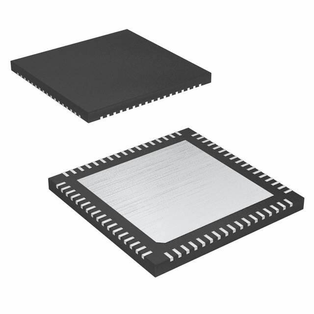


 工商网监
湘ICP备2023018690号
工商网监
湘ICP备2023018690号
