June 16, 2010
Rev 1.0
National Semiconductor
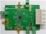
ADC16DV160HFEB
Evaluation Board User’s Guide
ADC16DV160 Dual 16-Bit, 160 MSPS A/D Converter
© 2009 National Semiconductor Corporation.
1
http://www.national.com
�Table of Contents
1.0 Introduction ......................................................................................................................................... 3
2.0 Board Assembly................................................................................................................................... 3
3.0 Quick Start ........................................................................................................................................... 4
4.0 Functional Description......................................................................................................................... 4
4.1 Analog Input .......................................................................................................................... 4
4.2 ADC reference circuitry ........................................................................................................ 4
4.3 ADC clock circuit .................................................................................................................. 5
4.4 Power Supply Connections .................................................................................................... 5
5.0 Installing the ADC16DV160 Evaluation Board .................................................................................. 5
6.0 Hardware Schematic ............................................................................................................................ 6
7.0 Evaluation Board Layout ..................................................................................................................... 7
8.0 Evaluation Board Bill of Materials ...................................................................................................... 10
2
http://www.national.com
�the form of SNR, SINAD, THD SFDR and ENOB. The
latest WaveVision software is available through the
National Semiconductor website:
http://www.national.com/analog/adc/wavevision5
1.0 Introduction
This Evaluation Board may be used to evaluate the
ADC16DV160. The ADC is a dual 16 bit analog to digital
converters that provides data at rates of up to 160 MHz.
2.0 Board Assembly
The evaluation board is designed to be used with the
WaveVision5™ Data Capture Board which is connected
to a personal computer through a USB port and running
WaveVision5™ software, operating under Microsoft
Windows. The software can perform an FFT on the
captured data upon command and, in addition to a
frequency domain plot, shows dynamic performance in
U2
ADC16DV160
The ADC16DV160 Evaluation Board comes preassembled. Refer to the Bill of Materials in Section 8 for
a description of components, to Figure 1 for major
component placement and to Section 6 for the
Evaluation Board schematic.
J2
Input I
P3
1.8V
Wavevision
Connector
P2
1.8V
J4
Clock
Input
J3
Input Q
P1
3.0V
P4
3.0V
Figure 1. Major Component Locations
3
http://www.national.com
�Figure 2: Test Set Up
3.0 Quick Start
Refer to Figure 1 for locations of jumpers, test points and
major components. Refer to Figure 2 for the test set up.
4.
The latest WaveVision software is available through the
National Semiconductor website:
http://www.national.com/analog/adc/wavevision5.
If a software CD is included with the evaluation board kit,
then use the provided software and instructions to install
WaveVision and ensure compatibility with this evaluation
board.
1.
2.
3.
5.
Apply power to the WaveVision5™ board and
connect it to the computer using a USB cable. See
the WaveVision5™ User Guide for operation of that
board. Connect the evaluation board to the
WaveVision5™ Data Capture Board. NOTE: power
to the WaveVision5 Data Capture Board should
be applied before power to the ADC16DV160
Evaluation Board to insure that the FPGA on the
WaveVision5 Data Capture Board is not
damaged.
Connect a clean +3.0V power supply to Power
Connectors P1 and P4. Connect a clean +1.8V
power supply to Power Connectors P2 and P3.
Connect a 160 MHz signal from a 50-Ohm source to
connector J4 for the input Clock. Be sure to use a
bandpass filter before the Evaluation Board. Set the
amplitude to 18 dBm.
Connect a signal from
a 50-Ohm source to
connector J2 (I Channel) or J3 (Q-Channel). Be sure
to use a bandpass filter before the Evaluation Board.
For best results, also attach a 3dB 50 ohm
attenuator right at the input SMA of the eval board.
This will help match the impedance between the
cables/signal source to the eval board input.
Adjust the input signal amplitude as needed to
ensure that the signal does not over-range by
examinining a histogram of the output data with the
WaveVision™ software.
4.0 Functional Description
The ADC16DV160 Evaluation Board schematic is shown
in Section 6. A list of test points and jumper settings can
be found in the Appendix.
4.1 Analog Input
To obtain the best distortion results the analog input
network must be optimized for the signal frequency being
applied. The ADC16DV160 Evaluation Board comes
configured for input frequencies greater than 70MHz. To
accurately evaluate the dynamic performance of this
converter, the input test signal will have to be passed
through a high-quality bandpass filter.
4.2 ADC reference circuitry
4
http://www.national.com
�This Evaluation Board is configured to use the internal
reference.
4.3 ADC clock circuit
Care must be taken to provide a high quality low jitter
clock source. The board is configured to accept a single
ended sinusoidal. It converts the sine wave to a
differential signal through transformer T4. Refer to the
schematic for more detail.
4.4 Power Supply Connections
Power is applied to the board through power connectors
P1 – P4. Care must be taken to observe the correct
polarity.
5.0 Installing the ADC16DV160 Evaluation Board
The evaluation board requires a dual power supplies as
described in Section 4.4. NOTE: power to the
WaveVision5 Data Capture Board should be applied
before power to the ADC16DV160 Evaluation Board
to insure that the FPGA on the WaveVision5 Data
Capture Board is not damaged. A low noise sinusoidal
signal source should be connected to the Clock Input
SMA connector J4. An appropriate signal source should
be connected to the Signal Input SMA connector J2.
When evaluating dynamic performance, an appropriate
signal generator (such as R&S SMA-100A) with 50 Ohm
source impedance should be connected to the Analog
Input connector through an appropriate bandpass filter as
even the best signal generator available can not produce
a signal pure enough to evaluate the dynamic
performance of an ADC.
If this board is used in conjunction with the the
WaveVision5™ Data Capture Board and WaveVision5™
software, a USB cable must be connected between the
Data Capture Board and the host. See the
WaveVision5™ Data Capture Board manual for details.
5
http://www.national.com
�6.0 Hardware Schematic
1
VAD3.0
1
1
SDA
SCL
VCC
VDR1.8
C3
0.1u
2
2
2
R21
10
1
2
24
23
22
21
20
19
18
17
16
15
14
13
12
11
10
9
8
7
6
5
4
3
2
1
1
1
+
VRNI
VA3.0
VRPI
1
2
1
1
1
1
1
C87
22p 0.1u
1
2
1
1
C97
1
2
7
8
R25
2
1
R43
R33
1
1
OUTCLK
JP2
C26
0.01u
VAD3.0
RN3
2
3
4
8
RN_753-08
2
1
1
2
2
24
23
22
21
20
19
18
17
16
15
14
13
12
11
10
9
8
7
6
5
4
3
2
1
0.1u
GND2
C29
VBB
GND2
EN34
RIN8RIN8+
RIN7+
RIN7RIN6RIN6+
R1N5+
RIN5EN
VCC1
RIN4RIN4+
RIN3+
RIN3RIN2RIN2+
RIN1+
RIN1EN12
GND1
GND
0.01u
3
4
5
6
7
CLKCLK+
0
8
RN_753-08
1
2
2
1
2
R12
D0/1
JP3
CSB
SDIO
VA3.0
C51
0.1u
+
GND_TP2 GND_TP3
1
1
1
1
1
C55
0.1u
+
GND2_TP1
1
C54
10uF
1
2
1
GND_4
1
VAD3.0
2
1
P4
C61
0.1u
+
C60
10uF
1
GND_TP4
GND2_TP2
1
2
3
4
5
6
7
8
9
10
11
12
C80
1
VCCA VCCB1
DIR VCCB2
A1
OE
A2
B1
A3
B2
A4
B3
A5
B4
A6
B5
A7
B6
A8
B7
GND1
B8
GND2 GND3
24
23
22
21
20
19
18
17
16
15
14
13
2
VAD3.0
GND2
http://www.national.com
GND2
VCCA VCCB1
DIR
VCCB2
A1
OE
A2
B1
A3
B2
A4
B3
A5
B4
A6
B5
A7
B6
A8
B7
GND1
B8
GND2 GND3
24
23
22
21
20
19
18
17
16
15
14
13
DIR
GND2
SCLK
Connector Future Bus Header96
GND2
+3.3V
GND2
GND2
0.1u
SDIO
National Semiconductor
Title
ADC16DV160HFEB Evaluation Board
2
2
1
1
2
GND_3
1
VDR1.8
VAD3.0
2
P3
1
GND_TP1
1
VA1.8
VDR1.8
6
U7
1
2
3
4
5
6
7
8
9
10
11
12
C77
0.1u
A24
B24
C24
D24
A23
B23
C23
D23
A22
B22
C22
D22
A21
B21
C21
D21
A20
B20
C20
D20
A19
B19
C19
D19
A18
B18
C18
D18
A17
B17
C17
D17
A16
B16
C16
D16
A15
B15
C15
D15
A14
B14
C14
D14
A13
B13
C13
D13
A12
B12
C12
D12
A11
B11
C11
D11
A10
B10
C10
D10
A9
B9
C9
D9
A8
B8
C8
D8
A7
B7
C7
D7
A6
B6
C6
D6
A5
B5
C5
D5
A4
B4
C4
D4
A3
B3
C3
D3
A2
B2
C2
D2
A1
B1
C1
D1
SN74AVC8T245
VAD3.0
U8
1
0.1u
1
C50
10uF
C81
2
1
1
1
2
1
VA3.0
GND_2
VDR1.8
1
2
C48
10uF
VA1.8
C49
0.1u
+
2
2
2
GND_1
P2
1
1
VA3.0
SCLK
VA1.8
2
P1
VDR
SDIO
1
2
1
R31
100
1
TestPoint
D0/1-Q
D0/1+Q
C76
2
1
C37
0.1u
C35
33p
1TP1
1
1
D2/3-Q
D2/3+Q
2
0.1u
6
ADT1_1WT
2
2 1
0.1u
D6/7-Q
D6/7+Q
D4/5-Q
D4/5+Q
1
2
0
C32
1
D8/9-Q
D8/9+Q
2
1
D10/11-Q
D10/11+Q
VDR1.8
RN4
2
4
5
2
D12/13-Q
D12/13+Q
CSB
1
3
25
26
27
28
29
30
31
32
33
34
35
36
37
38
39
40
41
42
43
44
45
46
47
48
VAD3.0
2
R14
VCC2
VCC3
EN56
DOUT8DOUT8+
DOUT7+
DOUT7DOUT6DOUT6+
DOUT5+
DOUT5GND3
GND4
DOUT4DOUT4+
DOUT3+
DOUT3DOUT2DOUT2+
DOUT1+
DOUT1EN78
VCC4
VCC5
FIN1108MTD
VA3.0
T4
OUTCLK+
OUTCLK-
U5
2
C67
7
0.1u
D12/13-I
D12/13+I
D14/15-Q
D14/15+Q
8
7
6
5
FIN1101K8X
6
C27
D10/11-I
D10/11+I
VAD3.0
100
2
5
C31
D8/9-I
D8/9+I
GND2
0
0.1u
D0/1-I
D0/1+I
D2/3-I
D2/3+I
D4/5-I
D4/5+I
D6/7-I
D6/7+I
FIN1108MTD
U6
1
RIN+
2 RINVCC
3 GND
DOUT+
4 EN
GND1 DOUT-
0
2
25
26
27
28
29
30
31
32
33
34
35
36
37
38
39
40
41
42
43
44
45
46
47
48
D14/15-I
D14/15+I
0.1u
2
1
VCC2
VCC3
EN56
DOUT8DOUT8+
DOUT7+
DOUT7DOUT6DOUT6+
DOUT5+
DOUT5GND3
GND4
DOUT4DOUT4+
DOUT3+
DOUT3DOUT2DOUT2+
DOUT1+
DOUT1EN78
VCC4
VCC5
RN_753-08
2
1
2
R42
C28
0.1u
2
6
1
1
1
2
C85
0.1u
C53
10p
24.9
1
C25
0.1u
2
R18
4
5
2
DNP
2
VBB
GND2
EN34
RIN8RIN8+
RIN7+
RIN7RIN6RIN6+
R1N5+
RIN5EN
VCC1
RIN4RIN4+
RIN3+
RIN3RIN2RIN2+
RIN1+
RIN1EN12
GND1
GND
1
2
2
C33
RN2
3
1
2
2
2
2
2
BALANCED_PORT_1
R44
51
50
49
48
47
46
45
44
43
42
41
40
39
38
37
36
35
VA1.8
1
6
1
2
18
19
20
21
22
23
24
25
26
27
28
29
30
31
32
33
34
R13
24.9
7
C56
0.1u
J4
CLK_DIFF
5
4
1
3
1
1
C52
10p
0
1
2
1
1
5
8
DC_BIAS/NC
T2
BD0205F5050A00
ADC16DV160
2
1
1
0
R41
C96
DNP
GND5
4
NC
10
1
R22
10
BALANCED_PORT_2
UNBALANCED
R9
1
U2
0
0.1u
GND9
1
2
9
DNP
2
GND4
2
GND/DIFF_IN
GND10
1
1 2
2
1
INPUT_Q
J3
1
2
C58
0.1u
2
R40
DNP
L2
1
2
2
1 1
3
2
1
1 2
2
1
5
4
3
R39
DNP
VRNQ
1u
C93
R20
49.9
DNP
VRPQ
C16
0.01u
D10/11-I
D10/11+I
D12/13-I
D12/13+I
D14/15-I
D14/15+I
OUTCLKOUTCLK+
D14/15-Q
D14/15+Q
D12/13-Q
D12/13+Q
D10/11-Q
D10/11+Q
D8/9-Q
D8/9+Q
D6/7-Q
AGND_18
VIN-Q
VIN+Q
AGND_21
VA3.0_22
SCLK
SDI
CLKCLK+
CSB
D0/1+Q
D0/1-Q
D2/3+Q
D2/3-Q
D4/5+Q
D4/5-Q
D6/7+Q
C83
0.1u
C15
0.1u
2
C79
2
2
+
1
VA1.8_1
VRMI
AGND_3
VA3.0_4
VRNI
VRNI_6
VRPI
VRPI_8
VREF
VRPQ
VRPQ_11
VRNQ
VRNQ_13
VA3.0_14
AGND
VRMQ
VA1.8_17
D14/15
JP1
GND69
GND70
C78
10uF
C95
DNP
8
68
67
66
65
64
63
62
61
60
59
58
57
56
55
54
53
52
2
2
2
2
C74
0.1u
2
C94
DNP
1
2
3
4
5
6
7
8
9
10
11
12
13
14
15
16
17
1
1
1
1
2
C75
0.1u
C47
0.1u
6
69
70
C59
0.1u
10uF
C65
0.1u
4
5
7
68_AGND
VIN-I
VIN+I
65_AGND
64_VA3.0
DRGND
VDR1.8
D0/1-I
DO/1+I
D2/3-I
D2/3+I
D4/5-I
D4/5+I
D6/7-I
D6/7+I
D8/9-I
D8/9+I
2
10uF
2
1TP5
+
1
C66
0.1u
1
1
VA3.0
1
C72
2
2
3
2
0.1u
+
1
1
1
C64
TP41
2
1TP3
C8
0.01u
RN1
RN_753-08
1
1
1
C84
0.1u
2
2
C14
0.01u
C6
0.1u
2
C71
C12
0.1u
C86
0.1u
2
0.1u
0.1u
1u
2
C63
1
0.1u
2
1
0.1u
1
1
TP21
C82
C73
2
1
1
1
1
2
1
C62
2
2
VRNQ
1
C34
VRPQ
J1
A24
B24
C24
D24
A23
B23
C23
D23
A22
B22
C22
D22
A21
B21
C21
D21
A20
B20
C20
D20
A19
B19
C19
D19
A18
B18
C18
D18
A17
B17
C17
D17
A16
B16
C16
D16
A15
B15
C15
D15
A14
B14
C14
D14
A13
B13
C13
D13
A12
B12
C12
D12
A11
B11
C11
D11
A10
B10
C10
D10
A9
B9
C9
D9
A8
B8
C8
D8
A7
B7
C7
D7
A6
B6
C6
D6
A5
B5
C5
D5
A4
B4
C4
D4
A3
B3
C3
D3
A2
B2
C2
D2
A1
B1
C1
D1
U4
C4
0.01u
R38
0
VA1.8
VRNI
+5V
GND2
C70
0.01u
2
C69
0.1u
2
2
2
C68
0.01u
GND2
R10
0
VRPI
GND
2
1
1
2
2
1
2
C46
0.1u
VAD3.0
1
1
1
1
1
1
2
2
1
1
2
2
0.01u
1
1
2
10uF
1
5
2
2
2
2
GND5
5
4
C92
C38
2
C43
0.1u
C13
10p
24.9
0.1u
C41
C2
0.01u
2
1
R7
1
WP
24C02-SO8
1
1
VA3.0
C1
0.1u
DNP
C24
0.1u
SCL
7
VAD3.0
C21
22p
R45
SDA
4
1
6
BALANCED_PORT_1
A0
A1
A2
2
R35
0
2
C23
0.01u
2
2
2
1
1
C30
0.1u
VCC
U3
1
2
3
C40
6
C7
10p
R5
24.9
0.1u
0.01u
C36
GND2
7
DC_BIAS/NC
GND/DIFF_IN
2
C91
DNP
1
1
C90
DNP
GND9
NC
3
C89
DNP
GND4
R37
DNP
1
R36
DNP
8
BALANCED_PORT_2
21
R6
49.9
DNP
UNBALANCED
2
0.1u
C20
2
1
0.1u
1
2
1
DNP
21
2
2
L1
2
0.1u
2
1
1
GND10
C17
1
2
J2
INPUT_I
5
4
3
R3
1
0.1u
2
2
2
1
1
1
1
0.01u
C19
0
10
1
9
R34
0
2
0.1u
C88
2
T1
BD0205F5050A00
C11
8
C9
0.1u
C10
SN74AVC8T245
GND2
Size
C
Document Number
Date:
Wednesday, May 19, 2010
Rev
1
Sheet
1
of
1
�7.0 Evaluation Board Layout
Layer 1: Component Side
Layer 2: Ground
7
http://www.national.com
�Layer 3: Power
Layer 4: Ground, Clock
8
http://www.national.com
�Layer 5: Ground
Layer 6: Circuit Side
9
http://www.national.com
�8.0 Evaluation Board Bill of Materials
Item Quantity
Reference
______________________________________________
1
11
2
13
3
4
4
12
5
30
6
7
8
9
10
13
2
1
4
4
2
6
17
18
19
20
22
23
24
25
26
27
1
1
1
1
1
1
1
1
4
10
28
30
31
32
37
38
39
40
41
42
43
4
2
2
2
2
1
1
1
2
1
2
NSC
NSC
NSC
C1,C3,C6,C12,C15,C25,C27,
C34,C79,C86,C87
C2,C4,C8,C11,C14,C16,C20,
C26,C29,C40,C43,C68,C70
C7,C13,C52,C53
C9,C17,C23,C28,C31,C32,
C37,C49,C51,C55,C58,C61
C10,C19,C24,C30,C36,C41,
C46,C47,C56,C59,C62,C63,
C65,C66,C67,C69,C71,C73,
C74,C75,C76,C77,C80,C81,
C84,C85,C88,C92,C93,C97
C21,C33
C35
C38,C64,C72,C78
C48,C50,C54,C60
C82,C83
GND_TP1,GND_TP2,GND_TP3,
GND_TP4,GND2_TP1,
GND2_TP2
J1
J2
J3
J4
P1
P2
P3
P4
RN1,RN2,RN3,RN4
R3,R9,R10,R25,R34,R35,
R38,R41,R42,R43
R5,R7,R13,R18
R12,R14
R21,R22
R31,R33
T1,T2
T4
U2
U3
U4,U5
U6
U7,U8
Part
Manufacturer
Manufacturer P/N
0.1u
Murata
GRM033R60J104KE19D
0.01u
Murata
GRM155R71H103KA88D
10p
0.1u
Murata
Murata
GRM1555C1H100JZ01D
GRM188R71C104KA01D
0.1u
Murata
GRM155R61A104KA01D
22p
33p
10uF
10uF
1u
TestPoint
Murata
Murata
Nichicon
AVX
Panasonic
Keystone
GRM1555C1H220JZ01D
GRM1555C1H330JZ01D
F931A106MAA
TAJC106K020R
ECY-29RA105KV
5002
Connector Future Bus Header96
INPUT_I
INPUT_Q
CLK_DIFF
VA3.0
VA1.8
VDR
VAD3.0
RN_753-08
0
Tyco Electronics
Johnson
Johnson
Johnson
Phoenix Contacts
Phoenix Contacts
Phoenix Contacts
Phoenix Contacts
CTS Resistor
Yageo
5223514-3
142-0701-851
142-0701-851
142-0701-851
1759017
1759017
1759017
1759017
753083101GTR
RC0402JR-070RL
24.9
0
10
100
BD0205F5050A00
ADT1_1WT
ADC16DV160
24C02-SO8
FIN1108MTD
FIN1101K8X
SN74AVC8T245
Panasonic - ECG
Yageo
Panasonic - ECG
Panasonic - ECG
Anaren
Mini-Circuits
National Semiconductor
Atmel
Fairchild
Fairchild
Texas Instuments
ERJ-2RKF24R9X
RC0603JR-070RL
ERJ-3EKF10R0V
ERJ-2RKF1000X
BD0205F5050A00
ADT1-1WT+
ADC16DV160
AT24HC02BN-SH-B
FIN1108MTD
FIN1101K8X
SN74AVC8T245DGVR
10
http://www.national.com
�BY USING THIS PRODUCT, YOU ARE AGREEING TO BE BOUND BY THE TERMS AND CONDITIONS OF NATIONAL
SEMICONDUCTOR'S END USER LICENSE AGREEMENT. DO NOT USE THIS PRODUCT UNTIL YOU HAVE READ AND AGREED
TO THE TERMS AND CONDITIONS OF THAT AGREEMENT. IF YOU DO NOT AGREE WITH THEM, CONTACT THE VENDOR
WITHIN TEN (10) DAYS OF RECEIPT FOR INSTRUCTIONS ON RETURN OF THE UNUSED PRODUCT FOR A REFUND OF THE
PURCHASE PRICE PAID, IF ANY.
The ADC16DV160 Evaluation Boards are intended for product evaluation purposes only and are not intended for resale to end
consumers, is not authorized for such use and is not designed for compliance with European EMC Directive 89/336/EEC, or for
compliance with any other electromagnetic compatibility requirements.
National Semiconductor Corporation does not assume any responsibility for use of any circuitry or software supplied or described. No
circuit patent licenses are implied.
LIFE SUPPORT POLICY
NATIONAL'S PRODUCTS ARE NOT AUTHORIZED FOR USE AS CRITICAL COMPONENTS IN LIFE SUPPORT DEVICES OR
SYSTEMS WITHOUT THE EXPRESS WRITTEN APPROVAL OF THE PRESIDENT OF NATIONAL SEMICONDUCTOR
CORPORATION. As used herein:
1. Life support devices or systems are devices or systems
which, (a) are intended for surgical implant into the body,
or (b) support or sustain life, and whose failure to perform,
when properly used in accordance with instructions for use
provided in the labeling, can be reasonably expected to
result in a significant injury to the user.
National Semiconductor Corporation
Americas
Tel:
1-800-272-9959
Fax: 1-800-737-7018
Email: support@nsc.com
2. A critical component is any component in a life support
device or system whose failure to perform can be
reasonably expected to cause the failure of the life support
device or system, or to affect its safety or effectiveness.
National Semiconductor Europe
Fax: +49 (0) 1 80-530 85 86
Email: europe.support@nsc.com
Deutsch Tel: +49 (0) 699508 6208
English Tel: +49 (0) 870 24 0 2171
Français Tel: +49 (0) 141 91 8790
National Semiconductor
Asia Pacific Customer
Response Group
Tel: 65-2544466
Fax: 65-2504466
Email:sea.support@nsc.com
National Semiconductor
Japan Ltd.
Tel: 81-3-5639-7560
Fax: 81-3-5639-7507
www.national.com
National does not assume any responsibility for any circuitry described, no circuit patent licenses are implied and National reserves the right at any time
without notice to change said circuitry and specifications.
11
http://www.national.com
�IMPORTANT NOTICE
Texas Instruments Incorporated and its subsidiaries (TI) reserve the right to make corrections, modifications, enhancements, improvements,
and other changes to its products and services at any time and to discontinue any product or service without notice. Customers should
obtain the latest relevant information before placing orders and should verify that such information is current and complete. All products are
sold subject to TI’s terms and conditions of sale supplied at the time of order acknowledgment.
TI warrants performance of its hardware products to the specifications applicable at the time of sale in accordance with TI’s standard
warranty. Testing and other quality control techniques are used to the extent TI deems necessary to support this warranty. Except where
mandated by government requirements, testing of all parameters of each product is not necessarily performed.
TI assumes no liability for applications assistance or customer product design. Customers are responsible for their products and
applications using TI components. To minimize the risks associated with customer products and applications, customers should provide
adequate design and operating safeguards.
TI does not warrant or represent that any license, either express or implied, is granted under any TI patent right, copyright, mask work right,
or other TI intellectual property right relating to any combination, machine, or process in which TI products or services are used. Information
published by TI regarding third-party products or services does not constitute a license from TI to use such products or services or a
warranty or endorsement thereof. Use of such information may require a license from a third party under the patents or other intellectual
property of the third party, or a license from TI under the patents or other intellectual property of TI.
Reproduction of TI information in TI data books or data sheets is permissible only if reproduction is without alteration and is accompanied
by all associated warranties, conditions, limitations, and notices. Reproduction of this information with alteration is an unfair and deceptive
business practice. TI is not responsible or liable for such altered documentation. Information of third parties may be subject to additional
restrictions.
Resale of TI products or services with statements different from or beyond the parameters stated by TI for that product or service voids all
express and any implied warranties for the associated TI product or service and is an unfair and deceptive business practice. TI is not
responsible or liable for any such statements.
TI products are not authorized for use in safety-critical applications (such as life support) where a failure of the TI product would reasonably
be expected to cause severe personal injury or death, unless officers of the parties have executed an agreement specifically governing
such use. Buyers represent that they have all necessary expertise in the safety and regulatory ramifications of their applications, and
acknowledge and agree that they are solely responsible for all legal, regulatory and safety-related requirements concerning their products
and any use of TI products in such safety-critical applications, notwithstanding any applications-related information or support that may be
provided by TI. Further, Buyers must fully indemnify TI and its representatives against any damages arising out of the use of TI products in
such safety-critical applications.
TI products are neither designed nor intended for use in military/aerospace applications or environments unless the TI products are
specifically designated by TI as military-grade or "enhanced plastic." Only products designated by TI as military-grade meet military
specifications. Buyers acknowledge and agree that any such use of TI products which TI has not designated as military-grade is solely at
the Buyer's risk, and that they are solely responsible for compliance with all legal and regulatory requirements in connection with such use.
TI products are neither designed nor intended for use in automotive applications or environments unless the specific TI products are
designated by TI as compliant with ISO/TS 16949 requirements. Buyers acknowledge and agree that, if they use any non-designated
products in automotive applications, TI will not be responsible for any failure to meet such requirements.
Following are URLs where you can obtain information on other Texas Instruments products and application solutions:
Products
Applications
Audio
www.ti.com/audio
Automotive and Transportation www.ti.com/automotive
Amplifiers
amplifier.ti.com
Communications and Telecom www.ti.com/communications
Data Converters
dataconverter.ti.com
Computers and Peripherals
www.ti.com/computers
DLP® Products
www.dlp.com
Consumer Electronics
www.ti.com/consumer-apps
DSP
dsp.ti.com
Energy and Lighting
www.ti.com/energy
Clocks and Timers
www.ti.com/clocks
Industrial
www.ti.com/industrial
Interface
interface.ti.com
Medical
www.ti.com/medical
Logic
logic.ti.com
Security
www.ti.com/security
Power Mgmt
power.ti.com
Space, Avionics and Defense
www.ti.com/space-avionics-defense
Microcontrollers
microcontroller.ti.com
Video and Imaging
www.ti.com/video
RFID
www.ti-rfid.com
OMAP Mobile Processors
www.ti.com/omap
Wireless Connectivity
www.ti.com/wirelessconnectivity
TI E2E Community Home Page
e2e.ti.com
Mailing Address: Texas Instruments, Post Office Box 655303, Dallas, Texas 75265
Copyright © 2012, Texas Instruments Incorporated
�


 工商网监
湘ICP备2023018690号
工商网监
湘ICP备2023018690号
