Sample &
Buy
Product
Folder
Support &
Community
Tools &
Software
Technical
Documents
ADC3441, ADC3442, ADC3443, ADC3444
SBAS670A – JULY 2014 – REVISED OCTOBER 2015
ADC344x Quad-Channel, 14-Bit, 25-MSPS to 125-MSPS, Analog-to-Digital Converter
1 Features
3 Description
•
•
•
•
•
•
The ADC344x are a high-linearity, ultra-low power,
quad-channel, 14-bit, 25-MSPS to 125-MSPS,
analog-to-digital converter (ADC) family. The devices
are designed specifically to support demanding, high
input frequency signals with large dynamic range
requirements. An input clock divider allows more
flexibility for system clock architecture design while
the SYSREF input enables complete system
synchronization. The ADC344x family supports serial
low-voltage differential signaling (LVDS) in order to
reduce the number of interface lines, thus allowing for
high system integration density. The serial LVDS
interface is two-wire, where each ADC data are
serialized and output over two LVDS pairs. An
internal phase-locked loop (PLL) multiplies the
incoming ADC sampling clock to derive the bit clock
that is used to serialize the 14-bit output data from
each channel. In addition to the serial data streams,
the frame and bit clocks are also transmitted as
LVDS outputs.
1
•
•
•
•
•
•
Quad Channel
14-Bit Resolution
Single Supply: 1.8 V
Serial LVDS Interface
Flexible Input Clock Buffer with Divide-by-1, -2, -4
SNR = 72.4 dBFS, SFDR = 87 dBc at
fIN = 70 MHz
Ultra-Low Power Consumption:
– 98 mW/Ch at 125 MSPS
Channel Isolation: 105 dB
Internal Dither and Chopper
Support for Multi-Chip Synchronization
Pin-to-Pin Compatible with 12-Bit Version
Package: VQFN-56 (8 mm × 8 mm)
2 Applications
•
•
•
•
•
•
•
•
•
•
Multi-Carrier, Multi-Mode Cellular Base Stations
Radar and Smart Antenna Arrays
Munitions Guidance
Motor Control Feedback
Network and Vector Analyzers
Communications Test Equipment
Nondestructive Testing
Microwave Receivers
Software-Defined Radios (SDRs)
Quadrature and Diversity Radio Receivers
Device Information(1)
PART NUMBER
ADC344x
PACKAGE
VQFN (56)
BODY SIZE (NOM)
8.00 mm × 8.00 mm
(1) For all available packages, see the orderable addendum at
the end of the datasheet.
space
space
space
space
space
space
Spectrum at 10-MHz IF
(SFDR = 95 dBc, SNR = 72.7 dBFS, SINAD = 72.6 dBFS,
THD = 100 dBc, HD2 = 95 dBc, HD3 = 96 dBc)
0
-10
-20
Amplitude (dBFS)
-30
-40
-50
-60
-70
-80
-90
-100
-110
-120
0
12.5
25
37.5
Frequency (MHz)
50
62.5
D101
1
An IMPORTANT NOTICE at the end of this data sheet addresses availability, warranty, changes, use in safety-critical applications,
intellectual property matters and other important disclaimers. PRODUCTION DATA.
�ADC3441, ADC3442, ADC3443, ADC3444
SBAS670A – JULY 2014 – REVISED OCTOBER 2015
www.ti.com
Table of Contents
1
2
3
4
5
6
7
Features ..................................................................
Applications ...........................................................
Description .............................................................
Revision History.....................................................
Device Comparison Table.....................................
Pin Configuration and Functions .........................
Specifications.........................................................
7.1
7.2
7.3
7.4
7.5
7.6
7.7
7.8
7.9
7.10
7.11
7.12
7.13
7.14
7.15
7.16
7.17
7.18
1
1
1
2
3
3
5
Absolute Maximum Ratings ...................................... 5
ESD Ratings.............................................................. 5
Recommended Operating Conditions....................... 5
Thermal Information .................................................. 6
Electrical Characteristics: General ............................ 6
Electrical Characteristics: ADC3441, ADC3442 ....... 7
Electrical Characteristics: ADC3443, ADC3444 ....... 7
AC Performance: ADC3441...................................... 8
AC Performance: ADC3442.................................... 10
AC Performance: ADC3443.................................. 12
AC Performance: ADC3444.................................. 14
Digital Characteristics ........................................... 16
Timing Requirements: General ............................. 16
Timing Requirements: LVDS Output..................... 17
Typical Characteristics: ADC3441 ........................ 18
Typical Characteristics: ADC3442 ........................ 24
Typical Characteristics: ADC3443 ........................ 30
Typical Characteristics: ADC3444 ........................ 36
7.19 Typical Characteristics: Common ......................... 42
7.20 Typical Characteristics: Contour ........................... 43
8
Parameter Measurement Information ................ 43
9
Detailed Description ............................................ 45
8.1 Timing Diagrams ..................................................... 43
9.1
9.2
9.3
9.4
9.5
9.6
Overview .................................................................
Functional Block Diagram .......................................
Feature Description.................................................
Device Functional Modes........................................
Programming...........................................................
Register Maps .........................................................
45
45
46
50
51
55
10 Applications and Implementation...................... 70
10.1 Application Information.......................................... 70
10.2 Typical Applications .............................................. 71
11 Power Supply Recommendations ..................... 73
12 Layout................................................................... 74
12.1 Layout Guidelines ................................................. 74
12.2 Layout Example .................................................... 74
13 Device and Documentation Support ................. 75
13.1
13.2
13.3
13.4
13.5
Related Links ........................................................
Community Resources..........................................
Trademarks ...........................................................
Electrostatic Discharge Caution ............................
Glossary ................................................................
75
75
75
75
75
14 Mechanical, Packaging, and Orderable
Information ........................................................... 75
4 Revision History
NOTE: Page numbers for previous revisions may differ from page numbers in the current version.
Changes from Original (July 2014) to Revision A
•
2
Page
Released to production........................................................................................................................................................... 1
Submit Documentation Feedback
Copyright © 2014–2015, Texas Instruments Incorporated
Product Folder Links: ADC3441 ADC3442 ADC3443 ADC3444
�ADC3441, ADC3442, ADC3443, ADC3444
www.ti.com
SBAS670A – JULY 2014 – REVISED OCTOBER 2015
5 Device Comparison Table
INTERFACE
Serial LVDS
JESD204B
RESOLUTION
(Bits)
25 MSPS
50 MSPS
80 MSPS
125 MSPS
160 MSPS
12
ADC3421
ADC3422
ADC3423
ADC3424
—
14
ADC3441
ADC3442
ADC3443
ADC3444
—
12
—
ADC34J22
ADC34J23
ADC34J24
ADC34J25
14
—
ADC34J42
ADC34J43
ADC34J44
ADC34J45
6 Pin Configuration and Functions
DB0M
DB0P
DB1M
DB1P
DVDD
DCLKM
DCLKP
FCLKM
FCLKP
DVDD
DC0M
DC0P
DC1M
DC1P
RTQ Package
VQFN-56
Top View
56
55
54
53
52
51
50
49
48
47
46
45
44
43
DA0M
4
39
DD1P
DVDD
5
38
DVDD
AVDD
6
37
PDN
AVDD
7
GND Pad
36
AVDD
INAM
8
(Back Side)
35
INDM
INAP
9
34
INDP
AVDD
10
33
AVDD
AVDD
11
32
AVDD
INBP
12
31
INCP
INBM
13
30
INCM
AVDD
14
29
AVDD
17
18
19
20
21
Copyright © 2014–2015, Texas Instruments Incorporated
22
23
24
25
26
27
28
AVDD
16
CLKP
15
VCM
DD1M
SYSREFM
40
SYSREFP
3
RESET
DA0P
AVDD
DD0P
CLKM
41
AVDD
2
SDOUT
DA1M
SEN
DD0M
SDATA
42
SCLK
1
AVDD
DA1P
Submit Documentation Feedback
Product Folder Links: ADC3441 ADC3442 ADC3443 ADC3444
3
�ADC3441, ADC3442, ADC3443, ADC3444
SBAS670A – JULY 2014 – REVISED OCTOBER 2015
www.ti.com
Pin Functions
PIN
NAME
I/O
NO.
DESCRIPTION
AVDD
6, 7, 10, 11, 14,
15, 20, 23, 28, 29,
32, 33, 36
I
Analog 1.8-V power supply
CLKM
21
I
Negative differential clock input for the ADC
CLKP
22
I
Positive differential clock input for the ADC
DA0M
4
O
Negative serial LVDS output for wire-0 of channel A
DA0P
3
O
Positive serial LVDS output for wire-0 of channel A
DA1M
2
O
Negative serial LVDS output for wire-1 of channel A
DA1P
1
O
Positive serial LVDS output for wire-1 of channel A
DB0M
56
O
Negative serial LVDS output for wire-0 of channel B
DB0P
55
O
Positive serial LVDS output for wire-0 of channel B
DB1M
54
O
Negative serial LVDS output for wire-1 of channel B
DB1P
53
O
Positive serial LVDS output for wire-1 of channel B1
DC0M
46
O
Negative serial LVDS output for wire-0 of channel C
DC0P
45
O
Positive serial LVDS output for wire-0 of channel C
DC1M
44
O
Negative serial LVDS output for wire-1 of channel C
DC1P
43
O
Positive serial LVDS output for wire-1 of channel C
DD0M
42
O
Negative serial LVDS output for wire-0 of channel D
DD0P
41
O
Positive serial LVDS output for wire-0 of channel D
DD1M
40
O
Negative serial LVDS output for wire-1 of channel D
DD1P
39
O
Positive serial LVDS output for wire-1 of channel D
DCLKM
51
O
Negative bit clock output
DCLKP
50
O
Positive bit clock output
DVDD
5, 38, 47, 52
I
Digital 1.8-V power supply
FCLKM
49
O
Negative frame clock output
FCLKP
48
O
Positive frame clock output
GND
PowerPAD™
I
Ground, 0 V
INAM
8
I
Negative differential analog input for channel A
INAP
9
I
Positive differential analog input for channel A
INBM
13
I
Negative differential analog input for channel B
INBP
12
I
Positive differential analog input for channel B
INCM
30
I
Negative differential analog input for channel C
INCP
31
I
Positive differential analog input for channel C
INDM
35
I
Negative differential analog input for channel D
INDP
34
I
Positive differential analog input for channel D
PDN
37
I
Power-down control. This pin can be configured via the SPI.
This pin has an internal 150-kΩ pulldown resistor.
RESET
24
I
Hardware reset; active high. This pin has an internal 150-kΩ pulldown resistor.
SCLK
16
I
Serial interface clock input. This pin has an internal 150-kΩ pulldown resistor.
SDATA
17
I
Serial interface data input. This pin has an internal 150-kΩ pulldown resistor.
SDOUT
19
O
Serial interface data output
SEN
18
I
Serial interface enable; active low.
This pin has an internal 150-kΩ pullup resistor to AVDD.
SYSREFM
26
I
Negative external SYSREF input
SYSREFP
25
I
Positive external SYSREF input
VCM
27
O
Common-mode voltage for analog inputs
4
Submit Documentation Feedback
Copyright © 2014–2015, Texas Instruments Incorporated
Product Folder Links: ADC3441 ADC3442 ADC3443 ADC3444
�ADC3441, ADC3442, ADC3443, ADC3444
www.ti.com
SBAS670A – JULY 2014 – REVISED OCTOBER 2015
7 Specifications
7.1 Absolute Maximum Ratings
over operating free-air temperature range (unless otherwise noted) (1)
MIN
MAX
UNIT
Analog supply voltage range, AVDD
–0.3
2.1
V
Digital supply voltage range, DVDD
V
Voltage applied to
input pins
Temperature
–0.3
2.1
INAP, INBP, INAM, INBM
–0.3
min (1.9, AVDD + 0.3)
CLKP, CLKM
–0.3
AVDD + 0.3
SYSREFP, SYSREFM
–0.3
AVDD + 0.3
SCLK, SEN, SDATA, RESET, PDN
–0.3
3.9
Operating free-air, TA
–40
85
Operating junction, TJ
Storage, Tstg
(1)
V
125
–65
ºC
150
Stresses beyond those listed under Absolute Maximum Ratings may cause permanent damage to the device. These are stress ratings
only, which do not imply functional operation of the device at these or any other conditions beyond those indicated under Recommended
Operating Conditions. Exposure to absolute-maximum-rated conditions for extended periods may affect device reliability.
7.2 ESD Ratings
V(ESD)
(1)
Human body model (HBM), per ANSI/ESDA/JEDEC JS-001 (1)
Electrostatic discharge
VALUE
UNIT
±2000
V
JEDEC document JEP155 states that 500-V HBM allows safe manufacturing with a standard ESD control process.
7.3 Recommended Operating Conditions (1)
over operating free-air temperature range (unless otherwise noted)
MIN
NOM
MAX
UNIT
SUPPLIES
AVDD
Analog supply voltage range
1.7
1.8
1.9
V
DVDD
Digital supply voltage range
1.7
1.8
1.9
V
ANALOG INPUT
VID
Differential input voltage
VIC
Input common-mode voltage
For input frequencies < 450 MHz
2
For input frequencies < 600 MHz
1
VPP
VCM ± 0.025
V
CLOCK INPUT
Input clock frequency
Sampling clock frequency
Sine wave, ac-coupled
Input clock amplitude (differential)
15 (2)
0.2
125 (3)
1.5
LPECL, ac-coupled
1.6
LVDS, ac-coupled
0.7
Input clock duty cycle
35%
Input clock common-mode voltage
MSPS
50%
VPP
65%
0.95
V
DIGITAL OUTPUTS
CLOAD
Maximum external load capacitance from each output pin to GND
3.3
pF
RLOAD
Single-ended load resistance
100
Ω
(1)
(2)
(3)
After power-up, use only the RESET pin to reset the device for the first time; see the Register Initialization section for details.
See Table 3 for details.
With the clock divider enabled by default for divide-by-1. Maximum sampling clock frequency for the divide-by-4 option is 500 MSPS.
Copyright © 2014–2015, Texas Instruments Incorporated
Submit Documentation Feedback
Product Folder Links: ADC3441 ADC3442 ADC3443 ADC3444
5
�ADC3441, ADC3442, ADC3443, ADC3444
SBAS670A – JULY 2014 – REVISED OCTOBER 2015
www.ti.com
7.4 Thermal Information
ADC344x
THERMAL METRIC (1)
RTQ (VQFN)
UNIT
56 PINS
RθJA
Junction-to-ambient thermal resistance
25.3
°C/W
RθJC(top)
Junction-to-case (top) thermal resistance
9.5
°C/W
RθJB
Junction-to-board thermal resistance
3.4
°C/W
ψJT
Junction-to-top characterization parameter
0.2
°C/W
ψJB
Junction-to-board characterization parameter
3.3
°C/W
RθJC(bot)
Junction-to-case (bottom) thermal resistance
0.5
°C/W
(1)
For more information about traditional and new thermal metrics, see the IC Package Thermal Metrics application report, SPRA953.
7.5 Electrical Characteristics: General
Typical values are over the operating free-air temperature range, at TA = 25°C, full temperature range is TMIN = –40°C to TMAX
= 85°C, maximum sampling rate, 50% clock duty cycle, AVDD = DVDD = 1.8 V, and –1-dBFS differential input, unless
otherwise noted.
PARAMETER
TEST CONDITIONS
MIN
TYP
MAX
UNIT
ANALOG INPUT
2.0
VPP
ri
Differential input full-scale
Input resistance
Differential at dc
6.6
kΩ
ci
Input capacitance
Differential at dc
3.7
pF
VOC(VCM)
VCM common-mode voltage
output
0.95
V
VCM output current capability
10
mA
Input common-mode current
Per analog input pin
1.5
µA/MSPS
Analog input bandwidth (3 dB)
50-Ω differential source driving 50-Ω
termination across INP and INM
540
MHz
DC ACCURACY
EO
Offset error
αEO
Temperature coefficient of offset
error
–25
EG(REF)
Gain error as a result of internal
reference inaccuracy alone
EG(CHAN)
Gain error of channel alone
α(EGCHAN)
Temperature coefficient of
EG(CHAN)
25
±0.024
–2
mV/°C
2
–2
±0.008
mV
%FS
%FS
Δ%FS/Ch
CHANNEL-TO-CHANNEL ISOLATION
fIN = 10 MHz
fIN = 100 MHz
Crosstalk (1)
fIN = 200 MHz
fIN = 230 MHz
fIN = 300 MHz
(1)
6
Near channel
105
Far channel
105
Near channel
95
Far channel
105
Near channel
94
Far channel
105
Near channel
dB
92
Far channel
105
Near channel
85
Far channel
105
Crosstalk is measured with a –1-dBFS input signal on the aggressor channel and no input on the victim channel.
Submit Documentation Feedback
Copyright © 2014–2015, Texas Instruments Incorporated
Product Folder Links: ADC3441 ADC3442 ADC3443 ADC3444
�ADC3441, ADC3442, ADC3443, ADC3444
www.ti.com
SBAS670A – JULY 2014 – REVISED OCTOBER 2015
7.6 Electrical Characteristics: ADC3441, ADC3442
Typical values are over the operating free-air temperature range, at TA = 25°C, full temperature range is TMIN = –40°C to TMAX
= 85°C, maximum sampling rate, 50% clock duty cycle, AVDD = DVDD = 1.8 V, and –1-dBFS differential input, unless
otherwise noted.
ADC3441
PARAMETER
MIN
TYP
ADC clock frequency
ADC3442
MAX
MIN
TYP
25
Resolution
14
MAX
UNIT
50
MSPS
14
Bits
1.8-V analog supply current
54
74
71
97
mA
1.8-V digital supply current
45
67
56
83
mA
177
215
228
277
mW
5
17
5
17
mW
34
103
35
103
mW
Total power dissipation
Global power-down dissipation
Standby power-down dissipation
7.7 Electrical Characteristics: ADC3443, ADC3444
Typical values are over the operating free-air temperature range, at TA = 25°C, full temperature range is TMIN = –40°C to TMAX
= 85°C, maximum sampling rate, 50% clock duty cycle, AVDD = DVDD = 1.8 V, and –1-dBFS differential input, unless
otherwise noted.
ADC3443
PARAMETER
MIN
TYP
ADC clock frequency
ADC3444
MAX
MIN
TYP
80
Resolution
14
1.8-V analog supply current
1.8-V digital supply current
Total power dissipation
Global power-down dissipation
Standby power-down dissipation
Copyright © 2014–2015, Texas Instruments Incorporated
MAX
UNIT
125
MSPS
14
92
125
Bits
119
162
mA
68
101
98
145
mA
288
350
391
475
mW
5
17
5
17
mW
40
103
43
103
mW
Submit Documentation Feedback
Product Folder Links: ADC3441 ADC3442 ADC3443 ADC3444
7
�ADC3441, ADC3442, ADC3443, ADC3444
SBAS670A – JULY 2014 – REVISED OCTOBER 2015
www.ti.com
7.8 AC Performance: ADC3441
Typical values are over the operating free-air temperature range, at TA = 25°C, full temperature range is TMIN = –40°C to TMAX
= 85°C, ADC sampling rate = 25 MSPS, 50% clock duty cycle, AVDD = DVDD = 1.8 V, and –1-dBFS differential input, unless
otherwise noted.
ADC3441 (fS = 25 MSPS)
DITHER ON
PARAMETER
TEST CONDITIONS
MIN
fIN = 10 MHz
SNR
Signal-to-noise ratio
(full Nyquist band)
Noise spectral density
(averaged across Nyquist zone)
NSD (1)
73.4
fIN = 70 MHz
72.5
73
fIN = 100 MHz
72.4
72.7
fIN = 170 MHz
71.4
71.7
fIN = 230 MHz
70.3
70.5
fIN = 10 MHz
72.4
72.9
fIN = 20 MHz
72.2
72.7
fIN = 70 MHz
71.9
72.4
fIN = 100 MHz
71.7
72.0
fIN = 170 MHz
70.9
71.1
fIN = 230 MHz
69.7
69.9
fIN = 10 MHz
–143.7
–144.1
fIN = 20 MHz
–143.5 –141.5
–143.9
fIN = 70 MHz
–143.1
–143.6
fIN = 100 MHz
–143.0
–143.3
fIN = 170 MHz
–142.0
–142.3
fIN = 230 MHz
–140.9
–141.1
73.1
73.4
72.9
73.2
fIN = 70 MHz
71.7
71.9
fIN = 100 MHz
72.6
72.8
fIN = 170 MHz
71.2
71.4
fIN = 230 MHz
69.9
70.1
fIN = 10 MHz
11.9
11.9
11.8
11.8
fIN = 70 MHz
11.7
11.8
fIN = 100 MHz
11.8
11.8
fIN = 170 MHz
11.5
11.6
fIN = 230 MHz
11.3
11.4
91
89
91
85
fIN = 70 MHz
92
87
fIN = 100 MHz
85
82
fIN = 170 MHz
86
85
fIN = 230 MHz
81
81
fIN = 20 MHz
ENOB (1)
Effective number of bits
69.9
11.3
fIN = 10 MHz
fIN = 20 MHz
SFDR
(1)
8
Spurious-free dynamic range
TYP
73.5
fIN = 20 MHz
Signal-to-noise and distortion
ratio
MIN
72.9
70.9
fIN = 10 MHz
SINAD (1)
DITHER OFF
MAX
73.1
fIN = 20 MHz
Signal-to-noise ratio
(from 1-MHz offset)
TYP
82
MAX
UNIT
dBFS
dBFS/Hz
dBFS
Bits
dBc
Reported from a 1-MHz offset.
Submit Documentation Feedback
Copyright © 2014–2015, Texas Instruments Incorporated
Product Folder Links: ADC3441 ADC3442 ADC3443 ADC3444
�ADC3441, ADC3442, ADC3443, ADC3444
www.ti.com
SBAS670A – JULY 2014 – REVISED OCTOBER 2015
AC Performance: ADC3441 (continued)
Typical values are over the operating free-air temperature range, at TA = 25°C, full temperature range is TMIN = –40°C to TMAX
= 85°C, ADC sampling rate = 25 MSPS, 50% clock duty cycle, AVDD = DVDD = 1.8 V, and –1-dBFS differential input, unless
otherwise noted.
ADC3441 (fS = 25 MSPS)
DITHER ON
PARAMETER
TEST CONDITIONS
MIN
fIN = 10 MHz
Second-order harmonic
distortion
91
fIN = 70 MHz
92
91
fIN = 100 MHz
96
94
fIN = 170 MHz
86
85
fIN = 230 MHz
84
84
96
90
93
89
fIN = 70 MHz
93
88
fIN = 100 MHz
85
82
fIN = 170 MHz
89
89
fIN = 230 MHz
82
82
fIN = 10 MHz
100
93
fIN = 20 MHz
Non
HD2, HD3
Spurious-free dynamic range
(excluding HD2, HD3)
IMD3
Total harmonic distortion
Two-tone, third-order
intermodulation distortion
82
97
92
fIN = 70 MHz
97
92
fIN = 100 MHz
97
94
fIN = 170 MHz
92
90
fIN = 230 MHz
98
92
fIN = 10 MHz
90
86
90
85
fIN = 70 MHz
90
85
fIN = 100 MHz
84
80
fIN = 170 MHz
84
83
fIN = 230 MHz
80
80
fIN1 = 45 MHz,
fIN2 = 50 MHz
–97
–97
fIN1 = 185 MHz,
fIN2 = 190 MHz
–88
–88
fIN = 20 MHz
THD
TYP
93
fIN = 20 MHz
Third-order harmonic distortion
MIN
92
82
fIN = 10 MHz
HD3
DITHER OFF
MAX
92
fIN = 20 MHz
HD2
TYP
Copyright © 2014–2015, Texas Instruments Incorporated
87
79
MAX
UNIT
dBc
dBc
dBc
dBc
dBFS
Submit Documentation Feedback
Product Folder Links: ADC3441 ADC3442 ADC3443 ADC3444
9
�ADC3441, ADC3442, ADC3443, ADC3444
SBAS670A – JULY 2014 – REVISED OCTOBER 2015
www.ti.com
7.9 AC Performance: ADC3442
Typical values are over the operating free-air temperature range, at TA = 25°C, full temperature range is TMIN = –40°C to TMAX
= 85°C, ADC sampling rate = 50 MSPS, 50% clock duty cycle, AVDD = DVDD = 1.8 V, and –1-dBFS differential input, unless
otherwise noted.
ADC3442 (fS = 50 MSPS)
DITHER ON
PARAMETER
TEST CONDITIONS
MIN
fIN = 10 MHz
SNR
Signal-to-noise ratio
(full Nyquist band)
Noise spectral density
(averaged across Nyquist zone)
NSD (1)
73.3
fIN = 70 MHz
72.7
73.1
fIN = 100 MHz
71.9
72.6
fIN = 170 MHz
71.5
71.8
fIN = 230 MHz
70.4
70.8
fIN = 10 MHz
72.5
72.9
fIN = 20 MHz
72.3
72.7
fIN = 70 MHz
71.9
72.3
fIN = 100 MHz
71.3
72.1
fIN = 170 MHz
71.0
71.2
fIN = 230 MHz
69.8
70.2
fIN = 10 MHz
–146.9
–147.3
fIN = 20 MHz
–146.7 –144.5
–146.9
fIN = 70 MHz
–146.5
–146.9
fIN = 100 MHz
–145.7
–146.4
fIN = 170 MHz
–145.3
–145.6
fIN = 230 MHz
–144.2
–144.6
73
73.4
72.2
72.7
fIN = 70 MHz
72.2
72.7
fIN = 100 MHz
72.1
73.2
fIN = 170 MHz
71.4
71.8
fIN = 230 MHz
69.8
70.1
fIN = 10 MHz
11.9
11.9
11.8
11.8
fIN = 70 MHz
11.8
11.8
fIN = 100 MHz
11.7
11.9
fIN = 170 MHz
11.6
11.6
fIN = 230 MHz
11.4
11.4
90
90
92
90
fIN = 70 MHz
92
90
fIN = 100 MHz
87
87
fIN = 170 MHz
86
84
fIN = 230 MHz
83
82
fIN = 20 MHz
ENOB (1)
Effective number of bits
69.7
11.3
fIN = 10 MHz
fIN = 20 MHz
SFDR
(1)
10
Spurious-free dynamic range
TYP
73.5
fIN = 20 MHz
Signal-to-noise and distortion
ratio
MIN
72.9
70.7
fIN = 10 MHz
SINAD (1)
DITHER OFF
MAX
73.1
fIN = 20 MHz
Signal-to-noise ratio
(from 1-MHz offset)
TYP
82
MAX
UNIT
dBFS
dBFS/Hz
dBFS
Bits
dBc
Reported from a 1-MHz offset.
Submit Documentation Feedback
Copyright © 2014–2015, Texas Instruments Incorporated
Product Folder Links: ADC3441 ADC3442 ADC3443 ADC3444
�ADC3441, ADC3442, ADC3443, ADC3444
www.ti.com
SBAS670A – JULY 2014 – REVISED OCTOBER 2015
AC Performance: ADC3442 (continued)
Typical values are over the operating free-air temperature range, at TA = 25°C, full temperature range is TMIN = –40°C to TMAX
= 85°C, ADC sampling rate = 50 MSPS, 50% clock duty cycle, AVDD = DVDD = 1.8 V, and –1-dBFS differential input, unless
otherwise noted.
ADC3442 (fS = 50 MSPS)
DITHER ON
PARAMETER
TEST CONDITIONS
MIN
fIN = 10 MHz
Second-order harmonic
distortion
94
fIN = 70 MHz
93
91
fIN = 100 MHz
92
92
fIN = 170 MHz
87
85
fIN = 230 MHz
85
83
90
92
94
91
fIN = 70 MHz
94
91
fIN = 100 MHz
87
87
fIN = 170 MHz
88
89
fIN = 230 MHz
83
88
fIN = 10 MHz
99
95
fIN = 20 MHz
Non
HD2, HD3
Spurious-free dynamic range
(excluding HD2, HD3)
IMD3
Total harmonic distortion
Two-tone, third-order
intermodulation distortion
82
99
93
fIN = 70 MHz
99
93
fIN = 100 MHz
92
94
fIN = 170 MHz
97
89
fIN = 230 MHz
97
91
fIN = 10 MHz
89
87
90
87
fIN = 70 MHz
90
87
fIN = 100 MHz
86
85
fIN = 170 MHz
85
83
fIN = 230 MHz
81
81
fIN1 = 45 MHz,
fIN2 = 50 MHz
–92
–92
fIN1 = 185 MHz,
fIN2 = 190 MHz
–87
–87
fIN = 20 MHz
THD
TYP
92
fIN = 20 MHz
Third-order harmonic distortion
MIN
99
83
fIN = 10 MHz
HD3
DITHER OFF
MAX
95
fIN = 20 MHz
HD2
TYP
Copyright © 2014–2015, Texas Instruments Incorporated
87
79
MAX
UNIT
dBc
dBc
dBc
dBc
dBFS
Submit Documentation Feedback
Product Folder Links: ADC3441 ADC3442 ADC3443 ADC3444
11
�ADC3441, ADC3442, ADC3443, ADC3444
SBAS670A – JULY 2014 – REVISED OCTOBER 2015
www.ti.com
7.10 AC Performance: ADC3443
Typical values are over the operating free-air temperature range, at TA = 25°C, full temperature range is TMIN = –40°C to TMAX
= 85°C, ADC sampling rate = 80 MSPS, 50% clock duty cycle, AVDD = DVDD = 1.8 V, and –1-dBFS differential input, unless
otherwise noted.
ADC3443 (fS = 80 MSPS)
DITHER ON
PARAMETER
TEST CONDITIONS
MIN
fIN = 10 MHz
SNR
Signal-to-noise ratio
(full Nyquist band)
Noise spectral density
(averaged across Nyquist zone)
NSD (1)
SINAD
73.1
fIN = 100 MHz
72.5
72.9
fIN = 170 MHz
72.1
72.4
fIN = 230 MHz
71.4
71.7
fIN = 10 MHz
72.5
72.8
fIN = 70 MHz
72.4
72.8
fIN = 100 MHz
72.1
72.6
fIN = 170 MHz
71.7
72.0
fIN = 230 MHz
71.1
71.4
fIN = 10 MHz
–148.8
–149.1
fIN = 70 MHz
–148.7 –146.6
–149.0
fIN = 100 MHz
–148.4
–148.8
fIN = 170 MHz
–148.0
–148.3
fIN = 230 MHz
–147.3
–147.6
72.8
73.2
72.2
72.4
69.7
fIN = 100 MHz
72.7
73
fIN = 170 MHz
71.9
72.2
fIN = 230 MHz
71.2
71.4
11.8
11.9
11.8
11.8
fIN = 100 MHz
11.8
11.8
fIN = 170 MHz
11.7
11.7
fIN = 230 MHz
11.5
11.6
89
89
90
89
fIN = 100 MHz
92
92
fIN = 170 MHz
88
86
fIN = 230 MHz
86
84
fIN = 10 MHz
fIN = 70 MHz
ENOB (1)
Effective number of bits
11.3
fIN = 10 MHz
fIN = 70 MHz
SFDR
(1)
12
Spurious-free dynamic range
TYP
73.2
fIN = 70 MHz
Signal-to-noise and distortion
ratio
MIN
72.8
70.7
fIN = 10 MHz
(1)
DITHER OFF
MAX
72.9
fIN = 70 MHz
Signal-to-noise ratio
(from 1-MHz offset)
TYP
81
MAX
UNIT
dBFS
dBFS/Hz
dBFS
Bits
dBc
Reported from a 1-MHz offset.
Submit Documentation Feedback
Copyright © 2014–2015, Texas Instruments Incorporated
Product Folder Links: ADC3441 ADC3442 ADC3443 ADC3444
�ADC3441, ADC3442, ADC3443, ADC3444
www.ti.com
SBAS670A – JULY 2014 – REVISED OCTOBER 2015
AC Performance: ADC3443 (continued)
Typical values are over the operating free-air temperature range, at TA = 25°C, full temperature range is TMIN = –40°C to TMAX
= 85°C, ADC sampling rate = 80 MSPS, 50% clock duty cycle, AVDD = DVDD = 1.8 V, and –1-dBFS differential input, unless
otherwise noted.
ADC3443 (fS = 80 MSPS)
DITHER ON
PARAMETER
TEST CONDITIONS
MIN
fIN = 10 MHz
Second-order harmonic
distortion
Third-order harmonic distortion
91
fIN = 100 MHz
97
94
fIN = 170 MHz
88
86
fIN = 230 MHz
87
85
fIN = 10 MHz
89
90
91
90
fIN = 100 MHz
94
100
fIN = 170 MHz
95
93
fIN = 230 MHz
87
87
100
95
98
94
fIN = 100 MHz
95
94
fIN = 170 MHz
95
94
fIN = 230 MHz
94
92
fIN = 10 MHz
88
86
fIN = 70 MHz
Spurious-free dynamic range
(excluding HD2, HD3)
fIN = 70 MHz
THD
IMD3
Total harmonic distortion
Two-tone, third-order
intermodulation distortion
TYP
91
81
81
fIN = 10 MHz
Non
HD2, HD3
MIN
96
fIN = 70 MHz
HD3
DITHER OFF
MAX
94
fIN = 70 MHz
HD2
TYP
86
89
87
fIN = 100 MHz
91
90
fIN = 170 MHz
87
84
fIN = 230 MHz
84
82
fIN1 = 45 MHz,
fIN2 = 50 MHz
–98
–98
fIN1 = 185 MHz,
fIN2 = 190 MHz
–88
–88
Copyright © 2014–2015, Texas Instruments Incorporated
78
MAX
UNIT
dBc
dBc
dBc
dBc
dBFS
Submit Documentation Feedback
Product Folder Links: ADC3441 ADC3442 ADC3443 ADC3444
13
�ADC3441, ADC3442, ADC3443, ADC3444
SBAS670A – JULY 2014 – REVISED OCTOBER 2015
www.ti.com
7.11 AC Performance: ADC3444
Typical values are over the operating free-air temperature range, at TA = 25°C, full temperature range is TMIN = –40°C to TMAX
= 85°C, ADC sampling rate = 125 MSPS, 50% clock duty cycle, AVDD = DVDD = 1.8 V, and –1-dBFS differential input,
unless otherwise noted.
ADC3444 (fS = 125 MSPS)
DITHER ON
PARAMETER
TEST CONDITIONS
MIN
fIN = 10 MHz
SNR
Signal-to-noise ratio
(full Nyquist band)
Noise spectral density
(averaged across Nyquist zone)
NSD (1)
SINAD
73
fIN = 100 MHz
72.2
72.7
fIN = 170 MHz
71.7
72.3
fIN = 230 MHz
70.8
71.7
fIN = 10 MHz
72.4
72.8
fIN = 70 MHz
72.3
72.7
fIN = 100 MHz
72.1
72.5
fIN = 170 MHz
71.5
72.1
fIN = 230 MHz
70.6
71.5
fIN = 10 MHz
–150.4
–150.9
fIN = 70 MHz
–150.4 –148.1
–150.8
fIN = 100 MHz
–150.1
–150.5
fIN = 170 MHz
–149.5
–150.2
fIN = 230 MHz
–148.7
–149.6
72.6
72.9
72.3
72.7
fIN = 100 MHz
72.3
72.7
fIN = 170 MHz
71.5
72
fIN = 230 MHz
69.9
70.6
11.8
11.8
11.8
11.8
fIN = 100 MHz
11.7
11.8
fIN = 170 MHz
11.6
11.7
fIN = 230 MHz
11.4
11.6
92
87
93
88
fIN = 100 MHz
89
89
fIN = 170 MHz
86
84
fIN = 230 MHz
82
82
69.3
fIN = 10 MHz
fIN = 70 MHz
ENOB (1)
Effective number of bits
11.2
fIN = 10 MHz
fIN = 70 MHz
SFDR
(1)
14
Spurious-free dynamic range
TYP
72.9
fIN = 70 MHz
Signal-to-noise and distortion
ratio
MIN
72.5
70.2
fIN = 10 MHz
(1)
DITHER OFF
MAX
72.6
fIN = 70 MHz
Signal-to-noise ratio
(from 1-MHz offset)
TYP
80
MAX
UNIT
dBFS
dBFS/Hz
dBFS
Bits
dBc
Reported from a 1-MHz offset.
Submit Documentation Feedback
Copyright © 2014–2015, Texas Instruments Incorporated
Product Folder Links: ADC3441 ADC3442 ADC3443 ADC3444
�ADC3441, ADC3442, ADC3443, ADC3444
www.ti.com
SBAS670A – JULY 2014 – REVISED OCTOBER 2015
AC Performance: ADC3444 (continued)
Typical values are over the operating free-air temperature range, at TA = 25°C, full temperature range is TMIN = –40°C to TMAX
= 85°C, ADC sampling rate = 125 MSPS, 50% clock duty cycle, AVDD = DVDD = 1.8 V, and –1-dBFS differential input,
unless otherwise noted.
ADC3444 (fS = 125 MSPS)
DITHER ON
PARAMETER
TEST CONDITIONS
MIN
fIN = 10 MHz
Second-order harmonic
distortion
Third-order harmonic distortion
91
fIN = 100 MHz
90
90
fIN = 170 MHz
86
85
fIN = 230 MHz
81
80
fIN = 10 MHz
96
88
95
89
fIN = 100 MHz
95
89
fIN = 170 MHz
93
87
fIN = 230 MHz
87
86
100
93
99
94
fIN = 100 MHz
94
92
fIN = 170 MHz
96
93
fIN = 230 MHz
94
90
fIN = 10 MHz
91
85
fIN = 70 MHz
Spurious-free dynamic range
(excluding HD2, HD3)
fIN = 70 MHz
THD
IMD3
Total harmonic distortion
Two-tone, third-order
intermodulation distortion
TYP
93
80
81
fIN = 10 MHz
Non
HD2, HD3
MIN
94
fIN = 70 MHz
HD3
DITHER OFF
MAX
93
fIN = 70 MHz
HD2
TYP
86
91
85
fIN = 100 MHz
88
86
fIN = 170 MHz
85
82
fIN = 230 MHz
80
78
fIN1 = 45 MHz,
fIN2 = 50 MHz
–97
–97
fIN1 = 185 MHz,
fIN2 = 190 MHz
–87
–87
Copyright © 2014–2015, Texas Instruments Incorporated
77
MAX
UNIT
dBc
dBc
dBc
dBc
dBFS
Submit Documentation Feedback
Product Folder Links: ADC3441 ADC3442 ADC3443 ADC3444
15
�ADC3441, ADC3442, ADC3443, ADC3444
SBAS670A – JULY 2014 – REVISED OCTOBER 2015
www.ti.com
7.12 Digital Characteristics
The dc specifications refer to the condition where the digital outputs are not switching, but are permanently at a valid logic
level 0 or 1. AVDD = DVDD = 1.8 V, and –1-dBFS differential input, unless otherwise noted.
PARAMETER
TEST CONDITIONS
MIN
TYP
MAX
UNIT
DIGITAL INPUTS (RESET, SCLK, SDATA, SEN, PDN)
VIH
High-level input voltage
VIL
Low-level input voltage
RESET, SDATA, SCLK,
PDN
High-level input
current
IIH
V
0.4
VHIGH = 1.8 V
10
VHIGH = 1.8 V
0
RESET, SDATA, SCLK,
PDN
VLOW = 0 V
0
SEN
VLOW = 0 V
10
SEN
Low-level input
current
IIL
1.3
All digital inputs support 1.8-V and
3.3-V CMOS logic levels
(1)
V
µA
µA
DIGITAL INPUTS (SYSREFP, SYSREFM)
VIH
High-level input voltage
1.3
V
VIL
Low-level input voltage
0.5
V
Common-mode voltage for SYSREF
0.9
V
DIGITAL OUTPUTS (CMOS Interface, SDOUT)
VOH
High-level output voltage
VOL
Low-level output voltage
DVDD – 0.1
DVDD
V
0
0.1
V
DIGITAL OUTPUTS (LVDS Interface)
VODH
High-level output differential voltage
With an external 100-Ω termination
280
350
–280
mV
VODL
Low-level output differential voltage
With an external 100-Ω termination
–460
–350
–460
mV
VOCM
Output common-mode voltage
(1)
1.05
V
SEN has an internal 150-kΩ pullup resistor to AVDD. SPI pins (SEN, SCLK, SDATA) can be driven by 1.8 V or 3.3 V CMOS buffers.
7.13 Timing Requirements: General
Typical values are at TA = 25°C, AVDD = DVDD = 1.8 V, and –1-dBFS differential input, unless otherwise noted. Minimum
and maximum values are across the full temperature range: TMIN = –40°C to TMAX = 85°C.
tA
Aperture delay
MIN
TYP
MAX
UNIT
1.24
1.44
1.64
ns
Aperture delay matching between two channels of the same device
±70
Variation of aperture delay between two devices at the same temperature and
supply voltage
tJ
Aperture jitter
ps
130
Wake-up time:
ADC latency
ps
±150
35
200
µs
Time to valid data after exiting global power-down
mode
(in this mode, both channels power down)
85
450
µs
2-wire mode (default)
9
Clock
cycles
1-wire mode
8
Clock
cycles
(1)
:
tSU_SYSREF
SYSREF reference time
tH_SYSREF
(1)
Overall latency = ADC latency + tPDI.
16
Submit Documentation Feedback
fS rms
Time to valid data after exiting standby powerdown mode
Setup time for SYSREF referenced to input clock
rising edge
1000
ps
Hold time for SYSREF referenced to input clock
rising edge
100
ps
Copyright © 2014–2015, Texas Instruments Incorporated
Product Folder Links: ADC3441 ADC3442 ADC3443 ADC3444
�ADC3441, ADC3442, ADC3443, ADC3444
www.ti.com
SBAS670A – JULY 2014 – REVISED OCTOBER 2015
7.14 Timing Requirements: LVDS Output
Typical values are at 25°C, AVDD = DVDD = 1.8 V, and –1-dBFS differential input, 7x Serialization (2-wire mode), CLOAD =
3.3 pF (1), and RLOAD = 100 Ω (2), unless otherwise noted. Minimum and maximum values are across the full temperature range:
TMIN = –40°C to TMAX = 85°C. (3) (4)
MIN
TYP
tSU
Data setup time: data valid to zero-crossing of differential output clock
(CLKOUTP – CLKOUTM) (5)
0.36
0.42
ns
tHO
Data hold time: zero-crossing of differential output clock (CLKOUTP – CLKOUTM) to data
becoming invalid (5)
0.36
0.47
ns
LVDS bit clock duty cycle: duty cycle of differential clock (CLKOUTP – CLKOUTM)
MAX
UNIT
49%
tPDI
Clock propagation delay: input clock falling edge cross-over to frame
clock rising edge cross-over 15 MSPS < sampling frequency <
125 MSPS
tDELAY
Delay time
tFALL,
tRISE
Data fall time, data rise time: rise time measured from –100 mV to 100 mV,
15 MSPS ≤ Sampling frequency ≤ 125 MSPS
0.11
ns
tCLKRISE,
tCLKFALL
Output clock rise time, output clock fall time: rise time measured from –100 mV to 100 mV,
15 MSPS ≤ Sampling frequency ≤ 125 MSPS
0.11
ns
(1)
(2)
(3)
(4)
(5)
1-wire mode
2.7
2-wire mode
0.44 × tS + tDELAY
3
4.5
4.5
6.5
ns
ns
5.9
ns
CLOAD is the effective external single-ended load capacitance between each output pin and ground
RLOAD is the differential load resistance between the LVDS output pair.
Measurements are done with a transmission line of a 100-Ω characteristic impedance between the device and load. Setup and hold time
specifications take into account the effect of jitter on the output data and clock.
Timing parameters are ensured by design and characterization and are not tested in production.
Data valid refers to a logic high of +100 mV and a logic low of –100 mV.
Table 1. LVDS Timings at Lower Sampling Frequencies: 7x Serialization (2-Wire Mode)
SETUP TIME
(tSU, ns)
HOLD TIME
(tHO, ns)
SAMPLING FREQUENCY
(MSPS)
MIN
TYP
MIN
TYP
25
2.27
2.6
2.41
2.6
40
1.44
1.6
1.51
1.7
50
1.2
1.32
1.24
1.4
60
0.95
1.04
0.97
1.09
80
0.68
0.75
0.72
0.81
100
0.5
0.57
0.53
0.62
MAX
MAX
Table 2. LVDS Timings at Lower Sampling Frequencies: 14x Serialization (1-Wire Mode)
SAMPLING FREQUENCY
(MSPS)
SETUP TIME
(tSU, ns)
MIN
TYP
25
1.1
40
0.66
50
HOLD TIME
(tHO, ns)
MIN
TYP
1.24
1.19
1.34
0.72
0.74
0.82
0.48
0.55
0.54
0.64
60
0.35
0.41
0.42
0.51
80
0.17
0.24
0.3
0.38
Copyright © 2014–2015, Texas Instruments Incorporated
MAX
Submit Documentation Feedback
Product Folder Links: ADC3441 ADC3442 ADC3443 ADC3444
MAX
17
�ADC3441, ADC3442, ADC3443, ADC3444
SBAS670A – JULY 2014 – REVISED OCTOBER 2015
www.ti.com
7.15 Typical Characteristics: ADC3441
0
0
-10
-10
-20
-20
-30
-30
Amplitude (dBFS)
Amplitude (dBFS)
Typical values are at TA = 25°C, ADC sampling rate = 25 MSPS, 50% clock duty cycle, AVDD = 1.8 V, DVDD = 1.8 V, –1dBFS differential input, 2-VPP full-scale, 32k-point FFT, chopper disabled, and SNR reported with a 1-MHz offset from dc
when chopper is disabled and from fS / 2 when chopper is enabled, unless otherwise noted.
-40
-50
-60
-70
-80
-70
-80
-90
-100
-110
-110
-120
2.5
5
7.5
Frequency (MHz)
10
0
12.5
2.5
D701
SFDR = 98 dBc, SNR = 73.1 dBFS, SINAD = 73 dBFS,
THD = 97 dBc, HD2 = 110.0 dBc,
HD3 = 98 dBc, SFDR = 100 dBc (non 23)
5
7.5
Frequency (MHz)
10
12.5
D702
SFDR = 90 dBc, SNR = 73.5 dBFS, SINAD = 73.2 dBFS,
THD = 88 dBc, HD2 = 90 dBc,
HD3 = 100 dBc, SFDR = 92 dBc (non 23)
Figure 1. FFT for 10-MHz Input Signal (Dither On)
Figure 2. FFT for 10-MHz Input Signal (Dither Off)
0
0
-10
-10
-20
-20
-30
-30
Amplitude (dBFS)
Amplitude (dBFS)
-60
-100
0
-40
-50
-60
-70
-80
-40
-50
-60
-70
-80
-90
-90
-100
-100
-110
-110
-120
-120
0
2.5
5
7.5
Frequency (MHz)
10
12.5
0
2.5
D703
SFDR = 92 dBc, SNR = 72.5 dBFS, SINAD = 72.3 dBFS,
THD = 91 dBc, HD2 = 108 dBc,
HD3 = 92 dBc, SFDR = 101 dBc (non 23)
5
7.5
Frequency (MHz)
10
12.5
D704
SFDR = 90 dBc, SNR = 72.9 dBFS, SINAD = 72.7 dBFS,
THD =89 dBc, HD2 = 90 dBc,
HD3 = 101 dBc, SFDR = 93 dBc (non 23)
Figure 3. FFT for 70-MHz Input Signal (Dither On)
Figure 4. FFT for 70-MHz Input Signal (Dither Off)
0
0
-10
-10
-20
-20
-30
-30
Amplitude (dBFS)
Amplitude (dBFS)
-50
-90
-120
-40
-50
-60
-70
-80
-40
-50
-60
-70
-80
-90
-90
-100
-100
-110
-110
-120
-120
0
2.5
5
7.5
Frequency (MHz)
10
12.5
D705
SFDR = 87 dBc, SNR = 71.5 dBFS, SINAD = 71.1 dBFS,
THD = 85 dBc, HD2 = 90 dBc,
HD3 = 87 dBc, SFDR = 100 dBc (non 23)
Figure 5. FFT for 170-MHz Input Signal (Dither On)
18
-40
Submit Documentation Feedback
0
2.5
5
7.5
Frequency (MHz)
10
12.5
D706
SFDR = 88 dBc, SNR = 71.7 dBFS, SINAD = 71.4 dBFS,
THD = 85 dBc, HD2 = 88 dBc,
HD3 = 91 dBc, SFDR = 93 dBc (non 23)
Figure 6. FFT for 170-MHz Input Signal (Dither Off)
Copyright © 2014–2015, Texas Instruments Incorporated
Product Folder Links: ADC3441 ADC3442 ADC3443 ADC3444
�ADC3441, ADC3442, ADC3443, ADC3444
www.ti.com
SBAS670A – JULY 2014 – REVISED OCTOBER 2015
Typical Characteristics: ADC3441 (continued)
0
0
-10
-10
-20
-20
-30
-30
Amplitude (dBFS)
Amplitude (dBFS)
Typical values are at TA = 25°C, ADC sampling rate = 25 MSPS, 50% clock duty cycle, AVDD = 1.8 V, DVDD = 1.8 V, –1dBFS differential input, 2-VPP full-scale, 32k-point FFT, chopper disabled, and SNR reported with a 1-MHz offset from dc
when chopper is disabled and from fS / 2 when chopper is enabled, unless otherwise noted.
-40
-50
-60
-70
-80
-60
-70
-80
-90
-100
-100
-110
-110
-120
0
2.5
5
7.5
Frequency (MHz)
10
12.5
0
2.5
D707
SFDR = 76 dBc, SNR = 69.4 dBFS, SINAD = 68.8 dBFS,
THD = 75 dBc, HD2 = 76 dBc,
HD3 = 83 dBc, SFDR = 96 dBc (non 23)
-10
-20
-20
-30
-30
Amplitude (dBFS)
0
-10
-50
-60
-70
-80
10
12.5
D708
Figure 8. FFT for 270-MHz Input Signal (Dither Off)
0
-40
5
7.5
Frequency (MHz)
SFDR = 75 dBc, SNR = 69.6 dBFS, SINAD = 68.6 dBFS,
THD = 74 dBc, HD2 = 75 dBc,
HD3 = 80 dBc, SFDR = 91 dBc (non 23)
Figure 7. FFT for 270-MHz Input Signal (Dither On)
Amplitude (dBFS)
-50
-90
-120
-40
-50
-60
-70
-80
-90
-90
-100
-100
-110
-110
-120
-120
0
2.5
5
7.5
Frequency (MHz)
10
12.5
0
2.5
D709
SFDR = 68 dBc, SNR = 66.7 dBFS, SINAD = 66.5 dBFS,
THD = 92 dBc, HD2 = 68 dBc,
HD3 = 90 dBc, SFDR = 91 dBc (non 23)
-10
-20
-20
-30
-30
Amplitude (dBFS)
0
-10
-50
-60
-70
-80
12.5
D710
-40
-50
-60
-70
-80
-90
-90
-100
-100
-110
-110
-120
10
Figure 10. FFT for 450-MHz Input Signal (Dither Off)
0
-40
5
7.5
Frequency (MHz)
SFDR = 66 dBc, SNR = 66.8 dBFS, SINAD = 66.5 dBFS,
THD = 88 dBc, HD2 = 66 dBc,
HD3 = 97 dBc, SFDR = 90 dBc (non 23)
Figure 9. FFT for 450-MHz Input Signal (Dither On)
Amplitude (dBFS)
-40
-120
0
2.5
5
7.5
Frequency (MHz)
10
12.5
fIN1 = 46.3 MHz, fIN2 = 50.3 MHz, IMD3 = 86 dBFS,
each tone at –7 dBFS
Figure 11. FFT for Two-Tone Input Signal
(–7 dBFS at 46 MHz and 50 MHz)
Copyright © 2014–2015, Texas Instruments Incorporated
D710
0
2.5
5
7.5
Frequency (MHz)
10
12.5
D712
fIN1 = 46.3 MHz, fIN2 = 50.3 MHz, IMD3 = 105 dBFS,
each tone at –36 dBFS
Figure 12. FFT for Two-Tone Input Signal
(–36 dBFS at 46 MHz and 50 MHz)
Submit Documentation Feedback
Product Folder Links: ADC3441 ADC3442 ADC3443 ADC3444
19
�ADC3441, ADC3442, ADC3443, ADC3444
SBAS670A – JULY 2014 – REVISED OCTOBER 2015
www.ti.com
Typical Characteristics: ADC3441 (continued)
0
0
-10
-10
-20
-20
-30
-30
Amplitude (dBFS)
Amplitude (dBFS)
Typical values are at TA = 25°C, ADC sampling rate = 25 MSPS, 50% clock duty cycle, AVDD = 1.8 V, DVDD = 1.8 V, –1dBFS differential input, 2-VPP full-scale, 32k-point FFT, chopper disabled, and SNR reported with a 1-MHz offset from dc
when chopper is disabled and from fS / 2 when chopper is enabled, unless otherwise noted.
-40
-50
-60
-70
-80
-40
-50
-60
-70
-80
-90
-90
-100
-100
-110
-110
-120
-120
0
2.5
5
7.5
Frequency (MHz)
10
12.5
0
2.5
fIN1 = 184.5 MHz, fIN2 = 189.5 MHz, IMD3 = 93 dBFS,
each tone at –7 dBFS
12.5
D714
Figure 14. FFT for Two-Tone Input Signal
(–36 dBFS at 185 MHz and 190 MHz)
-80
-90
-85
Two-Tone IMD (dBFS)
-95
Two-Tone IMD (dBFS)
10
fIN1 = 184.5 MHz, fIN2 = 189.5 MHz, IMD3 = 109 dBFS,
each tone at –36 dBFS
Figure 13. FFT for Two-Tone Input Signal
(–7 dBFS at 185 MHz and 190 MHz)
-100
-105
-110
-115
-35
5
7.5
Frequency (MHz)
D713
-90
-95
-100
-105
-31
-27
-23
-19
-15
Each Tone Amplitude (dBFS)
-11
-110
-35
-7
-31
D715
Figure 15. Intermodulation Distortion vs Input Amplitude
(46 MHz and 50 MHz)
-27
-23
-19
-15
Each Tone Amplitude (dBFS)
-11
-7
D716
Figure 16. Intermodulation Distortion vs Input Amplitude
(185 MHz and 190 MHz)
75
104
Dither_EN
Dither_DIS
74
Dither_EN
Dither_DIS
96
88
72
SFDR (dBc)
SNR (dBFS)
73
71
70
80
72
69
64
68
67
56
0
50
100
150
200
250
Frequency (MHz)
300
350
400
D717
Figure 17. Signal-to-Noise Ratio vs Input Frequency
20
Submit Documentation Feedback
0
50
100
150
200
250
Frequency (MHz)
300
350
400
D718
Figure 18. Spurious-Free Dynamic Range vs
Input Frequency
Copyright © 2014–2015, Texas Instruments Incorporated
Product Folder Links: ADC3441 ADC3442 ADC3443 ADC3444
�ADC3441, ADC3442, ADC3443, ADC3444
www.ti.com
SBAS670A – JULY 2014 – REVISED OCTOBER 2015
Typical Characteristics: ADC3441 (continued)
Typical values are at TA = 25°C, ADC sampling rate = 25 MSPS, 50% clock duty cycle, AVDD = 1.8 V, DVDD = 1.8 V, –1dBFS differential input, 2-VPP full-scale, 32k-point FFT, chopper disabled, and SNR reported with a 1-MHz offset from dc
when chopper is disabled and from fS / 2 when chopper is enabled, unless otherwise noted.
120
73
100
74.5
73.5
200
72.5
160
71.5
120
70.5
80
40
72.5
80
72
60
71.5
40
69.5
20
68.5
-70
71
-70
-60
-50
-40
-30
Amplitude (dBFS)
-20
-10
0
0
-60
-50
D719
Figure 19. Performance vs Input Amplitude (30 MHz)
80
-40
-30
Amplitude (dBFS)
-20
-10
D720
Figure 20. Performance vs Input Amplitude (170 MHz)
97.5
78
87.5
78
95
76
92.5
74
90
72
87.5
0.9
85
1.1
0.95
1
1.05
Input Common-Mode Voltage (V)
SNR (dBFS)
SNR
SFDR
SFDR (dBc)
SNR (dBFS)
SNR
SFDR
70
0.85
76
85
74
82.5
72
80
70
77.5
68
0.85
D721
Figure 21. Performance vs Input Common-Mode Voltage
(30 MHz)
0.9
75
1.1
0.95
1
1.05
Input Common-Mode Voltage (V)
D722
Figure 22. Performance vs Input Common-Mode Voltage
(170 MHz)
100
74
AVDD = 1.7 V
AVDD = 1.75 V
AVDD = 1.8 V
AVDD = 1.85 V
AVDD = 1.9 V
AVDD = 1.7 V
AVDD = 1.75 V
AVDD = 1.8 V
73.7
SNR (dBc)
96
SFDR (dBc)
0
SFDR (dBc)
SNR (dBFS)
280
SNR (dBFS)
SFDR (dBc)
240
SFDR (dBFS)
SFDR (dBc,dBFS)
73.5
74.5
75.5
SNR (dBFS)
74
180
SNR (dBFS)
SFDR (dBc)
160
SFDR (dBFS)
140
SFDR (dBc,dBFS)
75
92
88
84
AVDD = 1.85 V
AVDD = 1.9 V
73.4
73.1
72.8
80
-40
-15
10
35
Temperature (°C)
60
85
D723
Figure 23. Spurious-Free Dynamic Range vs
AVDD Supply and Temperature (30 MHz)
Copyright © 2014–2015, Texas Instruments Incorporated
72.5
-40
-15
10
35
Temperature (°C)
60
85
D724
Figure 24. Signal-to-Noise Ratio vs
AVDD Supply and Temperature (30 MHz)
Submit Documentation Feedback
Product Folder Links: ADC3441 ADC3442 ADC3443 ADC3444
21
�ADC3441, ADC3442, ADC3443, ADC3444
SBAS670A – JULY 2014 – REVISED OCTOBER 2015
www.ti.com
Typical Characteristics: ADC3441 (continued)
Typical values are at TA = 25°C, ADC sampling rate = 25 MSPS, 50% clock duty cycle, AVDD = 1.8 V, DVDD = 1.8 V, –1dBFS differential input, 2-VPP full-scale, 32k-point FFT, chopper disabled, and SNR reported with a 1-MHz offset from dc
when chopper is disabled and from fS / 2 when chopper is enabled, unless otherwise noted.
74
92
DVDD = 1.7 V
DVDD = 1.75 V
DVDD = 1.8 V
DVDD = 1.7 V
DVDD = 1.75 V
DVDD = 1.8 V
73.6
90
SFDR (dBc)
SFDR (dBc)
91
DVDD = 1.85 V
DVDD = 1.9 V
89
DVDD = 1.85 V
DVDD = 1.9 V
73.2
72.8
88
72.4
87
10
35
Temperature (°C)
60
72
-40
85
Figure 25. Spurious-Free Dynamic Range vs
DVDD Supply and Temperature (30 MHz)
85
D726
Figure 26. Signal-to-Noise Ratio vs
DVDD Supply and Temperature (30 MHz)
81
74
85
77
100
72
80
73
90
70
75
69
80
68
70
65
70
66
65
61
60
64
0.2
0.4
0.6 0.8
1
1.2 1.4 1.6 1.8
Differential Clock Amplitude (Vpp)
2
SNR (dBFS)
90
120
SNR
SFDR 110
SNR
SFDR
SFDR (dBc)
SNR (dBFS)
60
85
76
57
0.2
60
2.2
Figure 27. Performance vs Clock Amplitude (40 MHz)
94.5
73.2
93
73
91.5
35
40
45
50
55
60
Input Clock Duty Cycle (%)
65
90
70
D729
Figure 29. Performance vs Clock Duty Cycle (30 MHz)
Submit Documentation Feedback
SNR (dBFS)
73.4
50
2.2
D728
90
SNR
SFDR
97.5
96
2
74
SFDR (dBc)
SNR
SFDR
73.6
72.8
30
0.6 0.8
1
1.2 1.4 1.6 1.8
Differential Clock Amplitude (Vpp)
Figure 28. Performance vs Clock Amplitude (150 MHz)
99
73.8
0.4
D727
74
SNR (dBFS)
10
35
Temperature (°C)
95
78
22
-15
D725
SFDR (dBc)
-15
73.2
88
72.4
86
71.6
84
70.8
82
70
30
35
40
45
50
55
60
Input Clock Duty Cycle (%)
65
SFDR (dBc)
86
-40
80
70
D730
Figure 30. Performance vs Clock Duty Cycle (150 MHz)
Copyright © 2014–2015, Texas Instruments Incorporated
Product Folder Links: ADC3441 ADC3442 ADC3443 ADC3444
�ADC3441, ADC3442, ADC3443, ADC3444
www.ti.com
SBAS670A – JULY 2014 – REVISED OCTOBER 2015
Typical Characteristics: ADC3441 (continued)
Typical values are at TA = 25°C, ADC sampling rate = 25 MSPS, 50% clock duty cycle, AVDD = 1.8 V, DVDD = 1.8 V, –1dBFS differential input, 2-VPP full-scale, 32k-point FFT, chopper disabled, and SNR reported with a 1-MHz offset from dc
when chopper is disabled and from fS / 2 when chopper is enabled, unless otherwise noted.
15
Code Occurrence (%)
12.5
10
7.5
5
2.5
8193
8194
8195
8196
8197
8198
8199
8200
8201
8202
8203
8204
8205
8206
8207
8208
8209
8210
8211
8212
0
D731
Output Code (LSB)
RMS Noise = 1.33 LSBs
Figure 31. Idle Channel Histogram
Copyright © 2014–2015, Texas Instruments Incorporated
Submit Documentation Feedback
Product Folder Links: ADC3441 ADC3442 ADC3443 ADC3444
23
�ADC3441, ADC3442, ADC3443, ADC3444
SBAS670A – JULY 2014 – REVISED OCTOBER 2015
www.ti.com
7.16 Typical Characteristics: ADC3442
0
0
-10
-10
-20
-20
-30
-30
Amplitude (dBFS)
Amplitude (dBFS)
Typical values are at TA = 25°C, ADC sampling rate = 50 MSPS, 50% clock duty cycle, AVDD = 1.8 V, DVDD = 1.8 V, –1dBFS differential input, 2-VPP full-scale, 32k-point FFT, chopper disabled, and SNR reported with a 1-MHz offset from dc
when chopper is disabled and from fS / 2 when chopper is enabled, unless otherwise noted.
-40
-50
-60
-70
-80
-70
-80
-90
-100
-110
-110
-120
5
10
15
Frequency (MHz)
20
0
25
5
D501
SFDR = 89 dBc, SNR = 73.1 dBFS, SINAD = 73 dBFS,
THD = 89 dBc, HD2 = 111 dBc,
HD3 = 89 dBc, SFDR = 100 dBc (non 23)
-10
-20
-20
-30
-30
Amplitude (dBFS)
0
-10
-50
-60
-70
-80
20
25
D502
Figure 33. FFT for 10-MHz Input Signal (Dither Off)
0
-40
10
15
Frequency (MHz)
SFDR = 85 dBc, SNR = 73.5 dBFS, SINAD = 73.3 dBFS,
THD = 84 dBc, HD2 = 92 dBc,
HD3 = 85 dBc, SFDR = 96 dBc (non 23)
Figure 32. FFT for 10-MHz Input Signal (Dither On)
Amplitude (dBFS)
-60
-100
0
-40
-50
-60
-70
-80
-90
-90
-100
-100
-110
-110
-120
-120
0
5
10
15
Frequency (MHz)
20
25
0
5
D503
SFDR = 86 dBc, SNR = 72.7 dBFS, SINAD = 72.5 dBFS,
THD = 85 dBc, HD2 = 92 dBc,
HD3 = 86 dBc, SFDR = 100 dBc (non 23)
-10
-20
-20
-30
-30
Amplitude (dBFS)
0
-10
-50
-60
-70
-80
25
D504
-40
-50
-60
-70
-80
-90
-90
-100
-100
-110
-110
-120
20
Figure 35. FFT for 70-MHz Input Signal (Dither Off)
0
-40
10
15
Frequency (MHz)
SFDR = 90 dBc, SNR = 73.1 dBFS, SINAD = 73 dBFS,
THD = 88 dBc, HD2 = 92 dBc,
HD3 = 90 dBc, SFDR = 95 dBc (non 23)
Figure 34. FFT for 70-MHz Input Signal (Dither On)
Amplitude (dBFS)
-50
-90
-120
-120
0
5
10
15
Frequency (MHz)
20
25
D505
SFDR = 86 dBc, SNR = 71.6 dBFS, SINAD = 71.4 dBFS,
THD = 85 dBc, HD2 = 92 dBc,
HD3 = 86 dBc, SFDR = 99 dBc (non 23)
Figure 36. FFT for 170-MHz Input Signal (Dither On)
24
-40
Submit Documentation Feedback
0
5
10
15
Frequency (MHz)
20
25
D506
SFDR = 90 dBc, SNR = 71.8 dBFS, SINAD = 71.6 dBFS,
THD = 87 dBc, HD2 = 90 dBc,
HD3 = 108 dBc, SFDR = 93 dBc (non 23)
Figure 37. FFT for 170-MHz Input Signal (Dither Off)
Copyright © 2014–2015, Texas Instruments Incorporated
Product Folder Links: ADC3441 ADC3442 ADC3443 ADC3444
�ADC3441, ADC3442, ADC3443, ADC3444
www.ti.com
SBAS670A – JULY 2014 – REVISED OCTOBER 2015
Typical Characteristics: ADC3442 (continued)
0
0
-10
-10
-20
-20
-30
-30
Amplitude (dBFS)
Amplitude (dBFS)
Typical values are at TA = 25°C, ADC sampling rate = 50 MSPS, 50% clock duty cycle, AVDD = 1.8 V, DVDD = 1.8 V, –1dBFS differential input, 2-VPP full-scale, 32k-point FFT, chopper disabled, and SNR reported with a 1-MHz offset from dc
when chopper is disabled and from fS / 2 when chopper is enabled, unless otherwise noted.
-40
-50
-60
-70
-80
-60
-70
-80
-90
-100
-100
-110
-110
-120
0
5
10
15
Frequency (MHz)
20
25
0
5
D507
SFDR = 75 dBc, SNR = 70.3 dBFS, SINAD = 69.1 dBFS,
THD = 74 dBc, HD2 = -75 dBc,
HD3 = 81 dBc, SFDR = 95 dBc (non 23)
-10
-20
-20
-30
-30
Amplitude (dBFS)
0
-10
-50
-60
-70
-80
20
25
D508
Figure 39. FFT for 270-MHz Input Signal (Dither Off)
0
-40
10
15
Frequency (MHz)
SFDR = 75 dBc, SNR = 70.6 dBFS, SINAD = 69.6 dBFS,
THD = 73 dBc, HD2 = 75 dBc,
HD3 = 78 dBc, SFDR = 91 dBc (non 23)
Figure 38. FFT for 270-MHz Input Signal (Dither On)
Amplitude (dBFS)
-50
-90
-120
-40
-50
-60
-70
-80
-90
-90
-100
-100
-110
-110
-120
-120
0
5
10
15
Frequency (MHz)
20
25
0
5
D509
SFDR = 68 dBc, SNR = 68.2 dBFS, SINAD = 68 dBFS,
THD = 86 dBc, HD2 = 68 dBc, HD3 = 87 dBc
0
-10
-20
-20
-30
-30
Amplitude (dBFS)
0
-50
-60
-70
-80
20
25
D510
Figure 41. FFT for 450-MHz Input Signal (Dither Off)
-10
-40
10
15
Frequency (MHz)
SFDR = 68 dBc, SNR = 68.5 dBFS, SINAD = 68.3 dBFS,
THD = 86 dBc, HD2 = 68 dBc, HD3 = 90 dBc
Figure 40. FFT for 450-MHz Input Signal (Dither On)
Amplitude (dBFS)
-40
-40
-50
-60
-70
-80
-90
-90
-100
-100
-110
-110
-120
-120
0
5
10
15
Frequency (MHz)
20
25
D511
fIN1 = 46.3 MHz, fIN2 = 50.3 MHz, IMD3 = 102 dBFS,
each tone at –7 dBFS
Figure 42. FFT for Two-Tone Input Signal
(–7 dBFS at 46 MHz and 50 MHz)
Copyright © 2014–2015, Texas Instruments Incorporated
0
5
10
15
Frequency (MHz)
20
25
D512
fIN1 = 46.3 MHz, fIN2 = 50.3 MHz, IMD3 = 110 dBFS,
each tone at –36 dBFS
Figure 43. FFT for Two-Tone Input Signal
(–36 dBFS at 46 MHz and 50 MHz)
Submit Documentation Feedback
Product Folder Links: ADC3441 ADC3442 ADC3443 ADC3444
25
�ADC3441, ADC3442, ADC3443, ADC3444
SBAS670A – JULY 2014 – REVISED OCTOBER 2015
www.ti.com
Typical Characteristics: ADC3442 (continued)
0
0
-10
-10
-20
-20
-30
-30
Amplitude (dBFS)
Amplitude (dBFS)
Typical values are at TA = 25°C, ADC sampling rate = 50 MSPS, 50% clock duty cycle, AVDD = 1.8 V, DVDD = 1.8 V, –1dBFS differential input, 2-VPP full-scale, 32k-point FFT, chopper disabled, and SNR reported with a 1-MHz offset from dc
when chopper is disabled and from fS / 2 when chopper is enabled, unless otherwise noted.
-40
-50
-60
-70
-80
-40
-50
-60
-70
-80
-90
-90
-100
-100
-110
-110
-120
-120
0
5
10
15
Frequency (MHz)
20
25
0
5
fIN1 = 185 MHz, fIN2 = 190 MHz, IMD3 = 93 dBFS,
each tone at –7 dBFS
-85
Two-Tone IMD (dBFS)
Two-Tone IMD (dBFS)
D514
-80
-90
-95
-100
-105
-90
-95
-100
-105
-31
-27
-23
-19
-15
Each Tone Amplitude (dBFS)
-11
-110
-35
-7
-31
D515
Figure 46. Intermodulation Distortion vs Input Amplitude
(46 MHz and 50 MHz)
-27
-23
-19
-15
Each Tone Amplitude (dBFS)
-11
-7
D516
Figure 47. Intermodulation Distortion vs Input Amplitude
(185 MHz and 190 MHz)
74
104
Dither_EN
Dither_DIS
73
Dither_EN
Dither_DIS
96
72
88
SFDR (dBc)
SNR (dBFS)
25
Figure 45. FFT for Two-Tone Input Signal
(–36 dBFS at 185 MHz and 190 MHz)
-85
71
80
70
72
69
64
68
56
0
50
100
150
200
250
Frequency (MHz)
300
350
400
D517
Figure 48. Signal-to-Noise Ratio vs Input Frequency
26
20
fIN1 = 185 MHz, fIN2 = 190 MHz, IMD3 = 105 dBFS,
each tone at –36 dBFS
Figure 44. FFT for Two-Tone Input Signal
(–7 dBFS at 185 MHz and 190 MHz)
-110
-35
10
15
Frequency (MHz)
D513
Submit Documentation Feedback
0
50
100
150
200
250
Frequency (MHz)
300
350
400
D518
Figure 49. Spurious-Free Dynamic Range vs
Input Frequency
Copyright © 2014–2015, Texas Instruments Incorporated
Product Folder Links: ADC3441 ADC3442 ADC3443 ADC3444
�ADC3441, ADC3442, ADC3443, ADC3444
www.ti.com
SBAS670A – JULY 2014 – REVISED OCTOBER 2015
Typical Characteristics: ADC3442 (continued)
Typical values are at TA = 25°C, ADC sampling rate = 50 MSPS, 50% clock duty cycle, AVDD = 1.8 V, DVDD = 1.8 V, –1dBFS differential input, 2-VPP full-scale, 32k-point FFT, chopper disabled, and SNR reported with a 1-MHz offset from dc
when chopper is disabled and from fS / 2 when chopper is enabled, unless otherwise noted.
120
72.5
100
73.5
200
72.5
160
71.5
120
70.5
80
40
80
71.5
60
71
40
69.5
20
68.5
-70
-60
-50
-40
-30
Amplitude (dBFS)
-20
-10
0
0
-60
-50
D519
Figure 50. Performance vs Input Amplitude (30 MHz)
80
-40
-30
Amplitude (dBFS)
-20
-10
D520
Figure 51. Performance vs Input Amplitude (170 MHz)
95
78
90
78
92.5
76
90
74
87.5
72
85
0.9
0.95
1
1.05
Input Common-Mode Voltage (V)
82.5
1.1
SNR (dBFS)
SNR
SFDR
SFDR (dBc)
SNR (dBFS)
SNR
SFDR
70
0.85
0
76
87.5
74
85
72
82.5
70
80
68
0.85
D521
Figure 52. Performance vs Input Common-Mode Voltage
(30 MHz)
0.9
SFDR (dBc)
SNR (dBFS)
74.5
72
70.5
-70
280
SNR (dBFS)
SFDR (dBc)
240
SFDR (dBFS)
SFDR (dBc,dBFS)
73
74
75.5
SNR (dBFS)
73.5
180
SNR (dBFS)
SFDR (dBc)
160
SFDR (dBFS)
140
SFDR (dBc,dBFS)
74.5
77.5
1.1
0.95
1
1.05
Input Common-Mode Voltage (V)
D522
Figure 53. Performance vs Input Common-Mode Voltage
(170 MHz)
73.7
98
AVDD = 1.7 V
AVDD = 1.75 V
AVDD = 1.8 V
96
AVDD = 1.7 V
AVDD = 1.75 V
AVDD = 1.8 V
AVDD = 1.85 V
AVDD = 1.9 V
73.4
AVDD = 1.85 V
AVDD = 1.9 V
92
SNR (dBc)
SFDR (dBc)
94
90
88
73.1
72.8
86
72.5
84
82
-40
-15
10
35
Temperature (°C)
60
85
D523
Figure 54. Spurious-Free Dynamic Range vs
AVDD Supply and Temperature (30 MHz)
Copyright © 2014–2015, Texas Instruments Incorporated
72.2
-40
-15
10
35
Temperature (°C)
60
85
D524
Figure 55. Signal-to-Noise Ratio vs
AVDD Supply and Temperature (30 MHz)
Submit Documentation Feedback
Product Folder Links: ADC3441 ADC3442 ADC3443 ADC3444
27
�ADC3441, ADC3442, ADC3443, ADC3444
SBAS670A – JULY 2014 – REVISED OCTOBER 2015
www.ti.com
Typical Characteristics: ADC3442 (continued)
Typical values are at TA = 25°C, ADC sampling rate = 50 MSPS, 50% clock duty cycle, AVDD = 1.8 V, DVDD = 1.8 V, –1dBFS differential input, 2-VPP full-scale, 32k-point FFT, chopper disabled, and SNR reported with a 1-MHz offset from dc
when chopper is disabled and from fS / 2 when chopper is enabled, unless otherwise noted.
100
74
DVDD = 1.7V
DVDD = 1.75V
DVDD = 1.8V
92
88
84
DVDD = 1.85V
DVDD = 1.9V
73.2
72.8
72.4
80
-40
-15
10
35
Temperature (°C)
60
72
-40
85
-15
D525
Figure 56. Spurious-Free Dynamic Range vs
DVDD Supply and Temperature (30 MHz)
79
10
35
Temperature (°C)
102
81
84
71
78
0.6 0.8
1
1.2 1.4 1.6 1.8
Differential Clock Amplitude (Vpp)
2
72
2.2
90
72
85
69
80
66
75
63
70
60
0.2
Figure 58. Performance vs Clock Amplitude (40 MHz)
0.4
0.6 0.8
1
1.2 1.4 1.6 1.8
Differential Clock Amplitude (Vpp)
90
73.4
91.5
90
88.5
35
40
45
50
55
60
Input Clock Duty Cycle (%)
65
87
70
D529
Figure 60. Performance vs Clock Duty Cycle (30 MHz)
Submit Documentation Feedback
SNR (dBFS)
93
SFDR (dBc)
SNR
SFDR
73.8
72.2
30
D528
72.4
SNR
SFDR
72.6
65
2.2
Figure 59. Performance vs Clock Amplitude (150 MHz)
94.5
73
2
72.2
88
72
86
71.8
84
71.6
82
71.4
30
35
40
45
50
55
60
Input Clock Duty Cycle (%)
65
SFDR (dBc)
0.4
75
SFDR (dBc)
73
SNR (dBFS)
90
SFDR (dBc)
75
74.2
SNR (dBFS)
D526
96
69
0.2
28
85
100
SNR
SFDR 95
78
77
60
Figure 57. Signal-to-Noise Ratio vs
DVDD Supply and Temperature (30 MHz)
SNR
SFDR
SNR (dBFS)
DVDD = 1.7V
DVDD = 1.75V
DVDD = 1.8V
73.6
SNR (dBc)
SFDR (dBc)
96
DVDD = 1.85V
DVDD = 1.9V
80
70
D530
Figure 61. Performance vs Clock Duty Cycle (150 MHz)
Copyright © 2014–2015, Texas Instruments Incorporated
Product Folder Links: ADC3441 ADC3442 ADC3443 ADC3444
�ADC3441, ADC3442, ADC3443, ADC3444
www.ti.com
SBAS670A – JULY 2014 – REVISED OCTOBER 2015
Typical Characteristics: ADC3442 (continued)
Typical values are at TA = 25°C, ADC sampling rate = 50 MSPS, 50% clock duty cycle, AVDD = 1.8 V, DVDD = 1.8 V, –1dBFS differential input, 2-VPP full-scale, 32k-point FFT, chopper disabled, and SNR reported with a 1-MHz offset from dc
when chopper is disabled and from fS / 2 when chopper is enabled, unless otherwise noted.
20
Code Occurrence (%)
16
12
8
4
8211
8210
8209
8208
8207
8206
8205
8204
8203
8202
8201
8200
8199
8198
8197
8196
8195
0
D531
Output Code (LSB)
RMS Noise = 1.3 LSBs
Figure 62. Idle Channel Histogram
Copyright © 2014–2015, Texas Instruments Incorporated
Submit Documentation Feedback
Product Folder Links: ADC3441 ADC3442 ADC3443 ADC3444
29
�ADC3441, ADC3442, ADC3443, ADC3444
SBAS670A – JULY 2014 – REVISED OCTOBER 2015
www.ti.com
7.17 Typical Characteristics: ADC3443
0
0
-10
-10
-20
-20
-30
-30
Amplitude (dBFS)
Amplitude (dBFS)
Typical values are at TA = 25°C, ADC sampling rate = 80 MSPS, 50% clock duty cycle, AVDD = 1.8 V, DVDD = 1.8 V, –1dBFS differential input, 2-VPP full-scale, 32k-point FFT, chopper disabled, and SNR reported with a 1-MHz offset from dc
when chopper is disabled and from fS / 2 when chopper is enabled, unless otherwise noted.
-40
-50
-60
-70
-80
-70
-80
-90
-100
-110
-110
-120
8
16
24
Frequency (MHz)
32
0
40
8
D301
SFDR = 89 dBc, SNR = 73.1 dBFS, SINAD = 73 dBFS,
THD = 89 dBc, HD2 = 110 dBc, HD3 = 89 dBc
-10
-20
-20
-30
-30
Amplitude (dBFS)
0
-10
-50
-60
-70
-80
32
40
D302
Figure 64. FFT for 10-MHz Input Signal (Dither Off)
0
-40
16
24
Frequency (MHz)
SFDR = 84 dBc, SNR = 73.2 dBFS, SINAD = 73.1 dBFS,
THD = 83 dBc, HD2 = 94 dBc, HD3 = 84 dBc
Figure 63. FFT for 10-MHz Input Signal (Dither On)
Amplitude (dBFS)
-60
-100
0
-40
-50
-60
-70
-80
-90
-90
-100
-100
-110
-110
-120
-120
0
8
16
24
Frequency (MHz)
32
40
0
8
D303
SFDR = 91 dBc, SNR = 72.9 dBFS, SINAD = 72.8 dBFS,
THD = 91 dBc, HD2 = 110 dBc, HD3 = 91 dBc
-10
-20
-20
-30
-30
Amplitude (dBFS)
0
-10
-50
-60
-70
-80
40
D304
-40
-50
-60
-70
-80
-90
-90
-100
-100
-110
-110
-120
32
Figure 66. FFT for 70-MHz Input Signal (Dither Off)
0
-40
16
24
Frequency (MHz)
SFDR = 85 dBc, SNR = 73.1 dBFS, SINAD = 72.9 dBFS,
THD = 84 dBc, HD2 = 91 dBc, HD3 = 85 dBc
Figure 65. FFT for 70-MHz Input Signal (Dither On)
Amplitude (dBFS)
-50
-90
-120
-120
0
8
16
24
Frequency (MHz)
32
40
D305
SFDR = 95 dBc, SNR = 72.1 dBFS, SINAD = 71.9 dBFS,
THD = 93 dBc, HD2 = 106 dBc, HD3 = 95 dBc
Figure 67. FFT for 170-MHz Input Signal (Dither On)
30
-40
Submit Documentation Feedback
0
8
16
24
Frequency (MHz)
32
40
D306
SFDR = 92 dBc, SNR = 72.4 dBFS, SINAD = 72.2 dBFS,
THD = 88 dBc, HD2 = 92 dBc, HD3 = 95 dBc
Figure 68. FFT for 170-MHz Input Signal (Dither Off)
Copyright © 2014–2015, Texas Instruments Incorporated
Product Folder Links: ADC3441 ADC3442 ADC3443 ADC3444
�ADC3441, ADC3442, ADC3443, ADC3444
www.ti.com
SBAS670A – JULY 2014 – REVISED OCTOBER 2015
Typical Characteristics: ADC3443 (continued)
0
0
-10
-10
-20
-20
-30
-30
Amplitude (dBFS)
Amplitude (dBFS)
Typical values are at TA = 25°C, ADC sampling rate = 80 MSPS, 50% clock duty cycle, AVDD = 1.8 V, DVDD = 1.8 V, –1dBFS differential input, 2-VPP full-scale, 32k-point FFT, chopper disabled, and SNR reported with a 1-MHz offset from dc
when chopper is disabled and from fS / 2 when chopper is enabled, unless otherwise noted.
-40
-50
-60
-70
-80
-60
-70
-80
-90
-100
-100
-110
-110
-120
0
8
16
24
Frequency (MHz)
32
40
0
8
D307
SFDR = 75 dBc, SNR = 70.5 dBFS, SINAD = 69.6 dBFS,
THD = 74 dBc, HD2 = 75 dBc, HD3 = 81 dBc
-10
-20
-20
-30
-30
Amplitude (dBFS)
0
-10
-50
-60
-70
-80
32
40
D308
Figure 70. FFT for 270-MHz Input Signal (Dither Off)
0
-40
16
24
Frequency (MHz)
SFDR = 75 dBc, SNR = 71 dBFS, SINAD = 69.7 dBFS,
THD = 74 dBc, HD2 = 75 dBc, HD3 = 81 dBc
Figure 69. FFT for 270-MHz Input Signal (Dither On)
Amplitude (dBFS)
-50
-90
-120
-40
-50
-60
-70
-80
-90
-90
-100
-100
-110
-110
-120
-120
0
8
16
24
Frequency (MHz)
32
40
0
8
D309
SFDR = 66 dBc, SNR = 68.4 dBFS, SINAD = 64.6 dBFS,
THD = 66 dBc, HD2 = 66 dBc, HD3 = 89 dBc
-10
-20
-20
-30
-30
Amplitude (dBFS)
0
-10
-50
-60
-70
-80
32
40
D310
Figure 72. FFT for 450-MHz Input Signal (Dither Off)
0
-40
16
24
Frequency (MHz)
SFDR = 65 dBc, SNR = 68.7 dBFS, SINAD = 64.4 dBFS,
THD = 65 dBc, HD2 = 65 dBc, HD3 = 82 dBc
Figure 71. FFT for 450-MHz Input Signal (Dither On)
Amplitude (dBFS)
-40
-40
-50
-60
-70
-80
-90
-90
-100
-100
-110
-110
-120
-120
0
8
16
24
Frequency (MHz)
32
fIN1 = 46 MHz, fIN2 = 50 MHz, IMD3 = 99 dBFS,
each tone at –7 dBFS
Figure 73. FFT for Two-Tone Input Signal
(–7 dBFS at 46 MHz and 50 MHz)
Copyright © 2014–2015, Texas Instruments Incorporated
40
D311
0
8
16
24
Frequency (MHz)
32
40
D312
fIN1 = 46 MHz, fIN2 = 50 MHz, IMD3 = 105 dBFS,
each tone at –36 dBFS
Figure 74. FFT for Two-Tone Input Signal
(–36 dBFS at 46 MHz and 50 MHz)
Submit Documentation Feedback
Product Folder Links: ADC3441 ADC3442 ADC3443 ADC3444
31
�ADC3441, ADC3442, ADC3443, ADC3444
SBAS670A – JULY 2014 – REVISED OCTOBER 2015
www.ti.com
Typical Characteristics: ADC3443 (continued)
0
0
-10
-10
-20
-20
-30
-30
Amplitude (dBFS)
Amplitude (dBFS)
Typical values are at TA = 25°C, ADC sampling rate = 80 MSPS, 50% clock duty cycle, AVDD = 1.8 V, DVDD = 1.8 V, –1dBFS differential input, 2-VPP full-scale, 32k-point FFT, chopper disabled, and SNR reported with a 1-MHz offset from dc
when chopper is disabled and from fS / 2 when chopper is enabled, unless otherwise noted.
-40
-50
-60
-70
-80
-50
-60
-70
-80
-90
-90
-100
-100
-110
-110
-120
-120
0
8
16
24
Frequency (MHz)
32
40
0
8
16
24
Frequency (MHz)
D313
32
40
D314
fIN1 = 185 MHz, fIN2 = 190 MHz, IMD3 = 90 dBFS,
each tone at –7 dBFS
fIN1 = 185 MHz, fIN2 = 190 MHz, IMD3 = 106 dBFS,
each tone at –36 dBFS
Figure 75. FFT FOR Two-Tone Input Signal
(–7 dBFS at 185 MHz and 190 MHz)
Figure 76. FFT FOR Two-Tone Input Signal
(–36 dBFS at 185 MHz and 190 MHz)
-80
-85
-85
Two-Tone IMD (dBFS)
-90
Two-Tone IMD (dBFS)
-40
-95
-100
-105
-90
-95
-100
-105
-110
-35
-31
-27
-23
-19
-15
Each Tone Amplitude (dBFS)
-11
-110
-35
-7
-31
D315
Figure 77. Intermodulation Distortion vs Input Amplitude
(46 MHz and 50 MHz)
-27
-23
-19
-15
Each Tone Amplitude (dBFS)
-11
-7
D316
Figure 78. Intermodulation Distortion vs Input Amplitude
(185 MHz and 190 MHz)
100
74.5
Dither_EN
Dither_DIS
73.5
Dither_EN
Dither_DIS
95
SFDR (dBc)
SNR (dBFS)
90
72.5
71.5
70.5
85
80
75
70
69.5
65
60
68.5
0
50
100
150
200
250
Frequency (MHz)
300
350
400
D317
Figure 79. Signal-to-Noise Ratio vs Input Frequency
32
Submit Documentation Feedback
0
50
100
150
200
250
Frequency (MHz)
300
350
400
D318
Figure 80. Spurious-Free Dynamic Range vs
Input Frequency
Copyright © 2014–2015, Texas Instruments Incorporated
Product Folder Links: ADC3441 ADC3442 ADC3443 ADC3444
�ADC3441, ADC3442, ADC3443, ADC3444
www.ti.com
SBAS670A – JULY 2014 – REVISED OCTOBER 2015
Typical Characteristics: ADC3443 (continued)
73
120
72.5
80
71.5
71
70.5
-70
-60
-50
-40
-30
Amplitude (dBFS)
-20
-10
73
120
74
100
72
73.5
180
SNR (dBFS)
SFDR (dBc)
160
SFDR (dBFS)
140
72.5
100
72
80
60
71.5
60
40
71
40
20
70.5
-70
0
20
-60
-50
D319
Figure 81. Performance vs Input Amplitude (30 MHz)
78
-40
-30
Amplitude (dBFS)
-20
-10
D320
Figure 82. Performance vs Input Amplitude (170 MHz)
92
78
92
76
90
74
88
72
86
70
84
0.9
0.95
1
1.05
Input Common-Mode Voltage (V)
SNR (dBFS)
SNR
SFDR
SFDR (dBc)
SNR (dBFS)
SNR
SFDR
68
0.85
82
1.1
76
90
74
88
72
86
70
84
68
0.85
D321
Figure 83. Performance vs Input Common-Mode Voltage
(30 MHz)
0.9
0.95
1
1.05
Input Common-Mode Voltage (V)
82
1.1
D322
Figure 84. Performance vs Input Common-Mode Voltage
(170 MHz)
75
95
AVDD = 1.7 V
AVDD = 1.75 V
AVDD = 1.8 V
AVDD = 1.85 V
AVDD = 1.9 V
AVDD = 1.7 V
AVDD = 1.75 V
AVDD = 1.8 V
74.5
SNR (dBFS)
93
SFDR (dBc)
0
SFDR (dBc)
SNR (dBFS)
74
74.5
SNR (dBFS)
73.5
180
SNR (dBFS)
SFDR (dBc)
160
SFDR (dBFS)
140
SFDR (dBc,dBFS)
74.5
SFDR (dBc,dBFS)
Typical values are at TA = 25°C, ADC sampling rate = 80 MSPS, 50% clock duty cycle, AVDD = 1.8 V, DVDD = 1.8 V, –1dBFS differential input, 2-VPP full-scale, 32k-point FFT, chopper disabled, and SNR reported with a 1-MHz offset from dc
when chopper is disabled and from fS / 2 when chopper is enabled, unless otherwise noted.
91
89
AVDD = 1.85 V
AVDD = 1.9 V
74
73.5
73
87
85
-40
72.5
-15
10
35
Temperature (°C)
60
85
D323
Figure 85. Spurious-Free Dynamic Range vs
AVDD Supply and Temperature (170 MHz)
Copyright © 2014–2015, Texas Instruments Incorporated
72
-40
-15
10
35
Temperature (°C)
60
85
D324
Figure 86. Signal-to-Noise Ratio vs
AVDD Supply and Temperature (170 MHz)
Submit Documentation Feedback
Product Folder Links: ADC3441 ADC3442 ADC3443 ADC3444
33
�ADC3441, ADC3442, ADC3443, ADC3444
SBAS670A – JULY 2014 – REVISED OCTOBER 2015
www.ti.com
Typical Characteristics: ADC3443 (continued)
Typical values are at TA = 25°C, ADC sampling rate = 80 MSPS, 50% clock duty cycle, AVDD = 1.8 V, DVDD = 1.8 V, –1dBFS differential input, 2-VPP full-scale, 32k-point FFT, chopper disabled, and SNR reported with a 1-MHz offset from dc
when chopper is disabled and from fS / 2 when chopper is enabled, unless otherwise noted.
100
74.5
DVDD = 1.7 V
DVDD = 1.75 V
DVDD = 1.8 V
DVDD = 1.7 V
DVDD = 1.75 V
DVDD = 1.8 V
74
SNR (dBFS)
SFDR (dBc)
96
DVDD = 1.85 V
DVDD = 1.9 V
92
88
DVDD = 1.85 V
DVDD = 1.9 V
73.5
73
72.5
84
72
80
-40
-15
10
35
Temperature (°C)
60
71.5
-40
85
Figure 87. Spurious-Free Dynamic Range vs
DVDD Supply and Temperature (170 MHz)
78
135
78
72
90
70
75
D326
76
96
SNR
SFDR 93
74
90
72
87
70
84
68
81
66
78
0.6 0.8
1
1.2 1.4 1.6 1.8
Differential Clock Amplitude (Vpp)
2
60
2.2
64
0.2
0.4
D327
Figure 89. Performance vs Clock Amplitude (40 MHz)
0.6 0.8
1
1.2 1.4 1.6 1.8
Differential Clock Amplitude (Vpp)
72.8
88
73
87
72.6
86
45
50
55
60
Input Clock Duty Cycle (%)
65
85
70
D329
Figure 91. Performance vs Clock Duty cycle (30 MHz)
Submit Documentation Feedback
SNR (dBFS)
73.4
SFDR (dBc)
89
40
D328
92
SNR
SFDR
73.8
35
75
2.2
Figure 90. Performance vs Clock Amplitude (150 MHz)
90
SNR
SFDR
72.2
30
2
72.6
90
72.4
88
72.2
86
72
84
71.8
30
35
40
45
50
55
60
Input Clock Duty Cycle (%)
65
SFDR (dBc)
0.4
74.2
SNR (dBFS)
85
SFDR (dBc)
105
SNR (dBFS)
74
68
0.2
34
60
120
SFDR (dBc)
76
10
35
Temperature (°C)
Figure 88. Signal-to-Noise Ratio vs
DVDD Supply and Temperature (170 MHz)
SNR
SFDR
SNR (dBFS)
-15
D325
82
70
D330
Figure 92. Performance vs Clock Duty Cycle (150 MHz)
Copyright © 2014–2015, Texas Instruments Incorporated
Product Folder Links: ADC3441 ADC3442 ADC3443 ADC3444
�ADC3441, ADC3442, ADC3443, ADC3444
www.ti.com
SBAS670A – JULY 2014 – REVISED OCTOBER 2015
Typical Characteristics: ADC3443 (continued)
Typical values are at TA = 25°C, ADC sampling rate = 80 MSPS, 50% clock duty cycle, AVDD = 1.8 V, DVDD = 1.8 V, –1dBFS differential input, 2-VPP full-scale, 32k-point FFT, chopper disabled, and SNR reported with a 1-MHz offset from dc
when chopper is disabled and from fS / 2 when chopper is enabled, unless otherwise noted.
24
22
Code Occurrence(%)
20
18
16
14
12
10
8
6
4
2
8211
8210
8209
8208
8207
8206
8205
8204
8203
8202
8201
8200
8199
8198
8197
0
D331
Output Code (LSB)
RMS Noise = 1.28 LSBs
Figure 93. Idle Channel Histogram
Copyright © 2014–2015, Texas Instruments Incorporated
Submit Documentation Feedback
Product Folder Links: ADC3441 ADC3442 ADC3443 ADC3444
35
�ADC3441, ADC3442, ADC3443, ADC3444
SBAS670A – JULY 2014 – REVISED OCTOBER 2015
www.ti.com
7.18 Typical Characteristics: ADC3444
0
0
-10
-10
-20
-20
-30
-30
Amplitude (dBFS)
Amplitude (dBFS)
Typical values are at TA = 25°C, ADC sampling rate = 125 MSPS, 50% clock duty cycle, AVDD = 1.8 V, DVDD = 1.8 V, –1dBFS differential input, 2-VPP full-scale, 32k-point FFT, chopper disabled, and SNR reported with a 1-MHz offset from dc
when chopper is disabled and from fS / 2 when chopper is enabled, unless otherwise noted.
-40
-50
-60
-70
-80
-40
-50
-60
-70
-80
-90
-90
-100
-100
-110
-110
-120
-120
0
12.5
25
37.5
Frequency (MHz)
50
0
62.5
SFDR = 95 dBc, SNR = 72.7 dBFS, SINAD = 72.6 dBFS,
THD = 100 dBc, HD2 = 95 dBc, HD3 = 96 dBc
0
0
-10
-10
-20
-20
-30
-30
Amplitude (dBFS)
Amplitude (dBFS)
50
62.5
D102
Figure 95. FFT for 10-MHz Input Signal
(Chopper On, Dither Off)
-40
-50
-60
-70
-80
-40
-50
-60
-70
-80
-90
-90
-100
-100
-110
-110
-120
-120
0
12.5
25
37.5
Frequency (MHz)
50
62.5
0
12.5
D103
SFDR = 96 dBc, SNR = 72.5 dBFS, SINAD = 72.4 dBFS,
THD = 94 dBc, HD2 = 101 dBc, HD3 = 96 dBc
-10
-20
-20
-30
-30
Amplitude (dBFS)
0
-10
-50
-60
-70
-80
62.5
D104
-40
-50
-60
-70
-80
-90
-90
-100
-100
-110
-110
-120
50
Figure 97. FFT for 70-MHz Input Signal (Dither Off)
0
-40
25
37.5
Frequency (MHz)
SFDR = 91 dBc, SNR = 73 dBFS, SINAD = 72.8 dBFS,
THD = 87 dBc, HD2 = 91 dBc, HD3 = 95 dBc
Figure 96. FFT for 70-MHz Input Signal (Dither On)
Amplitude (dBFS)
25
37.5
Frequency (MHz)
SFDR = 91.8 dBc, SNR = 73.1 dBFS, SINAD = 73 dBFS,
THD = 87 dBc, HD2 = 94 dBc, HD3 = 92 dBc
Figure 94. FFT for 10-MHz Input Signal
(Chopper On, Dither On)
-120
0
12.5
25
37.5
Frequency (MHz)
50
62.5
D105
SFDR = 86 dBc, SNR = 71.7 dBFS, SINAD = 71.6 dBFS,
THD = 93 dBc, HD2 = 86 dBc, HD3 = 99 dBc
Figure 98. FFT for 170-MHz Input Signal (Dither On)
36
12.5
D101
Submit Documentation Feedback
0
12.5
25
37.5
Frequency (MHz)
50
62.5
D106
SFDR = 85 dBc, SNR = 72.3 dBFS, SINAD = 72.1 dBFS,
THD = 87 dBc, HD2 = 97 dBc, HD3 = 85 dBc
Figure 99. FFT for 170-MHz Input Signal (Dither Off)
Copyright © 2014–2015, Texas Instruments Incorporated
Product Folder Links: ADC3441 ADC3442 ADC3443 ADC3444
�ADC3441, ADC3442, ADC3443, ADC3444
www.ti.com
SBAS670A – JULY 2014 – REVISED OCTOBER 2015
Typical Characteristics: ADC3444 (continued)
0
0
-10
-10
-20
-20
-30
-30
Amplitude (dBFS)
Amplitude (dBFS)
Typical values are at TA = 25°C, ADC sampling rate = 125 MSPS, 50% clock duty cycle, AVDD = 1.8 V, DVDD = 1.8 V, –1dBFS differential input, 2-VPP full-scale, 32k-point FFT, chopper disabled, and SNR reported with a 1-MHz offset from dc
when chopper is disabled and from fS / 2 when chopper is enabled, unless otherwise noted.
-40
-50
-60
-70
-80
-60
-70
-80
-90
-100
-100
-110
-110
-120
0
12.5
25
37.5
Frequency (MHz)
50
0
62.5
12.5
D107
SFDR = 77 dBc, SNR = 70.4 dBFS, SINAD = 69.6 dBFS,
THD = 75 dBc, HD2 = 77 dBc, HD3 = 81 dBc
-10
-20
-20
-30
-30
Amplitude (dBFS)
0
-10
-50
-60
-70
-80
50
62.5
D108
Figure 101. FFT for 270-MHz Input Signal (Dither Off)
0
-40
25
37.5
Frequency (MHz)
SFDR = 74 dBc, SNR = 71 dBFS, SINAD = 70.1 dBFS,
THD = 75 dBc, HD2 = 76 dBc, HD3 = 82 dBc
Figure 100. FFT for 270-MHz Input Signal (Dither On)
Amplitude (dBFS)
-50
-90
-120
-40
-50
-60
-70
-80
-90
-90
-100
-100
-110
-110
-120
-120
0
12.5
25
37.5
Frequency (MHz)
50
62.5
0
12.5
D109
SFDR = 72 dBc, SNR = 68.2 dBFS, SINAD = 67.3 dBFS,
THD = 74 dBc, HD2 = 72 dBc, HD3 = 79 dBc
-10
-20
-20
-30
-30
Amplitude (dBFS)
0
-10
-50
-60
-70
-80
50
62.5
D110
Figure 103. FFT for 450-MHz Input Signal (Dither Off)
0
-40
25
37.5
Frequency (MHz)
SFDR = 70 dBc, SNR = 68.9 dBFS, SINAD = 67.6 dBFS,
THD = 73 dBc, HD2 = 77 dBc, HD3 = 70 dBc
Figure 102. FFT for 450-MHz Input Signal (Dither On)
Amplitude (dBFS)
-40
-40
-50
-60
-70
-80
-90
-90
-100
-100
-110
-110
-120
-120
0
12.5
25
37.5
Frequency (MHz)
50
62.5
fIN1 = 46 MHz, fIN2 = 50 MHz, IMD3 = 102 dBFS,
each tone at –7 dBFS
Figure 104. FFT for Two-Tone Input Signal
(–7 dBFS at 46 MHz and 50 MHz)
Copyright © 2014–2015, Texas Instruments Incorporated
D111
0
12.5
25
37.5
Frequency (MHz)
50
62.5
D112
fIN1 = 46 MHz, fIN2 = 50 MHz, IMD3 = 100 dBFS,
each tone at –36 dBFS
Figure 105. FFT for Two-Tone Input Signal
(–36 dBFS at 46 MHz and 50 MHz)
Submit Documentation Feedback
Product Folder Links: ADC3441 ADC3442 ADC3443 ADC3444
37
�ADC3441, ADC3442, ADC3443, ADC3444
SBAS670A – JULY 2014 – REVISED OCTOBER 2015
www.ti.com
Typical Characteristics: ADC3444 (continued)
0
0
-10
-10
-20
-20
-30
-30
Amplitude (dBFS)
Amplitude (dBFS)
Typical values are at TA = 25°C, ADC sampling rate = 125 MSPS, 50% clock duty cycle, AVDD = 1.8 V, DVDD = 1.8 V, –1dBFS differential input, 2-VPP full-scale, 32k-point FFT, chopper disabled, and SNR reported with a 1-MHz offset from dc
when chopper is disabled and from fS / 2 when chopper is enabled, unless otherwise noted.
-40
-50
-60
-70
-80
-70
-80
-90
-100
-110
-110
-120
12.5
25
37.5
Frequency (MHz)
50
62.5
0
12.5
25
37.5
Frequency (MHz)
D113
50
62.5
D114
fIN1 = 185 MHz, fIN2 = 190 MHz, IMD3 = 88 dBFS,
each tone at –7 dBFS
fIN1 = 185 MHz, fIN2 = 190 MHz, IMD3 = 104 dBFS,
each tone at –36 dBFS
Figure 106. FFT for Two-Tone Input Signal
(–7 dBFS at 185 MHz and 190 MHz)
Figure 107. FFT for Two-Tone Input Signal
(–36 dBFS at 185 MHz and 190 MHz)
-85
-80
-85
Two-Tone IMD (dBFS)
-90
Two-Tone IMD (dBFS)
-60
-100
0
-95
-100
-105
-110
-35
-90
-95
-100
-105
-31
-27
-23
-19
-15
Each Tone Amplitude (dBFS)
-11
-110
-35
-7
-31
D115
Figure 108. Intermodulation Distortion vs Input Amplitude
(46 MHz and 50 MHz)
-27
-23
-19
-15
Each Tone Amplitude (dBFS)
-11
-7
D116
Figure 109. Intermodulation Distortion vs Input Amplitude
(185 MHz and 190 MHz)
74
100
Dither_EN
Dither_DIS
73
Dither_EN
Dither_DIS
95
72
90
SFDR (dBc)
SNR (dBFS)
-50
-90
-120
71
85
70
80
69
75
68
70
0
50
100
150
200
250
Frequency (MHz)
300
350
400
D117
Figure 110. Signal-to-Noise Ratio vs Input Frequency
38
-40
Submit Documentation Feedback
0
50
100
150
200
250
Frequency (MHz)
300
350
400
D118
Figure 111. Spurious-Free Dynamic Range vs
Input Frequency
Copyright © 2014–2015, Texas Instruments Incorporated
Product Folder Links: ADC3441 ADC3442 ADC3443 ADC3444
�ADC3441, ADC3442, ADC3443, ADC3444
www.ti.com
SBAS670A – JULY 2014 – REVISED OCTOBER 2015
Typical Characteristics: ADC3444 (continued)
73
120
72.5
80
71.5
71
70.5
-70
72.5
120
72
100
73.5
100
72
73
180
SNR (dBFS)
SFDR (dBc)
160
SFDR (dBFS)
140
71.5
80
60
71
60
40
70.5
40
20
-60
-50
-40
-30
Amplitude (dBFS)
-20
-10
70
-70
0
20
-60
-50
D119
Figure 112. Performance vs Input Amplitude (30 MHz)
78
-40
-30
Amplitude (dBFS)
-20
-10
D120
Figure 113. Performance vs Input Amplitude (170 MHz)
96
78
88
76
94
74
92
72
90
70
88
0.9
0.95
1
1.05
Input Common-Mode Voltage (V)
SNR (dBFS)
SNR
SFDR
SFDR (dBc)
SNR (dBFS)
SNR
SFDR
68
0.85
86
1.1
76
86
74
84
72
82
70
80
68
0.85
D121
Figure 114. Performance vs Input Common-Mode Voltage
(30 MHz)
0.9
0.95
1
1.05
Input Common-Mode Voltage (V)
78
1.1
D122
Figure 115. Performance vs Input Common-Mode Voltage
(170 MHz)
94
74
AVDD = 1.7 V
AVDD = 1.75 V
AVDD = 1.8 V
AVDD = 1.85 V
AVDD = 1.9 V
AVDD = 1.7 V
AVDD = 1.75 V
AVDD = 1.8 V
73.5
SNR (dBFS)
92
SFDR (dBc)
0
SFDR (dBc)
SNR (dBFS)
74
74
SNR (dBFS)
73.5
180
SNR (dBFS)
SFDR (dBc)
160
SFDR (dBFS)
140
SFDR (dBc,dBFS)
74.5
SFDR (dBc,dBFS)
Typical values are at TA = 25°C, ADC sampling rate = 125 MSPS, 50% clock duty cycle, AVDD = 1.8 V, DVDD = 1.8 V, –1dBFS differential input, 2-VPP full-scale, 32k-point FFT, chopper disabled, and SNR reported with a 1-MHz offset from dc
when chopper is disabled and from fS / 2 when chopper is enabled, unless otherwise noted.
90
88
AVDD = 1.85 V
AVDD = 1.9 V
73
72.5
72
86
71.5
84
-40
-15
10
35
Temperature (°C)
60
85
D123
Figure 116. Spurious-Free Dynamic Range vs
AVDD Supply and Temperature (170 MHz)
Copyright © 2014–2015, Texas Instruments Incorporated
71
-40
-15
10
35
Temperature (°C)
60
85
D124
Figure 117. Signal-to-Noise Ratio vs
AVDD Supply and Temperature (170 MHz)
Submit Documentation Feedback
Product Folder Links: ADC3441 ADC3442 ADC3443 ADC3444
39
�ADC3441, ADC3442, ADC3443, ADC3444
SBAS670A – JULY 2014 – REVISED OCTOBER 2015
www.ti.com
Typical Characteristics: ADC3444 (continued)
Typical values are at TA = 25°C, ADC sampling rate = 125 MSPS, 50% clock duty cycle, AVDD = 1.8 V, DVDD = 1.8 V, –1dBFS differential input, 2-VPP full-scale, 32k-point FFT, chopper disabled, and SNR reported with a 1-MHz offset from dc
when chopper is disabled and from fS / 2 when chopper is enabled, unless otherwise noted.
73.5
94
DVDD = 1.7 V
DVDD = 1.75 V
DVDD = 1.8 V
73.1
SNR (dBFS)
90
88
72.7
72.3
71.9
86
-15
10
35
Temperature (°C)
60
71.5
-40
85
Figure 118. Spurious-Free Dynamic Range vs
DVDD Supply and Temperature (170 MHz)
76
100
74
90
72
80
70
70
68
60
0.4
0.6 0.8
1
1.2 1.4 1.6 1.8
Differential Clock Amplitude (Vpp)
2
100
71
85
69
80
67
75
0.4
0.6 0.8
1
1.2 1.4 1.6 1.8
Differential Clock Amplitude (Vpp)
Figure 121. Performance vs Clock Amplitude (150 MHz)
93
73
92
72.6
91
90
70
D129
Submit Documentation Feedback
SNR (dBFS)
73.4
Figure 122. Performance vs Clock Duty Cycle (30 MHz)
40
D128
90
72.2
SFDR (dBc)
SNR (dBFS)
94
65
70
2.2
SNR
SFDR
73.8
45
50
55
60
Input Clock Duty Cycle (%)
2
72.4
SNR
SFDR
40
95
90
D127
95
35
D126
73
65
0.2
Figure 120. Performance vs Clock Amplitude (40 MHz)
72.2
30
85
SNR
SFDR
75
50
2.2
74.2
60
77
SNR (dBFS)
78
120
SNR
SFDR 110
10
35
Temperature (°C)
Figure 119. Signal-to-Noise Ratio vs
DVDD Supply and Temperature (170 MHz)
SFDR (dBc)
SNR (dBFS)
80
-15
D125
SFDR (dBc)
84
-40
66
0.2
DVDD = 1.85 V
DVDD = 1.9 V
87.5
72
85
71.8
82.5
71.6
80
71.4
30
35
40
45
50
55
60
Input Clock Duty Cycle (%)
65
SFDR (dBc)
SFDR (dBc)
92
DVDD = 1.7 V
DVDD = 1.75 V
DVDD = 1.8 V
DVDD = 1.85 V
DVDD = 1.9 V
77.5
70
D130
Figure 123. Performance vs Clock Duty Cycle (150 MHz)
Copyright © 2014–2015, Texas Instruments Incorporated
Product Folder Links: ADC3441 ADC3442 ADC3443 ADC3444
�ADC3441, ADC3442, ADC3443, ADC3444
www.ti.com
SBAS670A – JULY 2014 – REVISED OCTOBER 2015
Typical Characteristics: ADC3444 (continued)
Typical values are at TA = 25°C, ADC sampling rate = 125 MSPS, 50% clock duty cycle, AVDD = 1.8 V, DVDD = 1.8 V, –1dBFS differential input, 2-VPP full-scale, 32k-point FFT, chopper disabled, and SNR reported with a 1-MHz offset from dc
when chopper is disabled and from fS / 2 when chopper is enabled, unless otherwise noted.
20
Code Occurrence (%)
16
12
8
4
8211
8210
8209
8208
8207
8206
8205
8204
8203
8202
8201
8200
8199
8198
8197
8196
8195
0
D131
Output Code (LSB)
RMS Noise = 1.4 LSBs
Figure 124. Idle Channel Histogram
Copyright © 2014–2015, Texas Instruments Incorporated
Submit Documentation Feedback
Product Folder Links: ADC3441 ADC3442 ADC3443 ADC3444
41
�ADC3441, ADC3442, ADC3443, ADC3444
SBAS670A – JULY 2014 – REVISED OCTOBER 2015
www.ti.com
7.19 Typical Characteristics: Common
Typical values are at TA = 25°C, ADC sampling rate = 125 MSPS, 50% clock duty cycle, AVDD = 1.8 V, DVDD = 1.8 V, –1dBFS differential input, 2-VPP full-scale, 32k-point FFT, chopper disabled, and SNR reported with a 1-MHz offset from dc
when chopper is disabled and from fS / 2 when chopper is enabled, unless otherwise noted.
0
-5
Amplitude (dBFS)
-10
PSRR (dB)
-15
-20
-25
-30
-35
-40
-45
-50
0
50
100
150
200
250
Frequency of Signal on Supply (MHz)
0
300
-25
Amplitude (dBFS)
-30
-35
CMRR (dB)
-40
-45
-50
-55
-60
-65
-70
62.5
D006
0
-10
-20
-30
-40
-50
-60
-70
-80
-90
-100
-110
-120
0
300
12.5
D007
fIN = 170 MHz, AIN = –1 dBFS,
test signal amplitude = 50 mVPP, input VCM = 0.95 V
Figure 127. Common-Mode Rejection Ratio vs
Test Signal Frequency
25
37.5
Frequency (MHz)
50
62.5
D008
fIN = 170.1 MHz, fCMRR = 5 MHz, ACMRR = 50 mVPP,
SINAD = 69.66 dBFS, SFDR = 75.66 dBc
Figure 128. Common-Mode Rejection Ratio Spectrum
320
400
Analog Power
Digital Power
Total Power
Analog Power
Digital Power
Total Power
280
Power Consumption (mW)
360
Power Consumption (mW)
50
Figure 126. Power-Supply Rejection Ratio Spectrum
-20
320
280
240
200
160
240
200
160
120
80
120
80
5
15
25
35
45 55 65 75 85 95 105 115 125
Sampling Speed (MSPS)
D009
Figure 129. Power vs Sampling Frequency
(Two-Wire Mode)
42
25
37.5
Frequency (MHz)
fIN = 30.1 MHz, fPSRR = 3 MHz, APSRR = 50 mVPP,
SINAD = 58.63 dBFS, SFDR = 61.57 dBc
Figure 125. Power-Supply Rejection Ratio vs
Test Signal Frequency
50
100
150
200
250
Frequency of Input Common-Mode Signal (MHz)
12.5
D001
fIN = 30 MHz, AIN = –1 dBFS,
test signal amplitude = 50 mVPP
0
0
-10
-20
-30
-40
-50
-60
-70
-80
-90
-100
-110
-120
Submit Documentation Feedback
40
10
20
30
40
50
60
Sampling Speed (MSPS)
70
80
D010
Figure 130. Power vs Sampling Frequency
(One-Wire Mode)
Copyright © 2014–2015, Texas Instruments Incorporated
Product Folder Links: ADC3441 ADC3442 ADC3443 ADC3444
�ADC3441, ADC3442, ADC3443, ADC3444
www.ti.com
SBAS670A – JULY 2014 – REVISED OCTOBER 2015
7.20 Typical Characteristics: Contour
Typical values are at TA = 25°C, ADC sampling rate = 125 MSPS, 50% clock duty cycle, AVDD = 1.8 V, DVDD = 1.8 V, –1dBFS differential input, 2-VPP full-scale, 32k-point FFT, chopper disabled, and SNR reported with a 1-MHz offset from dc
when chopper is disabled and from fS / 2 when is chopper enabled, unless otherwise noted.
120
120
Sampling Frequency, MSPS
81
89
77
69
100
90
80
85
70
81 77
89
73
69
60
50
40
50
81 77
85
100
70
150
73
70
68.5
69
69.5
71.5
90
80
72.5
70
71 70.5
72
70
69.5
60
68.5
69
71.5
50
30
69
200
250
300
Input Frequency, MHz
75
70.5
71
72
100
40
85
89
30
72.5
110
73
Sampling Frequency, MSPS
85
110
350
80
400
450
73
72.5
50
85
67
Figure 131. Spurious-Free Dynamic Range (SFDR)
72
100
68
71.5
150
71 70.5
70 69.5
69
200
250
300
Input Frequency, MHz
69
70
71
68.5
67.5
68
67
350
400
72
450
73
Figure 132. Signal-to-Noise Ratio (SNR)
8 Parameter Measurement Information
8.1 Timing Diagrams
DAn_P
DBn_P
Logic 0
VODL = -350 mV
Logic 1
(1)
VODH = +350 mV
(1)
DAn_M
DBn_M
VOCM
GND
(1)
With an external 100-Ω termination.
Figure 133. Serial LVDS Output Voltage Levels
Copyright © 2014–2015, Texas Instruments Incorporated
Submit Documentation Feedback
Product Folder Links: ADC3441 ADC3442 ADC3443 ADC3444
43
�ADC3441, ADC3442, ADC3443, ADC3444
SBAS670A – JULY 2014 – REVISED OCTOBER 2015
www.ti.com
Timing Diagrams (continued)
CLKIN
FCLK
DCLK
Dx0P
Dx0M
1-Wire (14x Serialization)
D
13
D
1
D
0
D
2
D
3
D
4
D
5
D
6
D
7
D
8
D
9
D
10
D
11
D
12
D
13
D
1
D
0
D
2
D
3
D
4
D
5
D
6
D
7
D
8
D
9
D
10
D
11
D
12
D
13
D
0
CLKIN
FCLK
DCLK
Dx0P
Dx0M
Dx1P
Dx1M
SAMPLE N-1
D
0
D
1
D
2
D
3
D
4
D
5
D
6
D
0
D
1
D
2
D
3
D
4
D
5
D
6
D
0
D
7
D
8
D
9
D
10
D
11
D
12
D
13
D
7
D
8
D
9
D
10
D
11
D
12
D
13
D
7
SAMPLE N
2-Wire (7x Serialization)
SAMPLE N+1
Figure 134. Output Timing Diagram
DCLK
t HO
Dx0P
Dx0M
t SU
Figure 135. Setup and Hold Time
44
Submit Documentation Feedback
Copyright © 2014–2015, Texas Instruments Incorporated
Product Folder Links: ADC3441 ADC3442 ADC3443 ADC3444
�ADC3441, ADC3442, ADC3443, ADC3444
www.ti.com
SBAS670A – JULY 2014 – REVISED OCTOBER 2015
9 Detailed Description
9.1 Overview
The ADC344x are a high-linearity, ultra-low power, quad-channel, 14-bit, 25-MSPS to 125-MSPS, analog-todigital converter (ADC) family. The devices are designed specifically to support demanding, high input frequency
signals with large dynamic range requirements. An input clock divider allows more flexibility for system clock
architecture design while the SYSREF input enables complete system synchronization. The ADC344x family
supports serial LVDS interface in order to reduce the number of interface lines, thus allowing for high system
integration density. The serial LVDS interface is two-wire, where each ADC data are serialized and output over
two LVDS pairs. An internal phase-locked loop (PLL) multiplies the incoming ADC sampling clock to derive the
bit clock that is used to serialize the 14-bit output data from each channel. In addition to the serial data streams,
the frame and bit clocks are also transmitted as LVDS outputs.
9.2 Functional Block Diagram
INAP
INAM
14-Bit
ADC
Digital Encoder
and Serializer
INBP
INBM
14-Bit
ADC
Digital Encoder
and Serializer
CLKP
CLKM
DA0P
DA0M
DA1P
DA1M
DB0P
DB0M
DB1P
DB1M
Bit Clock
DCLKP
DCLKM
Frame Clock
FCLKP
FCLKM
Divide
by 1,2,4
PLL
SYSREFP
SYSREFM
INCP
INCM
14-Bit
ADC
Digital Encoder
and Serializer
INDP
INDM
14-Bit
ADC
Digital Encoder
and Serializer
Copyright © 2014–2015, Texas Instruments Incorporated
DC1P
DC1M
DD0P
DD0M
DD1P
DD1M
SDOUT
SDATA
SCLK
Configuration
Registers
SEN
Common
Mode
RESET
VCM
DC0P
DC0M
Submit Documentation Feedback
Product Folder Links: ADC3441 ADC3442 ADC3443 ADC3444
45
�ADC3441, ADC3442, ADC3443, ADC3444
SBAS670A – JULY 2014 – REVISED OCTOBER 2015
www.ti.com
9.3 Feature Description
9.3.1 Analog Inputs
The ADC344x analog signal inputs are designed to be driven differentially. Each input pin (INP, INM) must swing
symmetrically between (VCM + 0.5 V) and (VCM – 0.5 V), resulting in a 2-VPP (default) differential input swing.
The input sampling circuit has a 3-dB bandwidth that extends up to 540 MHz (50-Ω source driving 50-Ω
termination between INP and INM).
9.3.2 Clock Input
The device clock inputs can be driven differentially (sine, LVPECL, or LVDS) or single-ended (LVCMOS), with
little or no difference in performance between them. The common-mode voltage of the clock inputs is set to
0.95 V using internal 5-kΩ resistors. The self-bias clock inputs of the ADC344x can be driven by the transformercoupled, sine-wave clock source or by the ac-coupled, LVPECL and LVDS clock sources, as shown in
Figure 136, Figure 137, and Figure 138. See Figure 139 for details regarding the internal clock buffer.
0.1 mF
0.1 mF
Zo
CLKP
Differential
Sine-Wave
Clock Input
CLKP
RT
Typical LVDS
Clock Input
0.1 mF
100 W
CLKM
Device
0.1 mF
Zo
NOTE: RT = termination resistor, if necessary.
CLKM
Figure 136. Differential Sine-Wave Clock Driving
Circuit
Zo
Device
Figure 137. LVDS Clock Driving Circuit
0.1 mF
CLKP
150 W
Typical LVPECL
Clock Input
100 W
Zo
0.1 mF
CLKM
Device
150 W
Figure 138. LVPECL Clock Driving Circuit
46
Submit Documentation Feedback
Copyright © 2014–2015, Texas Instruments Incorporated
Product Folder Links: ADC3441 ADC3442 ADC3443 ADC3444
�ADC3441, ADC3442, ADC3443, ADC3444
www.ti.com
SBAS670A – JULY 2014 – REVISED OCTOBER 2015
Clock Buffer
LPKG
2 nH
20 Ÿ
CLKP
CBOND
1 pF
5 kŸ
CEQ
CEQ
RESR
100 Ÿ
0.95 V
CEQ
LPKG
2 nH
5 kŸ
20 Ÿ
CLKM
CBOND
1 pF
RESR
100 Ÿ
NOTE: CEQ is 1 pF to 3 pF and is the equivalent input capacitance of the clock buffer.
Figure 139. Internal Clock Buffer
A single-ended CMOS clock can be ac-coupled to the CLKP input, with CLKM connected to ground with a 0.1-μF
capacitor, as shown in Figure 140. However, for best performance the clock inputs must be driven differentially,
thereby reducing susceptibility to common-mode noise. For high input frequency sampling, TI recommends using
a clock source with very low jitter. Band-pass filtering of the clock source can help reduce the effects of jitter.
There is no change in performance with a non-50% duty cycle clock input.
0.1 mF
CMOS
Clock Input
CLKP
0.1 mF
CLKM
Device
Figure 140. Single-Ended Clock Driving Circuit
9.3.2.1 SNR and Clock Jitter
The signal-to-noise ratio of the ADC is limited by three different factors, as shown in Equation 1. Quantization
noise (typically 86 dB for a 14-bit ADC) and thermal noise limit SNR at low input frequencies while the clock jitter
sets SNR for higher input frequencies.
SNRADC[dBc]
§
20 ˜ log ¨10
¨
©
SNR
Quantizatoin Noise
20
·
¸
¸
¹
2
§
¨10
¨
©
SNR
Thermal Noise
20
·
¸
¸
¹
2
§
¨10
¨
©
SNR
Jitter
20
·
¸
¸
¹
2
(1)
The SNR limitation resulting from sample clock jitter can be calculated with Equation 2.
SNRJitter [dBc]
20 ˜ log( 2S ˜ f in ˜ TJitter )
Copyright © 2014–2015, Texas Instruments Incorporated
(2)
Submit Documentation Feedback
Product Folder Links: ADC3441 ADC3442 ADC3443 ADC3444
47
�ADC3441, ADC3442, ADC3443, ADC3444
SBAS670A – JULY 2014 – REVISED OCTOBER 2015
www.ti.com
The total clock jitter (TJitter) has two components: the internal aperture jitter (130 fs for the device) which is set by
the noise of the clock input buffer and the external clock. TJitter can be calculated with Equation 3.
TJitter
(TJitter , Ext .Clock _ Input ) 2 (TAperture _ ADC ) 2
(3)
External clock jitter can be minimized by using high-quality clock sources and jitter cleaners as well as band-pass
filters at the clock input while a faster clock slew rate improves the ADC aperture jitter. The devices have a
typical thermal noise of 72.7 dBFS and internal aperture jitter of 130 fs. The SNR, depending on the amount of
external jitter for different input frequencies, is shown in Figure 141.
73.0
Ext Clock Jitter
35 fs
50 fs
100 fs
150 fs
200 fs
72.5
72.0
SNR (dBFS)
71.5
71.0
70.5
70.0
69.5
69.0
68.5
68.0
67.5
67.0
10
100
Input Frequency (MHz)
1000
D001
D036
Figure 141. SNR vs Frequency for Different Clock Jitter
9.3.3 Digital Output Interface
The devices offer two different output format options, thus making interfacing to a field-programmable gate array
(FPGA) or an application-specific integrated circuit (ASIC) easy. Each option can be easily programmed using
the serial interface, as shown in Table 3. The output interface options are:
• One-wire, 1x frame clock, 14x serialization with the DDR bit clock
• Two-wire, 1x frame clock, 7x serialization with the DDR bit clock.
Table 3. Interface Rates
INTERFACE
OPTIONS
1-wire
2-wire (default
after reset)
(1)
SERIALIZATION
14x
7x
RECOMMENDED SAMPLING
FREQUENCY (MSPS)
MINIMUM
MAXIMUM
BIT CLOCK
FREQUENCY
(MHz)
FRAME CLOCK
FREQUENCY
(MHz)
SERIAL DATA
RATE (Mbps)
15 (1)
—
105
15
210
—
80
560
80
1120
20 (1)
—
70
10
140
—
125
437.5
62.5
875
Use the LOW SPEED ENABLE register bits for low speed operation; see Table 19.
9.3.3.1 One-Wire Interface: 14x Serialization
In this interface option, the device outputs the data of each ADC serially on a single LVDS pair (one-wire). The
data are available at the rising and falling edges of the bit clock (DDR bit clock). The ADC outputs a new word at
the rising edge of every frame clock, starting with the LSB. The data rate is 14x sample frequency (14x
serialization).
48
Submit Documentation Feedback
Copyright © 2014–2015, Texas Instruments Incorporated
Product Folder Links: ADC3441 ADC3442 ADC3443 ADC3444
�ADC3441, ADC3442, ADC3443, ADC3444
www.ti.com
SBAS670A – JULY 2014 – REVISED OCTOBER 2015
9.3.3.2 Two-Wire Interface: 7x Serialization
The two-wire interface is recommended for sampling frequencies above 65 MSPS. The output data rate is 7x
sample frequency because seven data bits are output every clock cycle on each differential pair. Each ADC
sample is sent over the two wires with the seven MSBs on Dx1P, Dx1M and the seven LSBs on Dx0P, Dx0M, as
shown in Figure 142.
CLKIN
FCLK
DCLK
Dx0P
Dx0M
1-Wire (14x Serialization)
D
13
D
1
D
0
D
2
D
3
D
4
D
5
D
6
D
7
D
8
D
9
D
10
D
11
D
12
D
13
D
1
D
0
D
2
D
3
D
4
D
5
D
6
D
7
D
8
D
9
D
10
D
11
D
12
D
13
D
0
CLKIN
FCLK
DCLK
Dx0P
Dx0M
Dx1P
Dx1M
SAMPLE N-1
D
0
D
1
D
2
D
3
D
4
D
5
D
6
D
0
D
1
D
2
D
3
D
4
D
5
D
6
D
0
D
7
D
8
D
9
D
10
D
11
D
12
D
13
D
7
D
8
D
9
D
10
D
11
D
12
D
13
D
7
SAMPLE N
2-Wire (7x Serialization)
SAMPLE N+1
Figure 142. Output Timing Diagram
Copyright © 2014–2015, Texas Instruments Incorporated
Submit Documentation Feedback
Product Folder Links: ADC3441 ADC3442 ADC3443 ADC3444
49
�ADC3441, ADC3442, ADC3443, ADC3444
SBAS670A – JULY 2014 – REVISED OCTOBER 2015
www.ti.com
9.4 Device Functional Modes
9.4.1 Input Clock Divider
The devices are equipped with an internal divider on the clock input. The clock divider allows operation with a
faster input clock, thus simplifying the system clock distribution design. The clock divider can be bypassed for
operation with a 125-MHz clock while the divide-by-2 option supports a maximum input clock of 250 MHz and the
divide-by-4 option provides a maximum input clock frequency of 500 MHz.
9.4.2 Chopper Functionality
0
0
-20
-20
-40
-40
Attenuation (dB)
Attenuation (dB)
The devices are equipped with an internal chopper front-end. Enabling the chopper function swaps the ADC
noise spectrum by shifting the 1/f noise from dc to fS / 2. Figure 143 shows the noise spectrum with the chopper
off and Figure 144 shows the noise spectrum with the chopper on. This function is especially useful in
applications requiring good ac performance at low input frequencies or in dc-coupled applications. The chopper
can be enabled via SPI register writes and is recommended for input frequencies below 30 MHz. The chopper
function creates a spur at fS / 2 that must be filtered out digitally.
-60
-80
-100
-60
-80
-100
-120
-120
0
10
20
30
40
Frequency (MHz)
50
60
0
10
D016
fS = 125 MSPS, SNR = 72.7 dBFS,
fIN = 10 MHz, SFDR = 94 dBc
20
30
40
Frequency (MHz)
50
60
D017
fS = 125 MSPS, SNR = 72.7 dBFS,
fIN = 10 MHz, SFDR = 94 dBc
Figure 143. Chopper Off
Figure 144. Chopper On
9.4.3 Power-Down Control
The power-down functions of the ADC344x can be controlled either through the parallel control pin (PDN) or
through an SPI register setting (see register 15h). The PDN pin can also be configured via SPI to a global powerdown or standby functionality, as shown in Table 4.
Table 4. Power-Down Modes
FUNCTION
50
POWER CONSUMPTION (mW)
WAKE-UP TIME (µs)
Global power-down
5
85
Standby
45
35
Submit Documentation Feedback
Copyright © 2014–2015, Texas Instruments Incorporated
Product Folder Links: ADC3441 ADC3442 ADC3443 ADC3444
�ADC3441, ADC3442, ADC3443, ADC3444
www.ti.com
SBAS670A – JULY 2014 – REVISED OCTOBER 2015
9.4.4 Internal Dither Algorithm
0
0
-10
-10
-20
-20
-30
-30
Amplitude (dBFS)
Amplitude (dBFS)
The ADC344x use an internal dither algorithm to achieve high SFDR and a clean spectrum. However, the dither
algorithm marginally degrades SNR, creating a trade-off between SNR and SFDR. If desired, the dither algorithm
can be turned off by using the DIS DITH CHx registers bits. Figure 145 and Figure 146 show the effect of using
dither algorithms.
-40
-50
-60
-70
-80
-40
-50
-60
-70
-80
-90
-90
-100
-100
-110
-110
-120
-120
0
2.5
5
7.5
Frequency (MHz)
10
0
12.5
2.5
D701
SFDR = 98 dBc, SNR = 73.1 dBFS, SINAD = 73 dBFS,
THD = 97 dBc, HD2 = 110.0 dBc,
HD3 = 98 dBc, SFDR = 100 dBc (non 23)
5
7.5
Frequency (MHz)
10
12.5
D702
SFDR = 90 dBc, SNR = 73.5 dBFS, SINAD = 73.2 dBFS,
THD = 88 dBc, HD2 = 90 dBc,
HD3 = 100 dBc, SFDR = 92 dBc (non 23)
Figure 145. FFT for 10-MHz Input Signal (Dither On)
Figure 146. FFT for 10-MHz Input Signal (Dither Off)
9.4.5 Summary of Performance Mode Registers
Table 5 lists the location, value, and functions of performance mode registers in the device.
Table 5. Performance Modes
MODE
LOCATION
FUNCTION
Special modes
Registers 139 (bit 3), 239 (bit 3), 439 (bit 3), and 539 (bit 3)
Always write 1 for best performance.
Disable dither
Registers 1 (bits 7-0), 134 (bits 5 and 3), 234 (bits 5 and 3),
434 (bits 5 and 3), and 534 (bits 5 and 3)
Disables the dither to improve SNR.
Disable chopper Registers 122 (bit 1), 222 (bit 1), 422 (bit 1), and 522 (bit 1)
High IF modes
Registers 11Dh (bit 1), 21Dh (bit 1), 41Dh (bit 1), 51Dh (bit 1),
308h (bits 7-6) and 608h (bits 7-6)
Disables the chopper (shifts the 1/f noise floor at dc).
Improves HD3 by a couple of dB for IF > 100 MHz
9.5 Programming
The ADC344x can be configured using a serial programming interface, as described in this section.
9.5.1 Serial Interface
The device has a set of internal registers that can be accessed by the serial interface formed by the SEN (serial
interface enable), SCLK (serial interface clock), SDATA (serial interface data), and SDOUT (serial interface data
output) pins. Serially shifting bits into the device is enabled when SEN is low. Serial data SDATA are latched at
every SCLK rising edge when SEN is active (low). The serial data are loaded into the register at every 24th
SCLK rising edge when SEN is low. When the word length exceeds a multiple of 24 bits, the excess bits are
ignored. Data can be loaded in multiples of 24-bit words within a single active SEN pulse. The interface can
function with SCLK frequencies from 20 MHz down to very low speeds (of a few hertz) and also with a non-50%
SCLK duty cycle.
Copyright © 2014–2015, Texas Instruments Incorporated
Submit Documentation Feedback
Product Folder Links: ADC3441 ADC3442 ADC3443 ADC3444
51
�ADC3441, ADC3442, ADC3443, ADC3444
SBAS670A – JULY 2014 – REVISED OCTOBER 2015
www.ti.com
Programming (continued)
9.5.1.1 Register Initialization
After power-up, the internal registers must be initialized to their default values through a hardware reset by
applying a high pulse on the RESET pin (of durations greater than 10 ns), as shown in Figure 147. If required,
the serial interface registers can be cleared during operation either:
1. Through a hardware reset, or
2. By applying a software reset. When using the serial interface, set the RESET bit (D0 in register address 06h)
high. This setting initializes the internal registers to the default values and then self-resets the RESET bit low.
In this case, the RESET pin is kept low.
9.5.1.1.1 Serial Register Write
The device internal register can be programmed with these steps:
1. Drive the SEN pin low,
2. Set the R/W bit to 0 (bit A15 of the 16-bit address),
3. Set bit A14 in the address field to 1,
4. Initiate a serial interface cycle by specifying the address of the register (A13 to A0) whose content must be
written, and
5. Write the 8-bit data that are latched in on the SCLK rising edge.
Figure 147 and Table 6 show the timing requirements for the serial register write operation.
Register Address [13:0]
SDATA
R/W
1
A13
A12
A11
A1
Register Data [7:0]
A0
D7
D6
D5
D4
=0
D3
D2
D1
D0
tDH
tSCLK
tDSU
SCLK
tSLOADS
tSLOADH
SEN
RESET
Figure 147. Serial Register Write Timing Diagram
Table 6. Serial Interface Timing (1)
MIN
TYP
UNIT
20
MHz
fSCLK
SCLK frequency (equal to 1 / tSCLK)
tSLOADS
SEN to SCLK setup time
25
ns
tSLOADH
SCLK to SEN hold time
25
ns
tDSU
SDIO setup time
25
ns
tDH
SDIO hold time
25
ns
(1)
52
> DC
MAX
Typical values are at 25°C, full temperature range is from TMIN = –40°C to TMAX = 85°C, and AVDD = DVDD = 1.8 V, unless otherwise
noted.
Submit Documentation Feedback
Copyright © 2014–2015, Texas Instruments Incorporated
Product Folder Links: ADC3441 ADC3442 ADC3443 ADC3444
�ADC3441, ADC3442, ADC3443, ADC3444
www.ti.com
SBAS670A – JULY 2014 – REVISED OCTOBER 2015
9.5.1.1.2 Serial Register Readout
The device includes a mode where the contents of the internal registers can be read back using the SDOUT pin.
This readback mode may be useful as a diagnostic check to verify the serial interface communication between
the external controller and the ADC. The procedure to read the contents of the serial registers is as follows:
1. Drive the SEN pin low.
2. Set the R/W bit (A15) to 1. This setting disables any further writes to the registers.
3. Set bit A14 in the address field to 1.
4. Initiate a serial interface cycle specifying the address of the register (A13 to A0) whose content must be read.
5. The device outputs the contents (D7 to D0) of the selected register on the SDOUT pin.
6. The external controller can latch the contents at the SCLK rising edge.
7. To enable register writes, reset the R/W register bit to 0.
When READOUT is disabled, the SDOUT pin is in a high-impedance mode. If serial readout is not used, the
SDOUT pin must float. Figure 148 shows a timing diagram of the serial register read operation. Data appear on
the SDOUT pin at the SCLK falling edge with an approximate delay (tSD_DELAY) of 20 ns, as shown in Figure 149.
Register Data: 'RQ¶W &DUH
Register Address [13:0]
SDATA
R/W
1
A13
A12
A11
A1
A0
D7
D6
D5
D4
D3
D2
D1
D0
D1
D0
=1
Register Read Data [7:0]
SDOUT
D7
D6
D5
D4
D3
D2
SCLK
SEN
Figure 148. Serial Register Read Timing Diagram
SCLK
tSD_DELAY
SDOUT
Figure 149. SDOUT Timing Diagram
Copyright © 2014–2015, Texas Instruments Incorporated
Submit Documentation Feedback
Product Folder Links: ADC3441 ADC3442 ADC3443 ADC3444
53
�ADC3441, ADC3442, ADC3443, ADC3444
SBAS670A – JULY 2014 – REVISED OCTOBER 2015
www.ti.com
9.5.2 Register Initialization
After power-up, the internal registers must be initialized to their default values through a hardware reset by
applying a high pulse on the RESET pin, as shown in Figure 150 and Table 7.
Power
Supplies
t1
RESET
t2
t3
SEN
Figure 150. Initialization of Serial Registers after Power-Up
Table 7. Power-Up Timing
MIN
t1
Power-on delay from power up to active high RESET pulse
t2
t3
TYP
MAX
UNIT
1
ms
Reset pulse duration: active high RESET pulse duration
10
ns
Register write delay from RESET disable to SEN active
100
ns
If required, the serial interface registers can be cleared during operation either:
1. Through hardware reset, or
2. By applying a software reset. When using the serial interface, set the RESET bit (D0 in register address 06h)
high. This setting initializes the internal registers to the default values and then self-resets the RESET bit low.
In this case, the RESET pin is kept low.
54
Submit Documentation Feedback
Copyright © 2014–2015, Texas Instruments Incorporated
Product Folder Links: ADC3441 ADC3442 ADC3443 ADC3444
�ADC3441, ADC3442, ADC3443, ADC3444
www.ti.com
SBAS670A – JULY 2014 – REVISED OCTOBER 2015
9.6 Register Maps
Table 8. Register Map Summary
REGISTER
ADDRESS,
A[13:0] (Hex)
REGISTER DATA
7
Register 01h
6
5
DIS DITH CHA
4
3
DIS DITH CHB
2
1
DIS DITH CHC
0
DIS DITH CHD
Register 03h
0
0
0
0
0
0
0
ODD EVEN
Register 04h
0
0
0
0
0
0
0
FLIP WIRE
Register 05h
0
0
0
0
0
0
0
1W-2W
RESET
Register 06h
0
0
0
0
0
0
TEST
PATTERN EN
Register 07h
0
0
0
0
0
0
0
OVR ON LSB
Register 09h
0
0
0
0
0
0
ALIGN TEST
PATTERN
DATA
FORMAT
Register 0Ah
CHA TEST PATTERN
CHB TEST PATTERN
Register 0Bh
CHC TEST PATTERN
CHD TEST PATTERN
Register 13h
0
0
0
Register 0Eh
Register 0Fh
Register 15h
0
0
0
LOW SPEED ENABLE
CUSTOM PATTERN[13:6]
CUSTOM PATTERN[5:0]
CHA PDN
CHB PDN
CHC PDN
CHD PDN
0
0
Register 25h
STANDBY
0
0
0
CONFIG PDN
PIN
0
0
0
0
GLOBAL PDN
LVDS SWING
Register 27h
CLK DIV
0
Register 11Dh
0
0
0
0
0
0
HIGH IF
MODE0
Register 122h
0
0
0
0
0
0
DIS CHOP
CHA
0
Register 134h
0
0
DIS DITH CHA
0
DIS DITH CHA
0
0
0
Register 139h
0
0
0
0
SP1 CHA
0
0
0
0
Register 21Dh
0
0
0
0
0
0
HIGH IF
MODE1
Register 222h
0
0
0
0
0
0
DIS CHOP
CHD
0
Register 234h
0
0
DIS DITH CHD
0
DIS DITH CHD
0
0
0
Register 239h
0
0
0
0
SP1 CHD
0
0
0
0
0
0
0
0
0
0
Register 308
HIGH IF MODE
Register 41Dh
0
0
0
0
0
0
HIGH IF
MODE2
Register 422h
0
0
0
0
0
0
DIS CHOP
CHB
0
Register 434h
0
0
DIS DITH CHB
0
DIS DITH CHB
0
0
0
Register 439h
0
0
0
0
SP1 CHB
0
0
0
0
Register 51Dh
0
0
0
0
0
0
HIGH IF
MODE3
Register 522h
0
0
0
0
0
0
DIS CHOP
CHC
0
Register 534h
0
0
DIS DITH CHC
0
DIS DITH CHC
0
0
0
Register 539h
0
0
0
0
SP1 CHC
0
0
0
0
0
0
0
0
0
0
0
0
0
0
PDN SYSREF
Register 608h
Register 70Ah
HIGH IF MODE
0
0
Copyright © 2014–2015, Texas Instruments Incorporated
Submit Documentation Feedback
Product Folder Links: ADC3441 ADC3442 ADC3443 ADC3444
55
�ADC3441, ADC3442, ADC3443, ADC3444
SBAS670A – JULY 2014 – REVISED OCTOBER 2015
www.ti.com
9.6.1 Serial Register Description
9.6.1.1 Register 01h (address = 01h)
Figure 151. Register 01h
7
6
5
DIS DITH CHA
R/W-0h
4
3
DIS DITH CHB
R/W-0h
2
DIS DITH CHC
R/W-0h
1
0
DIS DITH CHD
R/W-0h
LEGEND: R/W = Read/Write; -n = value after reset
Table 9. Register 01h Field Descriptions
56
Bit
Field
Type
Reset
Description
7-6
DIS DITH CHA
R/W
0h
These bits enable or disable the on-chip dither. Control this bit
along with bits 5 and 3 of register 134h.
00 = Default
11 = Dither is disabled for channel A. In this mode, SNR typically
improves by 0.5 dB at 70 MHz.
5-4
DIS DITH CHB
R/W
0h
These bits enable or disable the on-chip dither. Control this bit
along with bits 5 and 3 of register 434h.
00 = Default
11 = Dither is disabled for channel B. In this mode, SNR typically
improves by 0.5 dB at 70 MHz.
3-2
DIS DITH CHC
R/W
0h
These bits enable or disable the on-chip dither. Control this bit
along with bits 5 and 3 of register 534h.
00 = Default
11 = Dither is disabled for channel B. In this mode, SNR typically
improves by 0.5 dB at 70 MHz.
1-0
DIS DITH CHD
R/W
0h
These bits enable or disable the on-chip dither. Control this bit
along with bits 5 and 3 of register 234h.
00 = Default
11 = Dither is disabled for channel B. In this mode, SNR typically
improves by 0.5 dB at 70 MHz.
Submit Documentation Feedback
Copyright © 2014–2015, Texas Instruments Incorporated
Product Folder Links: ADC3441 ADC3442 ADC3443 ADC3444
�ADC3441, ADC3442, ADC3443, ADC3444
www.ti.com
SBAS670A – JULY 2014 – REVISED OCTOBER 2015
9.6.1.2 Register 03h (address = 03h)
Figure 152. Register 03h
7
0
W-0h
6
0
W-0h
5
0
W-0h
4
0
W-0h
3
0
W-0h
2
0
W-0h
1
0
W-0h
0
ODD EVEN
R/W-0h
LEGEND: R/W = Read/Write; W = Write only; -n = value after reset
Table 10. Register 03h Field Descriptions
Bit
Field
Type
Reset
Description
7-1
0
W
0h
Must write 0.
ODD EVEN
R/W
0h
This bit selects the bit sequence on the output wires (in 2-wire mode only).
0 = Bits 0, 1, 2, and so forth appear on wire-0; bits 7, 8, 9, and so forth appear
on wire-1.
1 = Bits 0, 2, 4, and so forth appear on wire-0; bits 1, 3, 5, and so forth appear
on wire-1.
0
9.6.1.3 Register 04h (address = 04h)
Figure 153. Register 04h
7
0
W-0h
6
0
W-0h
5
0
W-0h
4
0
W-0h
3
0
W-0h
2
0
W-0h
1
0
W-0h
0
FLIP WIRE
R/W-0h
LEGEND: R/W = Read/Write; W = Write only; -n = value after reset
Table 11. Register 04h Field Descriptions
Bit
Field
Type
Reset
Description
7-1
0
W
0h
Must write 0.
FLIP WIRE
R/W
0h
This bit flips the data on the output wires. Valid only in two wire
configuration.
0 = Default
1 = Data on output wires is flipped. Pin D0x becomes D1x, and
vice versa.
0
9.6.1.4 Register 05h (address = 05h)
Figure 154. Register 05h
7
0
W-0h
6
0
W-0h
5
0
W-0h
4
0
W-0h
3
0
W-0h
2
0
W-0h
1
0
W-0h
0
1W-2W
R/W-0h
LEGEND: R/W = Read/Write; W = Write only; -n = value after reset
Table 12. Register 05h Field Descriptions
Bit
Field
Type
Reset
Description
7-1
0
W
0h
Must write 0.
1W-2W
R/W
0h
This bit transmits output data on either one or two wires.
0 = Output data are transmitted on two wires (Dx0P, Dx0M and
Dx1P, Dx1M)
1 = Output data are transmitted on one wire (Dx0P, Dx0M). In
this mode, the recommended fS is less than 80 MSPS.
0
Copyright © 2014–2015, Texas Instruments Incorporated
Submit Documentation Feedback
Product Folder Links: ADC3441 ADC3442 ADC3443 ADC3444
57
�ADC3441, ADC3442, ADC3443, ADC3444
SBAS670A – JULY 2014 – REVISED OCTOBER 2015
www.ti.com
9.6.1.5 Register 06h (address = 06h)
Figure 155. Register 06h
7
0
W-0h
6
0
W-0h
5
0
W-0h
4
0
W-0h
3
0
W-0h
2
0
W-0h
1
TEST PATTERN EN
R/W-0h
0
RESET
R/W-0h
LEGEND: R/W = Read/Write; W = Write only; -n = value after reset
Table 13. Register 06h Field Descriptions
Bit
Field
Type
Reset
Description
7-2
0
W
0h
Must write 0.
1
TEST PATTERN EN
R/W
0h
Enables test pattern selection for the digital outputs.
0 = Normal output
1 = Test pattern output enabled
0
RESET
R/W
0h
Software reset applied.
This bit resets all internal registers to the default values and selfclears to 0.
9.6.1.6 Register 07h (address = 07h)
Figure 156. Register 07h
7
0
W-0h
6
0
W-0h
5
0
W-0h
4
0
W-0h
3
0
W-0h
2
0
W-0h
1
0
W-0h
0
OVR ON LSB
R/W-0h
LEGEND: R/W = Read/Write; W = Write only; -n = value after reset
Table 14. Register 07h Field Descriptions
Bit
Field
Type
Reset
Description
7-1
0
W
0h
Must write 0.
OVR ON LSB
R/W
0h
OVR information on the LSB bits.
0 = Output data bit 0 functions as the LSB of the 14-bit data
1 = Output data bit 0 carries the overrange (OVR) information.
0
9.6.1.7 Register 09h (address = 09h)
Figure 157. Register 09h
7
0
W-0h
6
0
W-0h
5
0
W-0h
4
0
W-0h
3
0
W-0h
2
0
W-0h
1
ALIGN TEST PATTERN
R/W-0h
0
DATA FORMAT
R/W-0h
LEGEND: R/W = Read/Write; W = Write only; -n = value after reset
Table 15. Register 09h Field Descriptions
58
Bit
Field
Type
Reset
Description
7-2
0
W
0h
Must write 0.
1
ALIGN TEST PATTERN
R/W
0h
This bit aligns the test patterns across the outputs of both
channels.
0 = Test patterns of both channels are free running
1 = Test patterns of both channels are aligned
0
DATA FORMAT
R/W
0h
Digital output data format.
0 = Twos complement
1 = Offset binary
Submit Documentation Feedback
Copyright © 2014–2015, Texas Instruments Incorporated
Product Folder Links: ADC3441 ADC3442 ADC3443 ADC3444
�ADC3441, ADC3442, ADC3443, ADC3444
www.ti.com
SBAS670A – JULY 2014 – REVISED OCTOBER 2015
9.6.1.8 Register 0Ah (address = 0Ah)
Figure 158. Register 0Ah
7
6
5
CHA TEST PATTERN
R/W-0h
4
3
2
1
CHB TEST PATTERN
R/W-0h
0
LEGEND: R/W = Read/Write; -n = value after reset
Table 16. Register 0Ah Field Descriptions
Bit
Field
Type
Reset
Description
7-4
CHA TEST PATTERN
R/W
0h
These bits control the test pattern for channel A after the TEST
PATTERN EN bit is set.
0000 = Normal operation
0001 = All 0's
0010 = All 1's
0011 = Toggle pattern: data alternate between 10101010101010
and 01010101010101
0100 = Digital ramp: data increment by 1 LSB every clock cycle
from code 0 to 16383
0101 = Custom pattern: output data are the same as
programmed by the CUSTOM PATTERN register bits
0110 = Deskew pattern: data are 2AAAh
1000 = PRBS pattern: data are a sequence of pseudo random
numbers
1001 = 8-point sine-wave: data are a repetitive sequence of the
following eight numbers that form a sine-wave: 0, 2399, 8192,
13984, 16383, 13984, 8192, 2399.
Others = Do not use
3-0
CHB TEST PATTERN
R/W
0h
These bits control the test pattern for channel B after the TEST
PATTERN EN bit is set.
0000 = Normal operation
0001 = All 0's
0010 = All 1's
0011 = Toggle pattern: data alternate between 10101010101010
and 01010101010101
0100 = Digital ramp: data increment by 1 LSB every clock cycle
from code 0 to 16383
0101 = Custom pattern: output data are the same as
programmed by the CUSTOM PATTERN register bits
0110 = Deskew pattern: data are 2AAAh
1000 = PRBS pattern: data are a sequence of pseudo random
numbers
1001 = 8-point sine-wave: data are a repetitive sequence of the
following eight numbers that form a sine-wave: 0, 2399, 8192,
13984, 16383, 13984, 8192, 2399.
Others = Do not use
Copyright © 2014–2015, Texas Instruments Incorporated
Submit Documentation Feedback
Product Folder Links: ADC3441 ADC3442 ADC3443 ADC3444
59
�ADC3441, ADC3442, ADC3443, ADC3444
SBAS670A – JULY 2014 – REVISED OCTOBER 2015
www.ti.com
9.6.1.9 Register 0Bh (address = 0Bh)
Figure 159. Register 0Bh
7
6
5
CHC TEST PATTERN
R/W-0h
4
3
2
1
CHD TEST PATTERN
R/W-0h
0
LEGEND: R/W = Read/Write; -n = value after reset
Table 17. Register 0Bh Field Descriptions
60
Bit
Field
Type
Reset
Description
7-4
CHC TEST PATTERN
R/W
0h
These bits control the test pattern for channel C after the TEST
PATTERN EN bit is set.
0000 = Normal operation
0001 = All 0's
0010 = All 1's
0011 = Toggle pattern: data alternate between 10101010101010
and 01010101010101
0100 = Digital ramp: data increment by 1 LSB every clock cycle
from code 0 to 16383
0101 = Custom pattern: output data are the same as
programmed by the CUSTOM PATTERN register bits
0110 = Deskew pattern: data are 2AAAh
1000 = PRBS pattern: data are a sequence of pseudo random
numbers
1001 = 8-point sine-wave: data are a repetitive sequence of the
following eight numbers that form a sine-wave: 0, 2399, 8192,
13984, 16383, 13984, 8192, 2399.
Others = Do not use
3-0
CHD TEST PATTERN
R/W
0h
These bits control the test pattern for channel D after the TEST
PATTERN EN bit is set.
0000 = Normal operation
0001 = All 0's
0010 = All 1's
0011 = Toggle pattern: data alternate between 10101010101010
and 01010101010101
0100 = Digital ramp: data increment by 1 LSB every clock cycle
from code 0 to 16383
0101 = Custom pattern: output data are the same as
programmed by the CUSTOM PATTERN register bits
0110 = Deskew pattern: data are 2AAAh
1000 = PRBS pattern: data are a sequence of pseudo random
numbers
1001 = 8-point sine-wave: data are a repetitive sequence of the
following eight numbers that form a sine-wave: 0, 2399, 8192,
13984, 16383, 13984, 8192, 2399.
Others = Do not use
Submit Documentation Feedback
Copyright © 2014–2015, Texas Instruments Incorporated
Product Folder Links: ADC3441 ADC3442 ADC3443 ADC3444
�ADC3441, ADC3442, ADC3443, ADC3444
www.ti.com
SBAS670A – JULY 2014 – REVISED OCTOBER 2015
9.6.1.10 Register 13h (address = 13h)
Figure 160. Register 13h
7
0
W-0h
6
0
W-0h
5
0
W-0h
4
0
W-0h
3
0
W-0h
2
0
W-0h
1
0
LOW SPEED ENABLE
R/W-0h
LEGEND: R/W = Read/Write; W = Write only; -n = value after reset
Table 18. Register 13h Field Descriptions
Bit
Field
Type
Reset
Description
7-2
0
W
0h
Must write 0.
1-0
LOW SPEED ENABLE
R/W
0h
Enables low speed operation in 1-wire and 2-wire mode.
Depending upon sampling frequency, write this bit as per
Table 19.
Table 19. LOW SPEED ENABLE Register Settings Across fS
fS, MSPS
REGISTER BIT LOW SPEED ENABLE
MIN
MAX
1-WIRE MODE
2-WIRE MODE
25
125
00
00
20
25
00
10
15
20
10
Not supported
9.6.1.11 Register 0Eh (address = 0Eh)
Figure 161. Register 0Eh
7
6
5
4
3
CUSTOM PATTERN[13:6]
R/W-0h
2
1
0
LEGEND: R/W = Read/Write; -n = value after reset
Table 20. Register 0Eh Field Descriptions
Bit
Field
Type
Reset
Description
7-0
CUSTOM PATTERN[13:6]
R/W
0h
These bits set the 14-bit custom pattern (bits 13-6) for all
channels.
9.6.1.12 Register 0Fh (address = 0Fh)
Figure 162. Register 0Fh
7
6
5
4
CUSTOM PATTERN[5:0]
R/W-0h
3
2
1
0
W-0h
0
0
W-0h
LEGEND: R/W = Read/Write; W = Write only; -n = value after reset
Table 21. Register 0Fh Field Descriptions
Bit
Field
Type
Reset
Description
7-2
CUSTOM PATTERN[5:0]
R/W
0h
These bits set the 14-bit custom pattern (bits 5-0) for all
channels.
1-0
0
W
0h
Must write 0.
Copyright © 2014–2015, Texas Instruments Incorporated
Submit Documentation Feedback
Product Folder Links: ADC3441 ADC3442 ADC3443 ADC3444
61
�ADC3441, ADC3442, ADC3443, ADC3444
SBAS670A – JULY 2014 – REVISED OCTOBER 2015
www.ti.com
9.6.1.13 Register 15h (address = 15h)
Figure 163. Register 15h
7
6
5
4
3
2
1
CHA PDN
CHB PDN
CHC PDN
CHD PDN
STANDBY
GLOBAL PDN
0
W-0h
R/W-0h
R/W-0h
W-0h
R/W-0h
R/W-0h
W-0h
0
CONFIG PDN
PIN
R/W-0h
LEGEND: R/W = Read/Write; W = Write only; -n = value after reset
Table 22. Register 15h Field Descriptions
Bit
Field
Type
Reset
Description
7
CHA PDN
W
0h
0 = Normal operation
1 = Power-down channel A
6
CHB PDN
R/W
0h
0 = Normal operation
1 = Power-down channel B
5
CHC PDN
R/W
0h
0 = Normal operation
1 = Power-down channel C
4
CHD PDN
W
0h
0 = Normal operation
1 = Power-down channel D
3
STANDBY
R/W
0h
ADCs of both channels enter standby.
0 = Normal operation
1 = Standby
2
GLOBAL PDN
R/W
0h
0 = Normal operation
1 = Global power-down
1
0
W
0h
Must write 0.
0
CONFIG PDN PIN
R/W
0h
This bit configures the PDN pin as either a global power-down or
standby pin.
0 = Logic high voltage on PDN pin sends the device into global
power-down
1 = Logic high voltage on PDN pin sends the device into
standby
9.6.1.14 Register 25h (address = 25h)
Figure 164. Register 25h
7
6
5
4
3
2
1
0
LVDS SWING
R/W-0h
LEGEND: R/W = Read/Write; -n = value after reset
Table 23. Register 25h Field Descriptions
62
Bit
Field
Type
Reset
Description
7-0
LVDS SWING
R/W
0h
These bits control the swing of the LVDS outputs (including the
data output, bit clock, and frame clock).
Submit Documentation Feedback
Copyright © 2014–2015, Texas Instruments Incorporated
Product Folder Links: ADC3441 ADC3442 ADC3443 ADC3444
�ADC3441, ADC3442, ADC3443, ADC3444
www.ti.com
SBAS670A – JULY 2014 – REVISED OCTOBER 2015
9.6.1.15 Register 27h (address = 27h)
Figure 165. Register 27h
7
6
CLK DIV
R/W-0h
5
0
W-0h
4
0
W-0h
3
0
W-0h
2
0
W-0h
1
0
W-0h
0
0
W-0h
LEGEND: R/W = Read/Write; W = Write only; -n = value after reset
Table 24. Register 27h Field Descriptions
Bit
Field
Type
Reset
Description
7-6
CLK DIV
R/W
0h
Internal clock divider for the input sampling clock.
00 = Divide-by-1
01 = Divide-by-1
10 = Divide-by-2
11 = Divide-by-4
5-0
0
W
0h
Must write 0.
9.6.1.16 Register 11Dh (address = 11Dh)
Figure 166. Register 11Dh
7
0
W-0h
6
0
W-0h
5
0
W-0h
4
0
W-0h
3
0
W-0h
2
0
W-0h
1
HIGH IF MODE0
R/W-0h
0
0
W-0h
LEGEND: R/W = Read/Write; W = Write only; -n = value after reset
Table 25. Register 11Dh Field Descriptions
Bit
Field
Type
Reset
Description
7-2
0
W
0h
Must write 0.
1
HIGH IF MODE0
0
0
Set the HIGH IF MODE[7:0] bits together to 1111.
Improves HD3 by a couple of dB for IF > 100 MHz.
W
0h
Must write 0.
9.6.1.17 Register 122h (address = 122h)
Figure 167. Register 122h
7
0
W-0h
6
0
W-0h
5
0
W-0h
4
0
W-0h
3
0
W-0h
2
0
W-0h
1
DIS CHOP CHA
R/W-0h
0
0
W-0h
LEGEND: R/W = Read/Write; W = Write only; -n = value after reset
Table 26. Register 122h Field Descriptions
Bit
Field
Type
Reset
Description
7-2
0
W
0h
Must write 0.
1
DIS CHOP CHA
R/W
0h
Disables the chopper.
Set this bit to shift 1/f noise floor at dc.
0 = 1/f noise floor is centered at fS / 2 (default)
1 = Chopper mechanism is disabled; 1/f noise floor is centered at dc
0
0
W
0h
Must write 0.
Copyright © 2014–2015, Texas Instruments Incorporated
Submit Documentation Feedback
Product Folder Links: ADC3441 ADC3442 ADC3443 ADC3444
63
�ADC3441, ADC3442, ADC3443, ADC3444
SBAS670A – JULY 2014 – REVISED OCTOBER 2015
www.ti.com
9.6.1.18 Register 134h (address = 134h)
Figure 168. Register 134h
7
0
W-0h
6
0
W-0h
5
DIS DITH CHA
R/W-0h
4
0
W-0h
3
DIS DITH CHA
R/W-0h
2
0
W-0h
1
0
W-0h
0
0
W-0h
LEGEND: R/W = Read/Write; W = Write only; -n = value after reset
Table 27. Register 134h Field Descriptions
Bit
Field
Type
Reset
Description
7-6
0
W
0h
Must write 0.
5
DIS DITH CHA
R/W
0h
Set this bit with bits 7 and 6 of register 01h.
00 = Default
11 = Dither is disabled for channel A. In this mode, SNR typically
improves by 0.5 dB at 70 MHz.
4
0
W
0h
Must write 0.
3
DIS DITH CHA
R/W
0h
Set this bit with bits 7 and 6 of register 01h.
00 = Default
11 = Dither is disabled for channel A. In this mode, SNR typically
improves by 0.5 dB at 70 MHz.
0
W
0h
Must write 0.
2-0
9.6.1.19 Register 139h (address = 139h)
Figure 169. Register 139h
7
0
W-0h
6
0
W-0h
5
0
W-0h
4
0
W-0h
3
SP1 CHA
R/W-0h
2
0
W-0h
1
0
W-0h
0
0
W-0h
LEGEND: R/W = Read/Write; W = Write only; -n = value after reset
Table 28. Register 139h Field Descriptions
Bit
Field
Type
Reset
Description
7-4
0
W
0h
Must write 0.
SP1 CHA
R/W
0h
Special mode for best performance on channel A.
Always write 1 after reset.
0
W
0h
Must write 0.
3
2-0
9.6.1.20 Register 21Dh (address = 21Dh)
Figure 170. Register 21Dh
7
0
W-0h
6
0
W-0h
5
0
W-0h
4
0
W-0h
3
0
W-0h
2
0
W-0h
1
HIGH IF MODE1
R/W-0h
0
0
W-0h
LEGEND: R/W = Read/Write; W = Write only; -n = value after reset
Table 29. Register 21Dh Field Descriptions
64
Bit
Field
Type
Reset
Description
7-2
0
W
0h
Must write 0.
1
HIGH IF MODE1
0
0
Set the HIGH IF MODE[7:0] bits together to 1111.
Improves HD3 by a couple of dB for IF > 100 MHz.
W
Submit Documentation Feedback
0h
Must write 0.
Copyright © 2014–2015, Texas Instruments Incorporated
Product Folder Links: ADC3441 ADC3442 ADC3443 ADC3444
�ADC3441, ADC3442, ADC3443, ADC3444
www.ti.com
SBAS670A – JULY 2014 – REVISED OCTOBER 2015
9.6.1.21 Register 222h (address = 222h)
Figure 171. Register 222h
7
0
W-0h
6
0
W-0h
5
0
W-0h
4
0
W-0h
3
0
W-0h
2
0
W-0h
1
DIS CHOP CHD
R/W-0h
0
0
W-0h
LEGEND: R/W = Read/Write; W = Write only; -n = value after reset
Table 30. Register 222h Field Descriptions
Bit
Field
Type
Reset
Description
7-2
0
W
0h
Must write 0.
1
DIS CHOP CHD
R/W
0h
Disables the chopper.
Set this bit to shift 1/f noise floor at dc.
0 = 1/f noise floor is centered at fS / 2 (default)
1 = Chopper mechanism is disabled; 1/f noise floor is centered at dc
0
0
W
0h
Must write 0.
9.6.1.22 Register 234h (address = 234h)
Figure 172. Register 234h
7
0
W-0h
6
0
W-0h
5
DIS DITH CHD
R/W-0h
4
0
W-0h
3
DIS DITH CHD
R/W-0h
2
0
W-0h
1
0
W-0h
0
0
W-0h
LEGEND: R/W = Read/Write; W = Write only; -n = value after reset
Table 31. Register 234h Field Descriptions
Bit
Field
Type
Reset
Description
7-6
0
W
0h
Must write 0.
5
DIS DITH CHD
R/W
0h
Set this bit with bits 1 and 0 of register 01h.
00 = Default
11 = Dither is disabled for channel D. In this mode, SNR
typically improves by 0.5 dB at 70 MHz.
4
0
W
0h
Must write 0.
3
DIS DITH CHD
R/W
0h
Set this bit with bits 1 and 0 of register 01h.
00 = Default
11 = Dither is disabled for channel D. In this mode, SNR
typically improves by 0.5 dB at 70 MHz.
0
W
0h
Must write 0.
2-0
Copyright © 2014–2015, Texas Instruments Incorporated
Submit Documentation Feedback
Product Folder Links: ADC3441 ADC3442 ADC3443 ADC3444
65
�ADC3441, ADC3442, ADC3443, ADC3444
SBAS670A – JULY 2014 – REVISED OCTOBER 2015
www.ti.com
9.6.1.23 Register 239h (address = 239h)
Figure 173. Register 239h
7
0
W-0h
6
0
W-0h
5
0
W-0h
4
0
W-0h
3
SP1 CHD
R/W-0h
2
0
W-0h
1
0
W-0h
0
0
W-0h
LEGEND: R/W = Read/Write; W = Write only; -n = value after reset
Table 32. Register 239h Field Descriptions
Bit
Field
Type
Reset
Description
7-4
0
W
0h
Must write 0.
SP1 CHD
R/W
0h
Special mode for best performance on channel D.
Always write 1 after reset.
0
W
0h
Must write 0.
3
2-0
9.6.1.24 Register 308h (address = 308h)
Figure 174. Register 308h
7
6
HIGH IF MODE
W-0h
5
0
W-0h
4
0
W-0h
3
0
W-0h
2
0
W-0h
1
0
R/W-0h
0
0
W-0h
LEGEND: R/W = Read/Write; W = Write only; -n = value after reset
Table 33. Register 308h Field Descriptions
Bit
Field
Type
Reset
Description
7-6
HIGH IF MODE
W
0h
Set the HIGH IF MODE[7:0] bits together to FFh.
Improves HD3 by a couple of dB for IF > 100 MHz.
5-0
0
W
0h
Must write 0.
9.6.1.25 Register 41Dh (address = 41Dh)
Figure 175. Register 41Dh
7
0
W-0h
6
0
W-0h
5
0
W-0h
4
0
W-0h
3
0
W-0h
2
0
W-0h
1
HIGH IF MODE2
R/W-0h
0
0
W-0h
LEGEND: R/W = Read/Write; W = Write only; -n = value after reset
Table 34. Register 41Dh Field Descriptions
66
Bit
Field
Type
Reset
Description
7-2
0
W
0h
Must write 0.
1
HIGH IF MODE2
0
0
Set the HIGH IF MODE[7:0] bits together to FFh.
Improves HD3 by a couple of dB for IF > 100 MHz.
W
Submit Documentation Feedback
0h
Must write 0.
Copyright © 2014–2015, Texas Instruments Incorporated
Product Folder Links: ADC3441 ADC3442 ADC3443 ADC3444
�ADC3441, ADC3442, ADC3443, ADC3444
www.ti.com
SBAS670A – JULY 2014 – REVISED OCTOBER 2015
9.6.1.26 Register 422h (address = 422h)
Figure 176. Register 422h
7
0
W-0h
6
0
W-0h
5
0
W-0h
4
0
W-0h
3
0
W-0h
2
0
W-0h
1
DIS CHOP CHB
R/W-0h
0
0
W-0h
LEGEND: R/W = Read/Write; W = Write only; -n = value after reset
Table 35. Register 422h Field Descriptions
Bit
Field
Type
Reset
Description
7-2
0
W
0h
Must write 0.
1
DIS CHOP CHB
R/W
0h
Disables the chopper.
Set this bit to shift 1/f noise floor at dc.
0 = 1/f noise floor is centered at fS / 2 (default)
1 = Chopper mechanism is disabled; 1/f noise floor is centered at dc
0
0
W
0h
Must write 0.
9.6.1.27 Register 434h (address = 434h)
Figure 177. Register 434h
7
0
W-0h
6
0
W-0h
5
DIS DITH CHB
R/W-0h
4
0
W-0h
3
DIS DITH CHB
R/W-0h
2
0
W-0h
1
0
W-0h
0
0
W-0h
LEGEND: R/W = Read/Write; W = Write only; -n = value after reset
Table 36. Register 434h Field Descriptions
Bit
Field
Type
Reset
Description
7-6
0
W
0h
Must write 0.
5
DIS DITH CHB
R/W
0h
Set this bit with bits 5 and 4 of register 01h.
00 = Default
11 = Dither is disabled for channel B. In this mode, SNR typically
improves by 0.5 dB at 70 MHz.
4
0
W
0h
Must write 0.
3
DIS DITH CHB
R/W
0h
Set this bit with bits 5 and 4 of register 01h.
00 = Default
11 = Dither is disabled for channel B. In this mode, SNR typically
improves by 0.5 dB at 70 MHz.
0
W
0h
Must write 0.
2-0
9.6.1.28 Register 439h (address = 439h)
Figure 178. Register 439h
7
0
W-0h
6
0
W-0h
5
0
W-0h
4
0
W-0h
3
SP1 CHB
R/W-0h
2
0
W-0h
1
0
W-0h
0
0
W-0h
LEGEND: R/W = Read/Write; W = Write only; -n = value after reset
Table 37. Register 439h Field Descriptions
Bit
Field
Type
Reset
Description
7-4
0
W
0h
Must write 0.
SP1 CHB
R/W
0h
Special mode for best performance on channel B.
Always write 1 after reset.
0
W
0h
Must write 0.
3
2-0
Copyright © 2014–2015, Texas Instruments Incorporated
Submit Documentation Feedback
Product Folder Links: ADC3441 ADC3442 ADC3443 ADC3444
67
�ADC3441, ADC3442, ADC3443, ADC3444
SBAS670A – JULY 2014 – REVISED OCTOBER 2015
www.ti.com
9.6.1.29 Register 51Dh (address = 51Dh)
Figure 179. Register 51Dh
7
0
W-0h
6
0
W-0h
5
0
W-0h
4
0
W-0h
3
0
W-0h
2
0
W-0h
1
HIGH IF MODE3
R/W-0h
0
0
W-0h
LEGEND: R/W = Read/Write; W = Write only; -n = value after reset
Table 38. Register 51Dh Field Descriptions
Bit
Field
Type
Reset
Description
7-2
0
W
0h
Must write 0.
1
HIGH IF MODE3
0
0
Set the HIGH IF MODE[7:0] bits together to FFh.
Improves HD3 by a couple of dB for IF > 100 MHz.
W
0h
Must write 0.
9.6.1.30 Register 522h (address = 522h)
Figure 180. Register 522h
7
0
W-0h
6
0
W-0h
5
0
W-0h
4
0
W-0h
3
0
W-0h
2
0
W-0h
1
DIS CHOP CHC
R/W-0h
0
0
W-0h
LEGEND: R/W = Read/Write; W = Write only; -n = value after reset
Table 39. Register 522h Field Descriptions
Bit
Field
Type
Reset
Description
7-2
0
W
0h
Must write 0.
1
DIS CHOP CHC
R/W
0h
Disables the chopper.
Set this bit to shift 1/f noise floor at dc.
0 = 1/f noise floor is centered at fS / 2 (default)
1 = Chopper mechanism is disabled; 1/f noise floor is centered at dc
0
0
W
0h
Must write 0.
9.6.1.31 Register 534h (address = 534h)
Figure 181. Register 534h
7
0
W-0h
6
0
W-0h
5
DIS DITH CHC
R/W-0h
4
0
W-0h
3
DIS DITH CHC
R/W-0h
2
0
W-0h
1
0
W-0h
0
0
W-0h
LEGEND: R/W = Read/Write; W = Write only; -n = value after reset
Table 40. Register 534h Field Descriptions
Bit
Field
Type
Reset
Description
7-6
0
W
0h
Must write 0.
5
DIS DITH CHC
R/W
0h
Set this bit with bits 3 and 2 of register 01h.
00 = Default
11 = Dither is disabled for channel C. In this mode, SNR
typically improves by 0.5 dB at 70 MHz.
4
0
W
0h
Must write 0.
3
DIS DITH CHC
R/W
0h
Set this bit with bits 3 and 2 of register 01h.
00 = Default
11 = Dither is disabled for channel C. In this mode, SNR
typically improves by 0.5 dB at 70 MHz.
0
W
0h
Must write 0.
2-0
68
Submit Documentation Feedback
Copyright © 2014–2015, Texas Instruments Incorporated
Product Folder Links: ADC3441 ADC3442 ADC3443 ADC3444
�ADC3441, ADC3442, ADC3443, ADC3444
www.ti.com
SBAS670A – JULY 2014 – REVISED OCTOBER 2015
9.6.1.32 Register 539h (address = 539h)
Figure 182. Register 539h
7
0
W-0h
6
0
W-0h
5
0
W-0h
4
0
W-0h
3
SP1 CHC
R/W-0h
2
0
W-0h
1
0
W-0h
0
0
W-0h
LEGEND: R/W = Read/Write; W = Write only; -n = value after reset
Table 41. Register 539h Field Descriptions
Bit
Field
Type
Reset
Description
7-4
0
W
0h
Must write 0.
SP1 CHC
R/W
0h
Special mode for best performance on channel C.
Always write 1 after reset.
0
W
0h
Must write 0.
3
2-0
9.6.1.33 Register 608h (address = 608h)
Figure 183. Register 608h
7
6
HIGH IF MODE
W-0h
5
0
W-0h
4
0
W-0h
3
0
W-0h
2
0
W-0h
1
0
R/W-0h
0
0
W-0h
LEGEND: R/W = Read/Write; W = Write only; -n = value after reset
Table 42. Register 608h Field Descriptions
Bit
Field
7-6
HIGH IF MODE
Type
5-0
0
Reset
Description
Set the HIGH IF MODE[7:0] bits together to FFh.
Improves HD3 by a couple of dB for IF > 100 MHz.
W
0h
Must write 0.
9.6.1.34 Register 70Ah (address = 70Ah)
Figure 184. Register 70Ah
7
0
W-0h
6
0
W-0h
5
0
W-0h
4
0
W-0h
3
0
W-0h
2
0
W-0h
1
0
W-0h
0
PDN SYSREF
R/W-0h
LEGEND: R/W = Read/Write; W = Write only; -n = value after reset
Table 43. Register 70Ah Field Descriptions
Bit
Field
Type
Reset
Description
7-1
0
W
0h
Must write 0.
PDN SYSREF
R/W
0h
If the SYSREF pins are not used in the system, the SYSREF
buffer must be powered down by setting this bit.
0 = Normal operation
1 = Powers down the SYSREF buffer
0
Copyright © 2014–2015, Texas Instruments Incorporated
Submit Documentation Feedback
Product Folder Links: ADC3441 ADC3442 ADC3443 ADC3444
69
�ADC3441, ADC3442, ADC3443, ADC3444
SBAS670A – JULY 2014 – REVISED OCTOBER 2015
www.ti.com
10 Applications and Implementation
NOTE
Information in the following applications sections is not part of the TI component
specification, and TI does not warrant its accuracy or completeness. TI’s customers are
responsible for determining suitability of components for their purposes. Customers should
validate and test their design implementation to confirm system functionality.
10.1 Application Information
Typical applications involving transformer-coupled circuits are discussed in this section. Transformers (such as
ADT1-1WT or WBC1-1) can be used up to 250 MHz to achieve good phase and amplitude balances at ADC
inputs. While designing the dc driving circuits, the ADC input impedance must be considered. Figure 185 and
Figure 186 show the impedance (Zin = Rin || Cin) across the ADC input pins.
6
Differential Capacitance, Cin (pF)
Differential Resistance, Rin (kOhm)
10
1
0.1
4
3
2
1
0.01
0
100
200
300
400 500 600 700
Frequency (MHz)
800
900 1000
Figure 185. Differential Input Resistance, RIN
70
5
Submit Documentation Feedback
D024
0
100
200
300
400 500 600 700
Frequency (MHz)
800
900 1000
D025
D001
Figure 186. Differential Input Capacitance, CIN
Copyright © 2014–2015, Texas Instruments Incorporated
Product Folder Links: ADC3441 ADC3442 ADC3443 ADC3444
�ADC3441, ADC3442, ADC3443, ADC3444
www.ti.com
SBAS670A – JULY 2014 – REVISED OCTOBER 2015
10.2 Typical Applications
10.2.1 Driving Circuit Design: Low Input Frequencies
39 nH
0.1 PF
INP
0.1 PF
50 Ÿ
0.1 PF
50 Ÿ
25 Ÿ
22 pF
25 Ÿ
50 Ÿ
50 Ÿ
INM
1:1
1:1
0.1 PF
39 nH
VCM
Device
Figure 187. Driving Circuit for Low Input Frequencies
10.2.1.1 Design Requirements
For optimum performance, the analog inputs must be driven differentially. An optional 5-Ω to 15-Ω resistor in
series with each input pin can be kept to damp out ringing caused by package parasitic. The drive circuit may
have to be designed to minimize the impact of kick-back noise generated by sampling switches opening and
closing inside the ADC, as well as ensuring low insertion loss over the desired frequency range and matched
impedance to the source.
10.2.1.2 Detailed Design Procedure
A typical application involving using two back-to-back coupled transformers is illustrated in Figure 187. The circuit
is optimized for low input frequencies. An external R-C-R filter using 50-Ω resistors and a 22-pF capacitor is used
with the series inductor (39 nH), this combination helps absorb the sampling glitches.
10.2.1.3 Application Curve
Figure 188 shows the performance obtained by using the circuit shown in Figure 187.
0
-10
-20
Amplitude (dBFS)
-30
-40
-50
-60
-70
-80
-90
-100
-110
-120
0
12.5
25
37.5
Frequency (MHz)
50
62.5
D101
SFDR = 95 dBc, SNR = 72.7 dBFS, SINAD = 72.6 dBFS,
THD = 100 dBc, HD2 = 95 dBc, HD3 = 96 dBc
Figure 188. FFT for 10-MHz Input Signal
(Chopper On, Dither On)
Copyright © 2014–2015, Texas Instruments Incorporated
Submit Documentation Feedback
Product Folder Links: ADC3441 ADC3442 ADC3443 ADC3444
71
�ADC3441, ADC3442, ADC3443, ADC3444
SBAS670A – JULY 2014 – REVISED OCTOBER 2015
www.ti.com
Typical Applications (continued)
10.2.2 Driving Circuit Design: Input Frequencies Between 100 MHz to 230 MHz
0.1 PF
10 Ÿ
INP
0.1 PF
0.1 PF
15 Ÿ
25 Ÿ
56 nH
10 pF
25 Ÿ
15 Ÿ
INM
1:1
1:1
10 Ÿ
0.1 PF
VCM
Device
Figure 189. Driving Circuit for Mid-Range Input Frequencies (100 MHz < fIN < 230 MHz)
10.2.2.1 Design Requirements
See the Design Requirements section for further details.
10.2.2.2 Detailed Design Procedure
When input frequencies are between 100 MHz to 230 MHz, an R-LC-R circuit can be used to optimize
performance, as shown in Figure 189.
10.2.2.3 Application Curve
Figure 190 shows the performance obtained by using the circuit shown in Figure 189.
0
-10
-20
Amplitude (dBFS)
-30
-40
-50
-60
-70
-80
-90
-100
-110
-120
0
12.5
25
37.5
Frequency (MHz)
50
62.5
D105
SFDR = 86 dBc, SNR = 71.7 dBFS, SINAD = 71.6 dBFS,
THD = 93 dBc, HD2 = 86 dBc, HD3 = 99 dBc
Figure 190. FFT for 170-MHz Input Signal (Dither On)
72
Submit Documentation Feedback
Copyright © 2014–2015, Texas Instruments Incorporated
Product Folder Links: ADC3441 ADC3442 ADC3443 ADC3444
�ADC3441, ADC3442, ADC3443, ADC3444
www.ti.com
SBAS670A – JULY 2014 – REVISED OCTOBER 2015
Typical Applications (continued)
10.2.3 Driving Circuit Design: Input Frequencies Greater than 230 MHz
0.1 PF
0.1 PF
10 Ÿ
INP
25 Ÿ
0.1 PF
25 Ÿ
INM
1:1
1:1
10 Ÿ
0.1 PF
VCM
Device
Figure 191. Driving Circuit for High Input Frequencies (fIN > 230 MHz)
10.2.3.1 Design Requirements
See the Design Requirements section for further details.
10.2.3.2 Detailed Design Procedure
For high input frequencies (> 230 MHz), using the R-C-R or R-LC-R circuit does not show significant
improvement in performance. However, a series resistance of 10 Ω can be used as shown in Figure 191.
10.2.3.3 Application Curve
Figure 192 shows the performance obtained by using the circuit shown in Figure 191.
0
-10
-20
Amplitude (dBFS)
-30
-40
-50
-60
-70
-80
-90
-100
-110
-120
0
12.5
25
37.5
Frequency (MHz)
50
62.5
D109
SFDR = 72 dBc, SNR = 68.2 dBFS, SINAD = 67.3 dBFS,
THD = 74 dBc, HD2 = 72 dBc, HD3 = 79 dBc
Figure 192. FFT for 450-MHz Input Signal (Dither On)
11 Power Supply Recommendations
The device requires a 1.8-V nominal supply for AVDD and DVDD. There are no specific sequence power-supply
requirements during device power-up. AVDD and DVDD can power up in any order.
Copyright © 2014–2015, Texas Instruments Incorporated
Submit Documentation Feedback
Product Folder Links: ADC3441 ADC3442 ADC3443 ADC3444
73
�ADC3441, ADC3442, ADC3443, ADC3444
SBAS670A – JULY 2014 – REVISED OCTOBER 2015
www.ti.com
12 Layout
12.1 Layout Guidelines
The ADC344x EVM layout can be used as a reference layout to obtain the best performance. A layout diagram
of the EVM top layer is provided in Figure 193. Some important points to remember during laying out the board
are:
1. Analog inputs are located on opposite sides of the device pin out to ensure minimum crosstalk on the
package level. To minimize crosstalk onboard, the analog inputs must exit the pin out in opposite directions,
as shown in the reference layout of Figure 193 as much as possible.
2. In the device pin out, the sampling clock is located on a side perpendicular to the analog inputs in order to
minimize coupling between them. This configuration is also maintained on the reference layout of Figure 193
as much as possible.
3. Keep digital outputs away from the analog inputs. When these digital outputs exit the pin out, the digital
output traces must not be kept parallel to the analog input traces because this configuration can result in
coupling from digital outputs to analog inputs and degrade performance. All digital output traces to the
receiver [such as a field-programmable gate array (FPGA) or an application-specific integrated circuit (ASIC)]
must be matched in length to avoid skew among outputs.
4. At each power-supply pin (AVDD and DVDD), keep a 0.1-µF decoupling capacitor close to the device. A
separate decoupling capacitor group consisting of a parallel combination of 10-µF, 1-µF, and 0.1-µF
capacitors can be kept close to the supply source.
12.2 Layout Example
Analog
Input
Routing
Sampling
Clock
Routing
ADC34xx
Digital
Output
Routing
Figure 193. Typical Layout of the ADC344x Board
74
Submit Documentation Feedback
Copyright © 2014–2015, Texas Instruments Incorporated
Product Folder Links: ADC3441 ADC3442 ADC3443 ADC3444
�ADC3441, ADC3442, ADC3443, ADC3444
www.ti.com
SBAS670A – JULY 2014 – REVISED OCTOBER 2015
13 Device and Documentation Support
13.1 Related Links
The table below lists quick access links. Categories include technical documents, support and community
resources, tools and software, and quick access to sample or buy.
Table 44. Related Links
PARTS
PRODUCT FOLDER
SAMPLE & BUY
TECHNICAL
DOCUMENTS
TOOLS &
SOFTWARE
SUPPORT &
COMMUNITY
ADC3441
Click here
Click here
Click here
Click here
Click here
ADC3442
Click here
Click here
Click here
Click here
Click here
ADC3443
Click here
Click here
Click here
Click here
Click here
ADC3444
Click here
Click here
Click here
Click here
Click here
13.2 Community Resources
The following links connect to TI community resources. Linked contents are provided "AS IS" by the respective
contributors. They do not constitute TI specifications and do not necessarily reflect TI's views; see TI's Terms of
Use.
TI E2E™ Online Community TI's Engineer-to-Engineer (E2E) Community. Created to foster collaboration
among engineers. At e2e.ti.com, you can ask questions, share knowledge, explore ideas and help
solve problems with fellow engineers.
Design Support TI's Design Support Quickly find helpful E2E forums along with design support tools and
contact information for technical support.
13.3 Trademarks
E2E is a trademark of Texas Instruments.
PowerPAD is a trademark of Texas Instruments, Inc.
All other trademarks are the property of their respective owners.
13.4 Electrostatic Discharge Caution
This integrated circuit can be damaged by ESD. Texas Instruments recommends that all integrated circuits be handled with
appropriate precautions. Failure to observe proper handling and installation procedures can cause damage.
ESD damage can range from subtle performance degradation to complete device failure. Precision integrated circuits may be more
susceptible to damage because very small parametric changes could cause the device not to meet its published specifications.
13.5 Glossary
SLYZ022 — TI Glossary.
This glossary lists and explains terms, acronyms, and definitions.
14 Mechanical, Packaging, and Orderable Information
The following pages include mechanical, packaging, and orderable information. This information is the most
current data available for the designated devices. This data is subject to change without notice and revision of
this document. For browser-based versions of this data sheet, refer to the left-hand navigation.
Copyright © 2014–2015, Texas Instruments Incorporated
Submit Documentation Feedback
Product Folder Links: ADC3441 ADC3442 ADC3443 ADC3444
75
�PACKAGE OPTION ADDENDUM
www.ti.com
20-Jan-2017
PACKAGING INFORMATION
Orderable Device
Status
(1)
Package Type Package Pins Package
Drawing
Qty
Eco Plan
Lead/Ball Finish
MSL Peak Temp
(2)
(6)
(3)
Op Temp (°C)
Device Marking
(4/5)
ADC3441IRTQR
ACTIVE
QFN
RTQ
56
2000
Green (RoHS
& no Sb/Br)
CU NIPDAU
Level-3-260C-168 HR
-40 to 85
AZ3441
ADC3441IRTQT
ACTIVE
QFN
RTQ
56
250
Green (RoHS
& no Sb/Br)
CU NIPDAU
Level-3-260C-168 HR
-40 to 85
AZ3441
ADC3442IRTQR
ACTIVE
QFN
RTQ
56
2000
Green (RoHS
& no Sb/Br)
CU NIPDAU
Level-3-260C-168 HR
-40 to 85
AZ3442
ADC3442IRTQT
ACTIVE
QFN
RTQ
56
250
Green (RoHS
& no Sb/Br)
CU NIPDAU
Level-3-260C-168 HR
-40 to 85
AZ3442
ADC3443IRTQR
ACTIVE
QFN
RTQ
56
2000
Green (RoHS
& no Sb/Br)
CU NIPDAU
Level-3-260C-168 HR
-40 to 85
AZ3443
ADC3443IRTQT
ACTIVE
QFN
RTQ
56
250
Green (RoHS
& no Sb/Br)
CU NIPDAU
Level-3-260C-168 HR
-40 to 85
AZ3443
ADC3444IRTQR
ACTIVE
QFN
RTQ
56
2000
Green (RoHS
& no Sb/Br)
CU NIPDAU
Level-3-260C-168 HR
-40 to 85
AZ3444
ADC3444IRTQT
ACTIVE
QFN
RTQ
56
250
Green (RoHS
& no Sb/Br)
CU NIPDAU
Level-3-260C-168 HR
-40 to 85
AZ3444
(1)
The marketing status values are defined as follows:
ACTIVE: Product device recommended for new designs.
LIFEBUY: TI has announced that the device will be discontinued, and a lifetime-buy period is in effect.
NRND: Not recommended for new designs. Device is in production to support existing customers, but TI does not recommend using this part in a new design.
PREVIEW: Device has been announced but is not in production. Samples may or may not be available.
OBSOLETE: TI has discontinued the production of the device.
(2)
Eco Plan - The planned eco-friendly classification: Pb-Free (RoHS), Pb-Free (RoHS Exempt), or Green (RoHS & no Sb/Br) - please check http://www.ti.com/productcontent for the latest availability
information and additional product content details.
TBD: The Pb-Free/Green conversion plan has not been defined.
Pb-Free (RoHS): TI's terms "Lead-Free" or "Pb-Free" mean semiconductor products that are compatible with the current RoHS requirements for all 6 substances, including the requirement that
lead not exceed 0.1% by weight in homogeneous materials. Where designed to be soldered at high temperatures, TI Pb-Free products are suitable for use in specified lead-free processes.
Pb-Free (RoHS Exempt): This component has a RoHS exemption for either 1) lead-based flip-chip solder bumps used between the die and package, or 2) lead-based die adhesive used between
the die and leadframe. The component is otherwise considered Pb-Free (RoHS compatible) as defined above.
Green (RoHS & no Sb/Br): TI defines "Green" to mean Pb-Free (RoHS compatible), and free of Bromine (Br) and Antimony (Sb) based flame retardants (Br or Sb do not exceed 0.1% by weight
in homogeneous material)
(3)
MSL, Peak Temp. - The Moisture Sensitivity Level rating according to the JEDEC industry standard classifications, and peak solder temperature.
Addendum-Page 1
Samples
�PACKAGE OPTION ADDENDUM
www.ti.com
(4)
20-Jan-2017
There may be additional marking, which relates to the logo, the lot trace code information, or the environmental category on the device.
(5)
Multiple Device Markings will be inside parentheses. Only one Device Marking contained in parentheses and separated by a "~" will appear on a device. If a line is indented then it is a continuation
of the previous line and the two combined represent the entire Device Marking for that device.
(6)
Lead/Ball Finish - Orderable Devices may have multiple material finish options. Finish options are separated by a vertical ruled line. Lead/Ball Finish values may wrap to two lines if the finish
value exceeds the maximum column width.
Important Information and Disclaimer:The information provided on this page represents TI's knowledge and belief as of the date that it is provided. TI bases its knowledge and belief on information
provided by third parties, and makes no representation or warranty as to the accuracy of such information. Efforts are underway to better integrate information from third parties. TI has taken and
continues to take reasonable steps to provide representative and accurate information but may not have conducted destructive testing or chemical analysis on incoming materials and chemicals.
TI and TI suppliers consider certain information to be proprietary, and thus CAS numbers and other limited information may not be available for release.
In no event shall TI's liability arising out of such information exceed the total purchase price of the TI part(s) at issue in this document sold by TI to Customer on an annual basis.
Addendum-Page 2
�PACKAGE MATERIALS INFORMATION
www.ti.com
24-Dec-2016
TAPE AND REEL INFORMATION
*All dimensions are nominal
Device
Package Package Pins
Type Drawing
ADC3441IRTQR
QFN
RTQ
56
SPQ
Reel
Reel
A0
Diameter Width (mm)
(mm) W1 (mm)
B0
(mm)
K0
(mm)
P1
(mm)
W
Pin1
(mm) Quadrant
2000
330.0
16.4
8.3
8.3
2.25
12.0
16.0
Q2
ADC3441IRTQT
QFN
RTQ
56
250
180.0
16.4
8.3
8.3
2.25
12.0
16.0
Q2
ADC3442IRTQR
QFN
RTQ
56
2000
330.0
16.4
8.3
8.3
2.25
12.0
16.0
Q2
ADC3442IRTQT
QFN
RTQ
56
250
180.0
16.4
8.3
8.3
2.25
12.0
16.0
Q2
ADC3443IRTQR
QFN
RTQ
56
2000
330.0
16.4
8.3
8.3
2.25
12.0
16.0
Q2
ADC3443IRTQT
QFN
RTQ
56
250
180.0
16.4
8.3
8.3
2.25
12.0
16.0
Q2
ADC3444IRTQR
QFN
RTQ
56
2000
330.0
16.4
8.3
8.3
2.25
12.0
16.0
Q2
ADC3444IRTQT
QFN
RTQ
56
250
180.0
16.4
8.3
8.3
2.25
12.0
16.0
Q2
Pack Materials-Page 1
�PACKAGE MATERIALS INFORMATION
www.ti.com
24-Dec-2016
*All dimensions are nominal
Device
Package Type
Package Drawing
Pins
SPQ
Length (mm)
Width (mm)
Height (mm)
ADC3441IRTQR
QFN
RTQ
56
2000
336.6
336.6
28.6
ADC3441IRTQT
QFN
RTQ
56
250
213.0
191.0
55.0
ADC3442IRTQR
QFN
RTQ
56
2000
336.6
336.6
28.6
ADC3442IRTQT
QFN
RTQ
56
250
213.0
191.0
55.0
ADC3443IRTQR
QFN
RTQ
56
2000
336.6
336.6
28.6
ADC3443IRTQT
QFN
RTQ
56
250
213.0
191.0
55.0
ADC3444IRTQR
QFN
RTQ
56
2000
336.6
336.6
28.6
ADC3444IRTQT
QFN
RTQ
56
250
213.0
191.0
55.0
Pack Materials-Page 2
����IMPORTANT NOTICE FOR TI DESIGN INFORMATION AND RESOURCES
Texas Instruments Incorporated (‘TI”) technical, application or other design advice, services or information, including, but not limited to,
reference designs and materials relating to evaluation modules, (collectively, “TI Resources”) are intended to assist designers who are
developing applications that incorporate TI products; by downloading, accessing or using any particular TI Resource in any way, you
(individually or, if you are acting on behalf of a company, your company) agree to use it solely for this purpose and subject to the terms of
this Notice.
TI’s provision of TI Resources does not expand or otherwise alter TI’s applicable published warranties or warranty disclaimers for TI
products, and no additional obligations or liabilities arise from TI providing such TI Resources. TI reserves the right to make corrections,
enhancements, improvements and other changes to its TI Resources.
You understand and agree that you remain responsible for using your independent analysis, evaluation and judgment in designing your
applications and that you have full and exclusive responsibility to assure the safety of your applications and compliance of your applications
(and of all TI products used in or for your applications) with all applicable regulations, laws and other applicable requirements. You
represent that, with respect to your applications, you have all the necessary expertise to create and implement safeguards that (1)
anticipate dangerous consequences of failures, (2) monitor failures and their consequences, and (3) lessen the likelihood of failures that
might cause harm and take appropriate actions. You agree that prior to using or distributing any applications that include TI products, you
will thoroughly test such applications and the functionality of such TI products as used in such applications. TI has not conducted any
testing other than that specifically described in the published documentation for a particular TI Resource.
You are authorized to use, copy and modify any individual TI Resource only in connection with the development of applications that include
the TI product(s) identified in such TI Resource. NO OTHER LICENSE, EXPRESS OR IMPLIED, BY ESTOPPEL OR OTHERWISE TO
ANY OTHER TI INTELLECTUAL PROPERTY RIGHT, AND NO LICENSE TO ANY TECHNOLOGY OR INTELLECTUAL PROPERTY
RIGHT OF TI OR ANY THIRD PARTY IS GRANTED HEREIN, including but not limited to any patent right, copyright, mask work right, or
other intellectual property right relating to any combination, machine, or process in which TI products or services are used. Information
regarding or referencing third-party products or services does not constitute a license to use such products or services, or a warranty or
endorsement thereof. Use of TI Resources may require a license from a third party under the patents or other intellectual property of the
third party, or a license from TI under the patents or other intellectual property of TI.
TI RESOURCES ARE PROVIDED “AS IS” AND WITH ALL FAULTS. TI DISCLAIMS ALL OTHER WARRANTIES OR
REPRESENTATIONS, EXPRESS OR IMPLIED, REGARDING TI RESOURCES OR USE THEREOF, INCLUDING BUT NOT LIMITED TO
ACCURACY OR COMPLETENESS, TITLE, ANY EPIDEMIC FAILURE WARRANTY AND ANY IMPLIED WARRANTIES OF
MERCHANTABILITY, FITNESS FOR A PARTICULAR PURPOSE, AND NON-INFRINGEMENT OF ANY THIRD PARTY INTELLECTUAL
PROPERTY RIGHTS.
TI SHALL NOT BE LIABLE FOR AND SHALL NOT DEFEND OR INDEMNIFY YOU AGAINST ANY CLAIM, INCLUDING BUT NOT
LIMITED TO ANY INFRINGEMENT CLAIM THAT RELATES TO OR IS BASED ON ANY COMBINATION OF PRODUCTS EVEN IF
DESCRIBED IN TI RESOURCES OR OTHERWISE. IN NO EVENT SHALL TI BE LIABLE FOR ANY ACTUAL, DIRECT, SPECIAL,
COLLATERAL, INDIRECT, PUNITIVE, INCIDENTAL, CONSEQUENTIAL OR EXEMPLARY DAMAGES IN CONNECTION WITH OR
ARISING OUT OF TI RESOURCES OR USE THEREOF, AND REGARDLESS OF WHETHER TI HAS BEEN ADVISED OF THE
POSSIBILITY OF SUCH DAMAGES.
You agree to fully indemnify TI and its representatives against any damages, costs, losses, and/or liabilities arising out of your noncompliance with the terms and provisions of this Notice.
This Notice applies to TI Resources. Additional terms apply to the use and purchase of certain types of materials, TI products and services.
These include; without limitation, TI’s standard terms for semiconductor products http://www.ti.com/sc/docs/stdterms.htm), evaluation
modules, and samples (http://www.ti.com/sc/docs/sampterms.htm).
Mailing Address: Texas Instruments, Post Office Box 655303, Dallas, Texas 75265
Copyright © 2017, Texas Instruments Incorporated
�
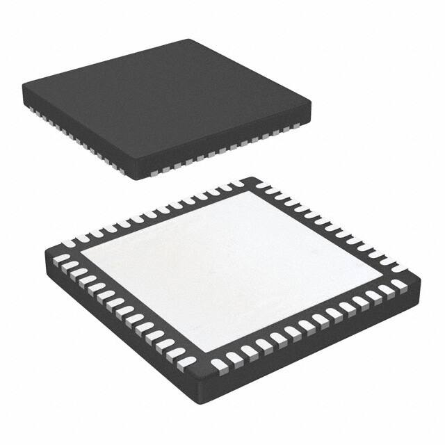


 工商网监
湘ICP备2023018690号
工商网监
湘ICP备2023018690号

