ADC3643
ADC3643
SBAS886 – OCTOBER
2020
SBAS886 – OCTOBER 2020
www.ti.com
ADC364x 14-bit, 10-MSPS to 65-MSPS, Low-Noise, Low Power Dual Channel ADC
1 Features
3 Description
•
•
•
•
The ADC364x family of devices are low-noise, ultralow power, 14-bit, 10-MSPS to 65-MSPS dualchannel, high-speed analog-to-digital converters
(ADCs). Designed for low power consumption, these
devices deliver a noise spectral density of –155
dBFS/Hz, combined with excellent linearity and
dynamic range. The ADC364x offers very good dc
precision, together with IF sampling support, which
make the device an excellent choice for a wide range
of applications. High-speed control loops benefit from
the short latency of only one clock cycle. The ADC
consumes only 72 mW/ch at 65 MSPS, and power
consumption scales well with lower sampling rates.
•
•
•
•
•
•
•
•
•
•
•
Dual channel
14-bit 10/25/65 MSPS ADC
Noise floor: –155 dBFS/Hz
Ultra-low power with optimized power scaling:
29 mW/ch (10 MSPS) to 72 mW/ch (65 MSPS)
Latency: 1 clock cycle
14-Bit, no missing codes
INL: ±0.6 LSB; DNL: ±0.2 LSB
Reference: external or internal
Industrial temperature range: –40°C to +105°C
On-chip digital filter (optional)
– Decimation by 2, 4, 8, 16, 32
– 32-bit NCO
DDR and Serial CMOS interface
Small footprint: 40-VQFN (5 mm × 5 mm) package
Single 1.8-V supply
Spectral performance (fIN = 5 MHz):
– SNR: 79.0 dBFS
– SFDR: 93-dBc HD2, HD3
– SFDR: 101-dBFS worst spur
Spectral performance (fIN = 64 MHz):
– SNR: 74.0 dBFS
– SFDR: 84-dBc HD2, HD3
– SFDR: 90-dBFS worst spur
The ADC364x use a DDR or serial CMOS interface to
output the data offering lowest power digital interface,
together with flexibility to minimize the number of
digital interconnects. These devices are a pin-to-pin
compatible family with different speed grades. These
devices support the extended industrial temperature
range of –40 to +105⁰C.
Device Information
ADC364x
(1)
VQFN (40)
High-speed data acquisition
Industrial monitoring
Thermal imaging
Imaging and sonar
Software defined radio
Power quality
Communications infrastructure
High-speed control loops
Instrumentation
Smart grids
Spectroscopy
Radar
Source measurement unit (SMU)
GPS receiver
Sonar
Substation automation
BODY SIZE (NOM)
5.00 × 5.00 mm
For all available packages, see the package option
addendum at the end of the data sheet.
2 Applications
•
•
•
•
•
•
•
•
•
•
•
•
•
•
•
•
PACKAGE(1)
PART NUMBER
Device Comparison
PART NUMBER
RESOLUTION
SAMPLING RATE
ADC3643
14 BIT
65 MSPS
ADC3642(1)
14 BIT
25 MSPS
ADC3641(1)
14 BIT
10 MSPS
(1)
Product Preview
REFBUF
1.2V REF
Digital Downconverter
VREF
Crosspoint
Switch
NCO
ADC
14bit
AIN
N
DCLK
VCM
0.95V
Dig I/F
CMOS
NCO
DA0..6
DB0..6
BIN
ADC
14bit
N
CLK
ADC364x Block Diagram
An IMPORTANT NOTICE at the end of this data sheet addresses availability, warranty, changes, use in safety-critical applications,
Copyright
© 2020 Texas
Instruments
Incorporated
Submit contains
Document
Feedback
intellectual
property
matters
and other important disclaimers. UNLESS OTHERWISE NOTED, this document
PRODUCTION
DATA.
Product Folder Links: ADC3643
1
�ADC3643
www.ti.com
SBAS886 – OCTOBER 2020
Table of Contents
1 Features............................................................................1
2 Applications..................................................................... 1
3 Description.......................................................................1
4 Revision History.............................................................. 2
5 Pin Configuration and Functions...................................3
6 Specifications.................................................................. 5
6.1 Absolute Maximum Ratings ....................................... 5
6.2 ESD Ratings .............................................................. 5
6.3 Recommended Operating Conditions ........................5
6.4 Thermal Information ...................................................5
6.5 Electrical Characteristics - Power Consumption ........ 6
6.6 Electrical Characteristics - DC Specifications ............ 7
6.7 Electrical Characteristics - AC Specifications
ADC3641 ......................................................................9
6.8 Electrical Characteristics - AC Specifications
ADC3642 ....................................................................10
6.9 Electrical Characteristics - AC Specifications
ADC3643 .................................................................... 11
6.10 Timing Requirements ............................................. 12
6.11 Typical Characteristics - ADC3643......................... 14
7 Parameter Measurement Information.......................... 19
8 Detailed Description......................................................21
8.1 Overview................................................................... 21
8.2 Functional Block Diagram......................................... 21
8.3 Feature Description...................................................22
8.4 Device Functional Modes..........................................42
8.5 Programming............................................................ 43
8.6 Register Maps...........................................................45
9 Application and Implementation.................................. 61
9.1 Typical Application.................................................... 61
10 Initialization Set Up..................................................... 64
10.1 Register Initialization During Operation.................. 64
11 Power Supply Recommendations..............................65
12 Layout...........................................................................67
12.1 Layout Guidelines................................................... 67
12.2 Layout Example...................................................... 67
13 Device and Documentation Support..........................68
13.1 Receiving Notification of Documentation Updates..68
13.2 Support Resources................................................. 68
13.3 Trademarks............................................................. 68
13.4 Electrostatic Discharge Caution..............................68
13.5 Glossary..................................................................68
14 Mechanical, Packaging, and Orderable
Information.................................................................... 68
4 Revision History
NOTE: Page numbers for previous revisions may differ from page numbers in the current version.
2
DATE
REVISION
NOTES
October 2020
*
Initial release.
Submit Document Feedback
Copyright © 2020 Texas Instruments Incorporated
Product Folder Links: ADC3643
�ADC3643
www.ti.com
SBAS886 – OCTOBER 2020
GND
BINP
BINM
GND
AVDD
SCLK
DB0
DB1
DB2
DB3
5 Pin Configuration and Functions
40
39
38
37
36
35
34
33
32
31
PDN/SYNC
1
30
IOVDD
VREF
2
29
DB4
REFGND
3
28
DB5
REFBUF
4
27
DB6
AVDD
5
26
IOGND
CLKP
6
25
DCLK
CLKM
7
24
DA6
VCM
8
23
DA5
RESET
9
22
DA4
21
IOVDD
GND PAD (backside)
13
14
15
16
17
18
AINM
GND
AVDD
SEN
DA0
DA1
19
20
DA3
12
DA2
11
AINP
10
GND
SDIO
Figure 5-1. RSB Package, 40-Pin WQFN, Top View
Table 5-1. Pin Functions
PIN
NAME
NO.
I/O
DESCRIPTION
INPUT/REFERENCE
AINM
13
I
Negative analog input, channel A
AINP
12
I
Positive analog input, channel A
BINP
39
I
Positive analog input, channel B
BINM
38
I
Negative analog input, channel B
REFBUF
4
I
1.2V external voltage reference input for use with internal reference buffer. Internal 100 kΩ
pull-up resistor to AVDD. This pin is also used to configure default operating conditions.
REFGND
3
I
Reference ground input
VCM
8
O
Common-mode voltage output for the analog inputs, 0.95V
VREF
2
I
External voltage reference input
CLKM
7
I
Negative differential sampling clock input for the ADC
CLKP
6
I
Positive differential sampling clock input for the ADC
PDN/SYNC
1
I
Power down/Synchronization input. This pin can be configured via the SPI interface. Active
high. This pin has an internal 21 kΩ pull-down resistor.
RESET
9
I
Hardware reset. Active high. This pin has an internal 21 kΩ pull-down resistor.
CLOCK
CONFIGURATION
Submit Document Feedback
Copyright © 2020 Texas Instruments Incorporated
Product Folder Links: ADC3643
3
�ADC3643
www.ti.com
SBAS886 – OCTOBER 2020
Table 5-1. Pin Functions (continued)
PIN
NAME
NO.
I/O
DESCRIPTION
SCLK
35
I
Serial interface clock input. This pin has an internal 21 kΩ pull-down resistor.
SDIO
10
I
Serial interface data input and output. This pin has an internal 21 kΩ pull-down resistor.
SEN
16
I
Serial interface enable. Active low. This pin has an internal 21 kΩ pull-up resistor to AVDD.
DIGITAL INTERFACE
DA0
17
O
CMOS digital data output.
DA1
18
I/O
CMOS digital data output. Used as FCLK frame clock output for serialized CMOS output
modes. Configured using SPI.
DA2
19
O
CMOS digital data output.
DA3
20
O
CMOS digital data output.
DA4
22
O
CMOS digital data output.
DA5
23
O
CMOS digital data output.
DA6
24
O
CMOS digital data output.
DB0
34
O
CMOS digital data output.
DB1
33
I/O
CMOS digital data output. Used as DCLKIN bit clock input for serialized CMOS output
modes. Configured using SPI.
DB2
32
O
CMOS digital data output.
DB3
31
O
CMOS digital data output.
DB4
29
O
CMOS digital data output.
DB5
28
O
CMOS digital data output.
DB6
27
O
CMOS digital data output.
DCLK
25
O
CMOS output for data bit clock.
AVDD
5,15,36
I
Analog 1.8-V power supply
GND
11,14,37,40,
PowerPAD
I
Ground, 0 V
IOGND
26
I
Ground, 0 V for digital interface
IOVDD
21,30
I
1.8-V power supply for digital interface
POWER SUPPLY
4
Submit Document Feedback
Copyright © 2020 Texas Instruments Incorporated
Product Folder Links: ADC3643
�ADC3643
www.ti.com
SBAS886 – OCTOBER 2020
6 Specifications
6.1 Absolute Maximum Ratings
over operating free-air temperature range (unless otherwise noted)(1)
PARAMETER
TEST CONDITIONS
MIN
MAX
UNIT
Supply voltage range, AVDD, IOVDD
–0.3
2.1
V
Supply voltage range, GND, IOGND, REFGND
–0.3
0.3
V
AINP/M, BINP/M, CLKP/M, DB1 (DCLKIN)
Voltage applied to
VREF, REFBUF
input pins
PDN, RESET, SCLK, SEN, SDIO
–0.3
2.1
–0.3
2.1
–0.3
2.1
Junction temperature, TJ
Storage temperature, Tstg
(1)
V
–65
105
°C
150
°C
Stresses beyond those listed under Absolute Maximum Ratings may cause permanent damage to the device. These are stress ratings
only, which do not imply functional operation of the device at these or any other conditions beyond those indicated under
Recommended Operating Conditions. Exposure to absolute-maximum-rated conditions for extended periods may affect device
reliability.
6.2 ESD Ratings
VALUE
V(ESD)
(1)
(2)
Electrostatic discharge
Human body model (HBM), per ANSI/ESDA/JEDEC
JS-001, all pins(1)
2500
Charged device model (CDM), per JEDEC
specification JESD22-C101, all pins(2)
1000
UNIT
V
JEDEC document JEP155 states that 500-V HBM allows safe manufacturing with a standard ESD control process.
JEDEC document JEP157 states that 250-V CDM allows safe manufacturing with a standard ESD control process.
6.3 Recommended Operating Conditions
over operating free-air temperature range (unless otherwise noted)
Supply voltage range
TA
Operating free-air temperature
TJ
Operating junction temperature
(1)
(2)
MIN
NOM
MAX
UNIT
AVDD(1)
1.75
1.8
1.85
V
IOVDD(1)
1.75
1.8
1.85
V
–40
105
°C
105(2)
°C
Measured to GND.
Prolonged use above this junction temperature may increase the device failure-in-time (FIT) rate.
6.4 Thermal Information
ADC364x
THERMAL METRIC
RSB (QFN)
UNIT
40 Pins
RΘJA
Junction-to-ambient thermal resistance
30.7
°C/W
RΘJC(top)
Junction-to-case (top) thermal resistance
16.4
°C/W
RΘJB
Junction-to-board thermal resistance
10.5
°C/W
ΨJT
Junction-to-top characterization parameter
0.2
°C/W
ΨJB
Junction-to-board characterization parameter
10.5
°C/W
RΘJC(bot)
Junction-to-case (bottom) thermal resistance
2.0
°C/W
Submit Document Feedback
Copyright © 2020 Texas Instruments Incorporated
Product Folder Links: ADC3643
5
�ADC3643
www.ti.com
SBAS886 – OCTOBER 2020
6.5 Electrical Characteristics - Power Consumption
Typical values are over the operating free-air temperature range, at TA = 25°C, full temperature range is TMIN = –40°C to T
= 105°C, ADC sampling rate = 65 MSPS, 50% clock duty cycle, AVDD, IOVDD = 1.8 V, external 1.6V reference, 5 pF
output load, and –1-dBFS differential input, unless otherwise noted
MAX
PARAMETER
TEST CONDITIONS
MIN
TYP
MAX
UNIT
ADC3641 - 10 MSPS
IAVDD
Analog supply current
current(1)
IIOVDD
I/O supply
PDIS
Power dissipation(1)
IIOVDD
I/O supply current(1)
External reference
DDR CMOS
External reference, DDR CMOS
27
mA
5
58
Serial CMOS 2-wire
TBD
Serial CMOS 1-wire
TBD
4x complex decimation, Serial CMOS
2-wire
TBD
mW
mA
ADC3642 - 25 MSPS
IAVDD
Analog supply current
current(1)
IIOVDD
I/O supply
PDIS
Power dissipation(1)
IIOVDD
I/O supply current(1)
External reference
DDR CMOS
External reference, DDR CMOS
31
mA
8
70
Serial CMOS 2-wire
TBD
4x complex decimation, Serial CMOS
2-wire
TBD
mW
mA
ADC3643 - 65 MSPS
IAVDD
Analog supply current
current(1)
IIOVDD
I/O supply
PDIS
Power dissipation(1)
External reference
64
78
DDR CMOS
16
20
144
176
External reference, DDR CMOS
8x complex decimation, Serial CMOS
2-wire
19
16x complex decimation, Serial CMOS
1-wire
17
IIOVDD
32x complex decimation, Serial CMOS
1-wire
15
IIOVDD
32x complex decimation, Serial CMOS
1/2-wire
16
IIOVDD
IIOVDD
I/O supply
current(1)
mA
mW
mA
MISCELLANEOUS
Internal reference, additional analog
supply current
IAVDD
External 1.2V reference (REFBUF),
additional analog supply current
Single ended clock input, reduces
analog supply current by
PDIS
(1)
6
Power consumption in global power
down mode
FS = 10 MSPS
1
FS = 25 MSPS
1.5
FS = 65 MSPS
3
mA
0.3
Enabled via SPI
0.7
Default power down mask, internal
reference
5
Default power down mask, external
reference
9
mW
Measured with a 2 MHz input frequency full-scale sine wave at specified sample rate, with ~ 5 pF loading on each CMOS output pin.
Submit Document Feedback
Copyright © 2020 Texas Instruments Incorporated
Product Folder Links: ADC3643
�ADC3643
www.ti.com
SBAS886 – OCTOBER 2020
6.6 Electrical Characteristics - DC Specifications
Typical values are over the operating free-air temperature range, at TA = 25°C, full temperature range is TMIN = –40°C to T
MAX = 105°C, ADC sampling rate = 65 MSPS, 50% clock duty cycle, AVDD, IOVDD = 1.8 V, external 1.6V reference, 5 pF
output load, and –1-dBFS differential input, unless otherwise noted
PARAMETER
TEST CONDITIONS
MIN
TYP
MAX
UNIT
DC ACCURACY
No missing codes
PSRR
14
FIN = 1 MHz
bits
50
dB
ADC3641 - 10 MSPS: DC ACCURACY
DNL
Differential nonlinearity
FIN = 5 MHz
TBD
± 0.1
± 0.25
LSB
INL
Integral nonlinearity
FIN = 5 MHz
TBD
± 0.6
± 0.8
LSB
VOS_ERR
Offset error
TBD
8
TBD
VOS_DRIFT
Offset drift over temperature
TBD
TBD
0.1
LSB
LSB/ºC
GAINERR
Gain error
External 1.6 V reference
TBD
0.05
TBD
%FSR
GAINDRIFT
Gain drift over temperature
External 1.6 V reference
TBD
TBD
10
ppm/ºC
GAINERR
Gain error
Internal reference
TBD
TBD
TBD
%FSR
GAINDRIFT
Gain drift over temperature
Internal reference
TBD
TBD
TBD
dB
Transition Noise
0.6
LSBRMS
ADC3642 - 25 MSPS: DC ACCURACY
DNL
Differential nonlinearity
FIN = 5 MHz
TBD
± 0.1
± 0.25
LSB
INL
Integral nonlinearity
FIN = 5 MHz
TBD
± 0.6
± 0.8
LSB
VOS_ERR
Offset error
TBD
8
TBD
VOS_DRIFT
Offset drift over temperature
TBD
TBD
0.1
LSB
LSB/ºC
GAINERR
Gain error
External 1.6 V reference
TBD
0.05
TBD
%FSR
GAINDRIFT
Gain drift over temperature
External 1.6 V reference
TBD
TBD
10
ppm/ºC
GAINERR
Gain error
Internal reference
TBD
TBD
TBD
%FSR
GAINDRIFT
Gain drift over temperature
Internal reference
TBD
TBD
TBD
Transition Noise
0.6
dB
LSBRMS
ADC3643 - 65 MSPS: DC ACCURACY
DNL
Differential nonlinearity
FIN = 5 MHz
-0.35
± 0.2
0.35
LSB
INL
Integral nonlinearity
FIN = 5 MHz
-1.25
± 0.6
1.25
LSB
VOS_ERR
Offset error
35
0
35
LSB
VOS_DRIFT
Offset drift over temperature
GAINERR
Gain error
External 1.6 V reference
GAINDRIFT
Gain drift over temperature
External 1.6 V reference
GAINERR
Gain error
Internal reference
GAINDRIFT
Gain drift over temperature
Internal reference
131
ppm/ºC
0.6
LSBRMS
2.25
Vpp
Transition Noise
-1
LSB/ºC
0.6
%FSR
-5
ppm/ºC
0.8
%FSR
ADC ANALOG INPUT (AINP/M, BINP/M)
FS
Input full scale
Default, differential
VCM
Input common mode voltage
RIN
Differential input resistance
FIN = 100 kHz
CIN
Differential input capacitance
FIN = 100 kHz
VOCM
Output common mode voltage
BW
Analog input bandwidth (-3dB)
900
MHz
0.9
0.95
1.0
V
8
Ω
7
pF
0.95
V
Submit Document Feedback
Copyright © 2020 Texas Instruments Incorporated
Product Folder Links: ADC3643
7
�ADC3643
www.ti.com
SBAS886 – OCTOBER 2020
6.6 Electrical Characteristics - DC Specifications (continued)
Typical values are over the operating free-air temperature range, at TA = 25°C, full temperature range is TMIN = –40°C to T
MAX = 105°C, ADC sampling rate = 65 MSPS, 50% clock duty cycle, AVDD, IOVDD = 1.8 V, external 1.6V reference, 5 pF
output load, and –1-dBFS differential input, unless otherwise noted
PARAMETER
TEST CONDITIONS
MIN
TYP
MAX
UNIT
Internal Voltage Reference
VREF
Internal reference voltage
VREF Output Impedance
1.6
V
8
Ω
1.2
V
Reference Input Buffer (REFBUF)
External reference voltage
External voltage reference (VREF)
1.6
V
Input Current
VREF
External voltage reference
0.3
mA
Input impedance
5.3
kΩ
Clock Input (CLKP/M)
Input clock frequency
0.5
VID
Differential input voltage
1
VCM
Input common mode voltage
RIN
Single ended input resistance to common mode
CIN
Single ended input capacitance
65
MHz
3.6
Vpp
0.9
V
5
kΩ
1.5
Clock duty cycle
40
50
pF
60
%
Digital Inputs (RESET, PDN, SCLK, SEN, SDIO)
VIH
High level input voltage
VIL
Low level input voltage
IIH
High level input current
IIL
Low level input current
CI
Input capacitance
1.4
0.4
90
-150
150
90
1.5
V
uA
pF
Digital Output (SDOUT)
VOH
High level output voltage
ILOAD = -400 uA
VOL
Low level output voltage
ILOAD = 400 uA
IOVDD
– 0.1
IOVDD
V
0.1
CMOS Interface (DA0:DA6, DB0:DB6)
Output data rate
8
per CMOS output pin
VOH
High level output voltage
ILOAD = -400 uA
VOL
Low level output voltage
ILOAD = 400 uA
VIH
High level input voltage
VIL
Low level input voltage
Input clock (Serial CMOS)
250
IOVDD
– 0.1
IOVDD
MHz
V
0.1
IOVDD
– 0.1
IOVDD
V
0.1
Submit Document Feedback
Copyright © 2020 Texas Instruments Incorporated
Product Folder Links: ADC3643
�ADC3643
www.ti.com
SBAS886 – OCTOBER 2020
6.7 Electrical Characteristics - AC Specifications ADC3641
Typical values are over the operating free-air temperature range, at TA = 25°C, full temperature range is TMIN = –40°C to T
MAX = 105°C, ADC sampling rate = 10 MSPS, external reference, 50% clock duty cycle, AVDD, IOVDD = 1.8 V, external 1.6V
reference, 5 pF output load, and –1-dBFS differential input, unless otherwise noted
PARAMETER
TEST CONDITIONS
MIN
TYP
MAX
UNIT
ADC3641: 10 MSPS
NSD
Noise Spectral Density
SNR
Signal to noise ratio
fIN = 1.1 MHz, AIN = -20 dBFS
-146.0
fIN = 1.1 MHz
SINAD
Signal to noise and distortion ratio
fIN = 4.9 MHz
79.0
TBD
78.0
fIN = 1.1 MHz
TBD
TBD
fIN = 9.9 MHz
THD
Effective number of bits
Total Harmonic Distortion (First five
harmonics)
fIN = 4.9 MHz
Non HD2,3
Spur free dynamic range including
second and third harmonic distortion
Spur free dynamic range (excluding
HD2 and HD3)
12.6
fIN = 1.1 MHz
TBD
TBD
fIN = 4.9 MHz
Two tone inter-modulation distortion
TBD
90
90
fIN = 1.1 MHz
95
f1 = 1 MHz, f2 = 2 MHz, AIN = -7 dBFS/
tone
dBc
90
TBD
fIN = 9.9 MHz
fIN = 4.9 MHz
bit
TBD
fIN = 1.1 MHz
fIN = 9.9 MHz
IMD3
12.8
fIN = 9.9 MHz
fIN = 4.9 MHz
dBFS
12.8
TBD
fIN = 9.9 MHz
SFDR
TBD
dBFS
TBD
fIN = 1.1 MHz
ENOB
79.0
fIN = 9.9 MHz
fIN = 4.9 MHz
dBFS/Hz
TBD
95
dBc
dBFS
95
TBD
dBc
Submit Document Feedback
Copyright © 2020 Texas Instruments Incorporated
Product Folder Links: ADC3643
9
�ADC3643
www.ti.com
SBAS886 – OCTOBER 2020
6.8 Electrical Characteristics - AC Specifications ADC3642
Typical values are over the operating free-air temperature range, at TA = 25°C, full temperature range is TMIN = –40°C to T
MAX = 105°C, ADC sampling rate = 25 MSPS, external reference, 50% clock duty cycle, AVDD, IOVDD = 1.8 V, external 1.6V
reference, 5 pF output load, and –1-dBFS differential input, unless otherwise noted
PARAMETER
TEST CONDITIONS
MIN
TYP
MAX
UNIT
ADC3642: 25 MSPS
NSD
Noise Spectral Density
fIN = 1.1 MHz, AIN = -20 dBFS
-151.0
fIN = 1.1 MHz
fIN = 5 MHz
SNR
Signal to noise ratio
Signal to noise and distortion ratio
79.0
TBD
78.4
fIN = 20 MHz
77.0
fIN = 40 MHz
76.0
fIN = 1.1 MHz
TBD
TBD
TBD
fIN = 20 MHz
TBD
fIN = 40 MHz
TBD
fIN = 5 MHz
Effective number of bits
Total Harmonic Distortion (First five
harmonics)
THD
SFDR
Spur free dynamic range including
second and third harmonic distortion
12.7
12.5
fIN = 40 MHz
12.3
fIN = 1.1 MHz
TBD
TBD
TBD
fIN = 20 MHz
TBD
fIN = 40 MHz
TBD
fIN = 1.1 MHz
90
TBD
Non HD2,3
IMD3
10
Two tone inter-modulation distortion
90
fIN = 20 MHz
88
fIN = 40 MHz
85
dBc
95
TBD
95
fIN = 10 MHz
95
fIN = 20 MHz
95
fIN = 40 MHz
95
f1 = 1 MHz, f2 = 2 MHz, AIN = -7 dBFS/
tone
TBD
f1 = 10 MHz, f2 = 12 MHz, AIN = -7
dBFS/tone
TBD
Submit Document Feedback
dBc
90
fIN = 10 MHz
fIN = 5 MHz
bit
TBD
fIN = 10 MHz
fIN = 1.1 MHz
Spur free dynamic range (excluding
HD2 and HD3)
12.8
fIN = 20 MHz
fIN = 5 MHz
dBFS
12.8
TBD
fIN = 10 MHz
fIN = 5 MHz
dBFS
TBD
fIN = 10 MHz
fIN = 1.1 MHz
ENOB
79.0
fIN = 10 MHz
fIN = 5 MHz
SINAD
dBFS/Hz
dBFS
dBc
Copyright © 2020 Texas Instruments Incorporated
Product Folder Links: ADC3643
�ADC3643
www.ti.com
SBAS886 – OCTOBER 2020
6.9 Electrical Characteristics - AC Specifications ADC3643
Typical values are over the operating free-air temperature range, at TA = 25°C, full temperature range is TMIN = –40°C to T
MAX = 105°C, ADC sampling rate = 65 MSPS, external reference, 50% clock duty cycle, AVDD, IOVDD = 1.8 V, external 1.6V
reference, 5 pF output load, and –1-dBFS differential input, unless otherwise noted
PARAMETER
TEST CONDITIONS
MIN
TYP
MAX
UNIT
ADC3643: 65 MSPS
NSD
Noise Spectral Density
fIN = 1.1 MHz, AIN = -20 dBFS
-155.0
fIN = 1.1 MHz
fIN = 5 MHz
SNR
Signal to noise ratio
79.0
77.0
79.0
fIN = 20 MHz
78.8
fIN = 40 MHz
77.0
fIN = 64 MHz
74.0
fIN = 1.1 MHz
SINAD
Signal to noise and distortion ratio
Effective number of bits
78.9
fIN = 20 MHz
78.0
fIN = 40 MHz
76.0
fIN = 64 MHz
73.4
Total Harmonic Distortion (First five
harmonics)
12.8
fIN = 20 MHz
12.8
fIN = 40 MHz
12.5
fIN = 64 MHz
12.0
Spur free dynamic range including
second and third harmonic distortion
Non HD2,3
IMD3
Spur free dynamic range (excluding
HD2 and HD3)
Two tone inter-modulation distortion
91
91
fIN = 20 MHz
85
fIN = 40 MHz
82
fIN = 64 MHz
81
fIN = 1.1 MHz
90
88
95
fIN = 20 MHz
88
fIN = 40 MHz
83
fIN = 64 MHz
84
fIN = 1.1 MHz
100
93
dBc
93
fIN = 10 MHz
fIN = 5 MHz
bit
88
84
fIN = 10 MHz
fIN = 5 MHz
SFDR
12.8
fIN = 10 MHz
fIN = 5 MHz
dBFS
12.8
12.4
fIN = 1.1 MHz
THD
79.0
fIN = 10 MHz
fIN = 5 MHz
dBFS
79.0
76.2
fIN = 1.1 MHz
ENOB
79.0
fIN = 10 MHz
fIN = 5 MHz
dBFS/Hz
dBc
101
fIN = 10 MHz
98
fIN = 20 MHz
95
fIN = 40 MHz
94
fIN = 64 MHz
90
f1 = 10 MHz, f2 = 12 MHz, AIN = -7
dBFS/tone
92
dBFS
dBc
Submit Document Feedback
Copyright © 2020 Texas Instruments Incorporated
Product Folder Links: ADC3643
11
�ADC3643
www.ti.com
SBAS886 – OCTOBER 2020
6.10 Timing Requirements
Typical values are over the operating free-air temperature range, at TA = 25°C, full temperature range is TMIN = –40°C to T
MAX = 105°C, ADC sampling rate = 65 MSPS, 50% clock duty cycle, AVDD, IOVDD = 1.8 V, and –1-dBFS differential input,
unless otherwise noted
PARAMETER
TEST CONDITIONS
MIN
NOM
MAX
UNIT
ADC Timing Specifications
tAD
Aperture delay
0.85
tA
Aperture jitter
Square wave clock with fast edges
tJ
Jitter on DCLKIN
Serial CMOS output mode
Recory time from +6 dB overload condition
Signal conversion period, referenced to
sampling clock falling edge
tCONV
Time to valid data after coming out of power
down. Internal reference.
Wake up
time
Time to valid data after coming out of power
down. External 1.6V reference.
tS,SYNC
Setup time for SYNC input signal
tH,SYNC
Hold time for SYNC input signal
ADC
Latency
180
FS = 10 Msps
-TS/2
FS = 25 Msps
-TS/2
FS = 65 Msps
-TS/4
FS = 10 Msps
+TS ×
1/5
FS = 25 Msps
+TS ×
3/8
FS = 65 Msps
+TS ×
5/8
Bandgap reference enabled, single ended
clock
14.6
Bandgap reference enabled, differential clock
14.0
Bandgap reference disabled, single ended
clock
1.7
Bandgap reference disabled, differential clock
2.1
Bandgap reference enabled, single ended
clock
14.6
Bandgap reference enabled, differential clock
14.0
Bandgap reference disabled, single ended
clock
1.8
Bandgap reference disabled, differential clock
1.7
Add.
Latency
Sampling
Clock
Period
Sampling
Clock
Period
us
ms
us
ms
500
ps
600
DDR CMOS
1
Serialized CMOS: 2-wire
2
Serialized CMOS: 1-wire
1
Serialized CMOS: 1/2-wire
ps
Clock
cycle
1
Referenced to sampling clock rising edge
Signal input to data output
fs
± 50
SNR within 1 dB of expected value
Signal acquisition period, referenced to
sampling clock falling edge
tACQ
ns
Clock
cycles
1
Real decimation by 2
21
Complex decimation by 2
22
Real or complex decimation by 4, 8, 16, 32
23
Output
clock
cycles
INTERFACE TIMING - PARALLEL DDR CMOS
tPD
Propagation delay: sampling clock falling
edge to DCLK rising edge
tCD
DCLK rising edge to output data delay
tDV
Data valid, DDR CMOS
3
5
Fout = 10 MSPS
-0.70
-0.32
Fout = 25 MSPS
-0.68
-0.30
-0.31
Fout = 65 MSPS
-0.73
Fout = 10 MSPS
49.35 49.93
Fout = 25 MSPS
19.66 19.77
Fout = 65 MSPS
12
Submit Document Feedback
7.42
7
ns
ns
ns
7.51
Copyright © 2020 Texas Instruments Incorporated
Product Folder Links: ADC3643
�ADC3643
www.ti.com
SBAS886 – OCTOBER 2020
6.10 Timing Requirements (continued)
Typical values are over the operating free-air temperature range, at TA = 25°C, full temperature range is TMIN = –40°C to T
= 105°C, ADC sampling rate = 65 MSPS, 50% clock duty cycle, AVDD, IOVDD = 1.8 V, and –1-dBFS differential input,
unless otherwise noted
MAX
PARAMETER
TEST CONDITIONS
MIN
NOM
MAX
UNIT
INTERFACE TIMING - SERIAL CMOS
tPD
Delay between sampling clock falling edge to
DCLKIN falling edge < 2.5ns.
2+T 3+T 4+T
TDCLK = DCLK period
DCLK + DCLK + DCLK +
tCDCLK = Sampling clock falling edge to
tCDCLK tCDCLK tCDCLK
DCLKIN falling edge
Propagation delay: sampling clock falling
edge to DCLK rising edge
Delay between sampling clock falling edge to
DCLKIN falling edge >= 2.5ns.
TDCLK = DCLK period
tCDCLK = Sampling clock falling edge to
DCLKIN falling edge
DCLK rising edge to output data delay,
2-wire serial CMOS
tCD
DCLK rising edge to output data delay,
1-wire series CMOS
DCLK rising edge to output data delay, 1/2wire serial CMOS
Data valid, 2-wire serial CMOS
tDV
2+t
3+t
4+t
CDCLK
CDCLK
CDCLK
Fout = 10 MSPS, DA/B5,6 = 80 MBPS
-0.24
0.10
Fout = 20 MSPS, DA/B5,6 = 160 MBPS
-0.29
0.10
Fout = 30 MSPS, DA/B5,6 = 240 MBPS
-0.28
0.09
Fout = 5 MSPS, DA/B6 = 80 MBPS
-0.22
0.11
Fout = 10 MSPS, DA/B6 = 160 MBPS
-0.27
0.11
Fout = 15 MSPS, DA/B6 = 240 MBPS
-0.52
0.08
Fout = 5 MSPS, DA6 = 160 MBPS
-0.24
0.10
Fout = 10 MSPS, DA/B5,6 = 80 MBPS
12.19 12.36
Fout = 20 MSPS, DA/B5,6 = 160 MBPS
5.93
6.1
Fout = 30 MSPS, DA/B5,6 = 240 MBPS
3.91
4.07
Fout = 5 MSPS, DA/B6 = 80 MBPS
ns
ns
12.21 12.39
Data valid, 1-wire serial CMOS
Fout = 10 MSPS, DA/B6 = 160 MBPS
5.95
Fout = 15 MSPS, DA/B6 = 240 MBPS
3.83
4.08
Data valid, 1/2-wire serial CMOS
Fout = 5 MSPS, DA6 = 160 MBPS
5.36
6.13
ns
6.1
SERIAL PROGRAMMING INTERFACE (SCLK, SEN, SDIO) - Input
fCLK(SCLK) Serial clock frequency
tSU(SEN)
SEN to rising edge of SCLK
tH(SEN)
SEN from rising edge of SCLK
tSU(SDIO)
SDIO to rising edge of SCLK
tH(SDIO)
SDIO from rising edge of SCLK
20
MHz
10
9
ns
17
9
SERIAL PROGRAMMING INTERFACE (SDIO) - Output
t(OZD)
SDIO tri-state to driven
3.9
10.8
t(ODZ)
SDIO data to tri-state
3.4
14
t(OD)
SDIO valid from falling edge of SCLK
3.9
10.8
ns
Submit Document Feedback
Copyright © 2020 Texas Instruments Incorporated
Product Folder Links: ADC3643
13
�ADC3643
www.ti.com
SBAS886 – OCTOBER 2020
6.11 Typical Characteristics - ADC3643
0
0
-20
-20
-40
-40
Amplitude (dBFS)
Amplitude (dBFS)
Typical values at T A = 25 °C, ADC sampling rate F S = 65 MSPS, AIN = –1 dBFS differential input, AVDD =
IOVDD = 1.8 V, 65k FFT, external 1.6 V reference, 5 pF output load, unless otherwise noted.
-60
-80
-60
-80
-100
-100
-120
-120
-140
-140
0
10
20
Input Frequency (MHz)
0
30
10
20
Input Frequency (MHz)
30
D002
D001
Figure 6-2. Single Tone FFT at FIN = 10 MHz
0
0
-20
-20
-40
-40
Amplitude (dBFS)
Amplitude (dBFS)
Figure 6-1. Single Tone FFT at FIN = 1.1 MHz
-60
-80
-60
-80
-100
-100
-120
-120
-140
-140
0
10
20
Input Frequency (MHz)
0
30
10
20
Input Frequency (MHz)
30
D004
D003
Figure 6-4. Single Tone FFT at FIN = 40 MHz
AIN = -20 dBFS
0
0
-20
-20
-40
-40
Amplitude (dBFS)
Amplitude (dBFS)
Figure 6-3. Single Tone FFT at FIN = 10 MHz
-60
-80
-60
-80
-100
-100
-120
-120
-140
-140
0
10
20
Input Frequency (MHz)
30
0
10
20
Input Frequency (MHz)
30
D005
Figure 6-5. Single Tone FFT at FIN = 64 MHz
14
D006
Figure 6-6. Single Tone FFT at FIN = 90 MHz
Submit Document Feedback
Copyright © 2020 Texas Instruments Incorporated
Product Folder Links: ADC3643
�ADC3643
SBAS886 – OCTOBER 2020
0
0
-20
-20
-40
-40
Amplitude (dBFS)
Amplitude (dBFS)
www.ti.com
-60
-80
-60
-80
-100
-100
-120
-120
-140
-140
0
10
20
Input Frequency (MHz)
30
0
10
20
Input Frequency (MHz)
30
D008
D009
AIN = -7 dBFS/tone
AIN = -20 dBFS/tone
Figure 6-7. Two Tone FFT at FIN = 10/12 MHz
85
13
Ext REF
Int REF
SNR, int REF
SFDR, int REF
Non HD23, int REF
12.8
105
SFDR, Non HD23 (dBc)
SNR, ext REF
SFDR, ext REF
Non HD23, ext REF
83
12.6
81
100
79
95
77
90
75
85
12
80
70
11.8
73
0
10
20
30
40
50
Input Frequency (MHz)
60
ENOB (bit)
SNR (dBFS)
Figure 6-8. Two Tone FFT at FIN = 10/12 MHz
110
12.4
12.2
0
10
20
30
40
50
Input Frequency (MHz)
60
70
D021
D020
Figure 6-10. ENOB vs Input Frequency
Figure 6-9. AC Performance vs Input Frequency
81.5
105
SNR
SFDR
SFDR
Non HD23
80
110
79.5
105
79
100
75
80
60
79.5
45
30
-70
-60
-50
-40
-30
-20
Input Amplitude (dBFS)
-10
0
78.5
95
78
90
77.5
85
77
10
15
20
25 30 35 40 45 50
ADC Sampling Rate (MSPS)
D026
55
60
SFDR, Non HD23 (dBc)
80.5
SNR (dBFS)
90
SFDR, Non HD23 (dBc)
SNR (dBFS)
115
SNR
81
79
-80
80.5
Non HD23
80
65
D029
FIN = 5 MHz
FIN = 5 MHz
Figure 6-11. AC Performance vs Input Amplitude
Figure 6-12. AC Performance vs Sampling Rate
Submit Document Feedback
Copyright © 2020 Texas Instruments Incorporated
Product Folder Links: ADC3643
15
�ADC3643
www.ti.com
SBAS886 – OCTOBER 2020
120
110
78.5
105
78
100
77.5
95
77
90
76.5
85
0.5
1
1.5
2
Clock Amplitude (Vpp)
2.5
100
SNR (dBFS)
SINAD (dBFS)
SFDR (dBc)
115
79
0
80
79.5
95
79
90
78.5
85
SNR/SINAD (dBFS)
SNR (dBFS)
79.5
SNR, FIN = 10 MHz
SFDR, FIN = 10 MHz
SFDR (dBc)
SNR, FIN = 5 MHz
SFDR, FIN = 5 MHz
78
1.7
1.75
3
1.8
AVDD (V)
SFDR (dBc)
80
80
1.9
1.85
D041
FIN = 5 MHz
D030
Figure 6-13. AC Performance vs Clock Amplitude
Figure 6-14. AC Performance vs AVDD
80.5
110
95
78.5
90
85
0.975
79.5
95
79
90
78.5
85
78
35
1
40
45
50
55
60
Clock Duty Cycle (%)
D048
65
SFDR (dBc)
79
0.95
VCM (V)
SFDR
105
100
0.925
100
SNR
79.5
78
0.9
80
SNR (dBFS)
SNR (dBFS)
80
SFDR, -40qC
SFDR, 25qC
SFDR, 105qC
SFDR (dBc)
SNR, -40qC
SNR, 25qC
SNR, 105qC
80
70
D051
FIN = 5 MHz
FIN = 5 MHz
Figure 6-15. AC Performance vs VCM vs
Temperature
Figure 6-16. AC Performance vs Clock Duty Cycle
1
110
ChA Victim
ChB Victim
Ext REF
INT REF
Integral Nonlinearity (LSB)
Isolation (dBc)
105
100
95
90
0.5
0
-0.5
85
80
0
10
20
30
40 50 60 70 80
Input Frequency (MHz)
90
-1
100 110 120
0
2048
D053
4096
6144
8192
Code
10240 12288 14336 16384
D054
Figure 6-17. Isolation vs Input Frequency
FIN = 5 MHz
Figure 6-18. INL vs Code
16
Submit Document Feedback
Copyright © 2020 Texas Instruments Incorporated
Product Folder Links: ADC3643
�ADC3643
www.ti.com
SBAS886 – OCTOBER 2020
0.5
100
Ext REF
Int REF
90
0.3
80
0.2
70
Code Occurance (%)
Differential Nonlinearity (LSB)
0.4
0.1
0
-0.1
-0.2
60
50
40
30
20
-0.3
10
-0.4
0
-0.5
0
2048
4096
6144
8192
Code
8195
10240 12288 14336 16384
8196
8197
8198
Output Code
8199
8200
D061
D066
Figure 6-20. DC Histogram
FIN = 5 MHz
Figure 6-19. DNL vs Code
80
24
IAVDD, ADC3641/42
IAVDD, ADC3643
IIOVDD, DDR
75
70
IIOVDD, 2-w
IIOVDD, 1-w
IIOVDD, 1/2-w
22
20
65
12288
18
IAVDD (mA)
Output Code
60
8192
4096
16
ADC3643
55
14
50
12
45
10
40
8
35
6
30
4
ADC3641/42
25
2
20
0
0
10000
20000
30000 40000
Samples
50000
60000
70000
IIOVDD (mA)
16384
5
10
15
20
25 30 35 40 45
Sampling Rate (MSPS)
50
55
60
0
65
D065
D064
FIN = 1 MHz
Pulse input = 1 MHz
Figure 6-21. Pulse Response
Figure 6-22. Current vs Sampling Rate
Submit Document Feedback
Copyright © 2020 Texas Instruments Incorporated
Product Folder Links: ADC3643
17
�ADC3643
www.ti.com
SBAS886 – OCTOBER 2020
27.5
35
Bypass (DDR)
/4 Real (2-w)
/8 Real (2-w)
/32 Real (2-w)
25
22.5
/2 Real (2-w)
/4 Complex (2-w)
/8 Complex (2-w)
/32 Complex (2-w)
25
20
17.5
IIOVDD (mA)
IIOVDD (mA)
CL = 5 pF
CL = 10 pF
CL = 15 pF
CL = 22 pF
30
15
12.5
10
20
15
10
7.5
5
5
0
2.5
5
10
15
20
25 30 35 40 45
Sampling Rate (MSPS)
50
55
60
65
5
10
D066
20
25 30 35 40 45
Sampling Rate (MSPS)
50
55
60
65
D067
FIN = 1 MHz
FIN = 1 MHz
Figure 6-23. IIOVDD Current vs Decimation
18
15
Figure 6-24. IIOVDD Current vs Load Capacitance
Submit Document Feedback
Copyright © 2020 Texas Instruments Incorporated
Product Folder Links: ADC3643
�ADC3643
www.ti.com
SBAS886 – OCTOBER 2020
7 Parameter Measurement Information
Sample N
Input Signal
Sample N+1
tAD
tPD
Sampling
Clock
tACQ
tCONV
tCD
TDCLK
DCLK
tDV
D13
D6
D13
D6
D13
DA0
D7
D0
D7
D0
D7
DB6
D13
D6
D13
D6
D13
D7
D0
D7
D0
D7
...
...
DA6
DB0
Sample N-2
Sample N-1
Sample N
Figure 7-1. Timing diagram: DDR CMOS
Sample N
Input Signal
Sample N+1
tAD
tPD
Sampling
Clock
tACQ
tCONV
tCDCLK
DCLKIN
DCLK
tCD
TDCLK
FCLK
tDV
DA6
D13
D11
D9
D7
D5
D3
D1
D13
D11
D9
D7
D5
D3
D1
DA5
D12
D10
D8
D6
D4
D2
D0
D12
D10
D8
D6
D4
D2
D0
DB6
D13
D11
D9
D7
D5
D3
D1
D13
D11
D9
D7
D5
D3
D1
DB5
D12
D10
D8
D6
D4
D2
D0
D12
D10
D8
D6
D4
D2
D0
Sample N-2
Sample N-1
Figure 7-2. Timing diagram: 2-wire serial CMOS
Submit Document Feedback
Copyright © 2020 Texas Instruments Incorporated
Product Folder Links: ADC3643
19
�ADC3643
www.ti.com
SBAS886 – OCTOBER 2020
Sample N
Input Signal
Sample N+1
tAD
tPD
Sampling
Clock
tACQ
tCONV
tCDCLK
DCLKIN
DCLK
tCD
TDCLK
FCLK
tDV
DA6
D2
D1
D0
D13
D12
D11
D10
D9
D8
D7
D6
D5
D4
D3
D2
D1
D0
DB6
D2
D1
D0
D13
D12
D11
D10
D9
D8
D7
D6
D5
D4
D3
D2
D1
D0
Sample N-2
Sample N-1
Figure 7-3. Timing diagram: 1-wire serial CMOS
Sample N
Input Signal
Sample N+1
tAD
tPD
Sampling
Clock
tACQ
tCONV
tCDCLK
DCLKIN
(DB1)
TDCLK
DCLK
tCD
FCLK
(DA1)
tDV
Channel A
DA6
Channel B
D D D D D D D D D D D D D D D D D D D D D D D D D D D D D D D D D D
5 4 3 2 1 0 13 12 11 10 9 8 7 6 5 4 3 2 1 0 13 12 11 10 9 8 7 6 5 4 3 2 1 0
Sample N-2
Sample N-1
Figure 7-4. Timing diagram: 1/2-wire serial CMOS
20
Submit Document Feedback
Copyright © 2020 Texas Instruments Incorporated
Product Folder Links: ADC3643
�ADC3643
www.ti.com
SBAS886 – OCTOBER 2020
8 Detailed Description
8.1 Overview
The ADC364x is a low noise, ultra-low power 14-bit high-speed dual channel ADC family supporting sampling
rates from 10 to 65 Msps. It offers very good DC precision together with IF sampling support which makes it
ideally suited for a wide range of applications. The ADC364x is equipped with an on-chip internal reference
option but it also supports the use of an external, high precision 1.6 V voltage reference or an external 1.2 V
reference which is buffered and gained up internally. Because of the inherent low latency architecture, the digital
output result is available after only one clock cycle. Single ended as well as differential input signaling is
supported.
An optional programmable digital down converter enables external anti-alias filter relaxation as well as output
data rate reduction. The digital filter provides a 32-bit programmable NCO and supports both real or complex
decimation.
The ADC364x family uses a parallel DDR CMOS as well as a 2-wire, 1-wire and 1/2-wire serial CMOS interface
to output the data offering lowest power digital interface together with the flexibility to minimize the number of
digital interconnects. The ADC364x includes a digital output formatter which supports output resolutions from 14
to 20-bit. The device is a pin-to-pin compatible family with different speed grades.
The device features and control options can be set up either through pin configurations or via SPI register writes.
8.2 Functional Block Diagram
REFBUF
1.2 V REF
Digital Downconverter
VREF
Crosspoint
Switch
NCO
ADC
14 bit
AIN
N
DCLK
VCM
0.95 V
Dig I/F
CMOS
NCO
BIN
DA0..6
DB0..6
ADC
14 bit
N
CLK
SDIO
SCLK
SEN
RESET
PDN/SYNC
Control
Submit Document Feedback
Copyright © 2020 Texas Instruments Incorporated
Product Folder Links: ADC3643
21
�ADC3643
www.ti.com
SBAS886 – OCTOBER 2020
8.3 Feature Description
8.3.1 Analog Input
The analog inputs of ADC364x are intended to be driven differentially. Both AC coupling and DC coupling of the
analog inputs is supported. The analog inputs are designed for an input common mode voltage of 0.95 V which
must be provided externally on each input pin. DC-coupled input signals must have a common mode voltage that
meets the device input common mode voltage range.
The equivalent input network diagram is shown in Figure 8-1. All four sampling switches, on-resistance shown in
red, are in same position (open or closed) simultaneously.
AVDD
Sampling Switch
xINP/
xINM
1
2 nH
0.32 pF
125
24
1.4 pF
0.15 pF
0.6 pF
0.6 pF
GND
GND
GND
6.4 pF
7
GND
GND
GND
5
0.7 pF
GND
1.6 pF
GND
GND
Figure 8-1. Equivalent Input Network
8.3.1.1 Analog Input Bandwidth
Figure 8-2 shows the analog full power input bandwidth of the ADC364x with a 50 Ω. The -3 dB bandwidth is
approximately 900 MHz and the useful input bandwidth with good AC performance is approximately 120 MHz.
The equivalent input resistance RIN and input capacitance CIN vs frequency are shown in Figure 8-3.
13
-2
-3
-4
-5
-6
10
100
Input Frequency (MHz)
1000
22
12
11
10
10
8
9
6
8
4
7
2
6
0.1
ADC3
Figure 8-2. ADC Analog Input bandwidth response
14
RIN
CIN
1
10
Input Frequency (MHz)
100
Differential CIN (pF)
12
-1
Differential RIN (k:)
Normalized Gain Response (dB)
0
0
1000
ADC3
Figure 8-3. Equivalent RIN/CIN vs Input Frequency
Submit Document Feedback
Copyright © 2020 Texas Instruments Incorporated
Product Folder Links: ADC3643
�ADC3643
www.ti.com
SBAS886 – OCTOBER 2020
8.3.1.2 Analog Front End Design
The ADC364x is an unbuffered ADC and thus a passive kick-back filter is recommended to absorb the glitch
from the sampling operation. Depending on if the input is driven by a balun or a differential amplifier with low
output impedance, a termination network may be needed. Additionally a passive DC bias circuit is required in
AC-coupled applications which can be combined with the termination network.
8.3.1.2.1 Sampling Glitch Filter Design
The front end sampling glitch filter is designed to optimize the SNR and HD3 performance of the ADC. The filter
performance is dependent on input frequency and therefore the following filter designs are recommended for
different input frequency ranges as shown in Figure 8-4 and Figure 8-5 (assuming 50 Ω source impedance).
33
10
180nH
100 pF
Termination
33
180nH
10
Figure 8-4. Sampling glitch filter example for input frequencies from DC to 30 MHz
33
10
120nH
150nH
100pF
82 pF
Termination
33
10
120nH
100pF
Figure 8-5. Sampling glitch filter example for input frequencies from 30 to 70 MHz
8.3.1.2.2 Single Ended Input
The ADC can be configured to operate with single ended input instead of differential using just the positive signal
input. This operating mode must be enabled via SPI register write (address 0x11). The single ended signal is
connected to the negative ADC input and both the positive and negative input need to be biased to VCM as
shown in Figure 8-6.
0.56V
0V
-0.56V
C
INM
0.56V
VCM
-0.56V
INM
R
VCM
VCM
INP
C
VCM
INP
C
Figure 8-6. Single ended analog input: AC coupled (left) and DC coupled (right)
The signal swing is now reduced by 6-dB (single ended input with 1.125 Vpp vs differential 2.25 Vpp), and the
resulting SNR is reduced by 3-dB.
Submit Document Feedback
Copyright © 2020 Texas Instruments Incorporated
Product Folder Links: ADC3643
23
�ADC3643
www.ti.com
SBAS886 – OCTOBER 2020
8.3.1.2.3 Analog Input Termination and DC Bias
Depending on the input drive circuitry, a termination network and/or DC biasing needs to be provided.
8.3.1.2.3.1 AC-Coupling
The ADC364x requires external DC bias using the common mode output voltage (VCM) of the ADC together
with the termination network as shown in Figure 8-7. The termination is located within the glitch filter network.
When using a balun on the input, the termination impedance has to be adjusted to account for the turns ratio of
the transformer. When using an amplifier, the termination impedance can be adjusted to optimize the amplifier
performance.
Glitch Filter
Termination
33
1 uF
10
180nH
25
100 pF
VCM
0.1 …F
33
25
1 uF
VCM
180nH
10
Figure 8-7. AC-Coupling: termination network provides DC bias (glitch filter example for DC - 30 MHz)
8.3.1.2.3.2 DC-Coupling
In DC coupled applications the DC bias needs to be provided from the fully differential amplifier (FDA) using
VCM output of the ADC as shown in Figure 8-8. The glitch filter in this case is located between the anti-alias filter
and the ADC. No termination may be needed if amplifier is located close to the ADC or if the termination is part
of the anti-alias filter.
Glitch Filter
33
10
180nH
AAF (Anti
Alias Filter)
100 pF
33
VCM
180nH
10
Figure 8-8. DC-Coupling: DC bias provided by FDA (glitch filter example for DC - 30 MHz)
24
Submit Document Feedback
Copyright © 2020 Texas Instruments Incorporated
Product Folder Links: ADC3643
�ADC3643
www.ti.com
SBAS886 – OCTOBER 2020
8.3.1.3 Auto-Zero Feature
The ADC364x includes an internal auto-zero front end amplifier circuit which improves the 1/f flicker noise. This
auto-zero feature is enabled by default for the ADC3641/2 and can be enabled using SPI register writes for the
ADC3643 (register 0x11, D0).
0
-80
Auto-zero DIS
Auto-zero EN
-20
-90
-40
-100
Amplitude (dBFS)
Amplitude (dBFS)
Auto-zero DIS
Auto-zero EN
-60
-80
-100
-120
-130
-120
-140
-140
-150
-160
0
2.5
5
7.5
10
-160
0.01
12.5
Frequency (MHz)
0.1
1
10
100
Frequency (kHz)
adc3
Figure 8-9. FFT at 25 MSPS with input frequency of
3 MHz (auto-zero feature enable vs disable, 4M
point FFT)
1000
adc3
Figure 8-10. FFT at 25 MSPS with input frequency
of 3 MHz (auto-zero feature enable vs disable, 4M
point FFT)
-80
0
AZ DIS
AZ EN
-20
Auto-zero DIS
Auto-zero EN
-100
Amplitude (dBFS)
-40
Amplitude (dBFS)
-110
-60
-80
-120
-100
-140
-120
-140
0
10
20
Input Frequency (MHz)
-160
0.01
30
adc3
Figure 8-11. ADC3643: FFT at 65 MSPS with input
frequency of 5 MHz (auto-zero feature enable vs
disable, 4M point FFT)
0.1
1
10
Input Frequency (MHz)
100
1000
adc3
Figure 8-12. ADC3643: FFT at 65 MSPS with input
frequency of 5 MHz (auto-zero feature enabled vs
disabled, 4M point FFT)
Submit Document Feedback
Copyright © 2020 Texas Instruments Incorporated
Product Folder Links: ADC3643
25
�ADC3643
www.ti.com
SBAS886 – OCTOBER 2020
8.3.2 Clock Input
In order to maximize the ADC SNR performance, the external sampling clock should be low jitter and differential
signaling with a high slew rate. This is especially important in IF sampling applications. For less jitter sensitive
applications, the ADC364x provides the option to operate with single ended signaling which saves additional
power consumption.
8.3.2.1 Single Ended vs Differential Clock Input
The ADC364x can be operated using a differential or a single ended clock input where the single ended clock
consumes less power consumption. However clock amplitude impacts the ADC aperture jitter and consequently
the SNR. For maximum SNR performance, a large clock signal with fast slew rates needs to be provided.
•
•
Differential Clock Input: The clock input can be AC coupled externally. The ADC364x provides internal biasing
for that use case.
Single Ended Clock Input: This mode needs to be configured using SPI register TBD. In this mode there is no
internal clock biasing and thus the clock input needs to be DC coupled around a 0.9V center. The unused
input needs to be AC coupled to ground.
1.8V
CLKP
CLKP
+
0.9V
5kO
0V
VCM
0.9V
5kO
CLKM
CLKM
-
Figure 8-13. External and internal connection using differential (left) and single ended (right) clock input
8.3.2.2 Signal Acquisition Time Adjust
The ADC364x includes a register (DLL PDN (0x11, D2) which increases the signal acquisition time window for
clock rates below 40 MSPS from 25% to 50% of the clock period. Increasing the sampling time provides a longer
time for the driving amplifier to settle out the signal which can improve the SNR performance of the system.
Note
This register needs to be set for the 65 MSPS speed grade (ADC3643) when operating at sampling
rates below 40 MSPS. For the 10 and 25 MSPS device speed grades the sampling time is already set
to TS/2.
When powering down the DLL, the acquisition time tracks the clock duty cycle (50% is recommended).
Table 8-1. Acquisition time vs DLL PDN setting
SAMPLING CLOCK FS (MSPS)
DLL PDN (0x11, D2)
ACQUISITION TIME (tACQ)
65
0
TS / 4
≤ 40
1
TS / 2
TS: Sampling clock period
26
Submit Document Feedback
Copyright © 2020 Texas Instruments Incorporated
Product Folder Links: ADC3643
�ADC3643
www.ti.com
SBAS886 – OCTOBER 2020
8.3.3 Voltage Reference
The ADC364x provides three different options for supplying the voltage reference to the ADC. An external 1.6 V
reference can be directly connected to the VREF input; a voltage 1.2 V reference can be connected to the
REFBUF input using the internal gain buffer or the internal 1.2 V reference can be enabled to generate a 1.6 V
reference voltage. For best performance, the reference noise should be filtered by connecting a 10 μF and a 0.1
μF ceramic bypass capacitor to the VREF pin. The internal reference circuitry of the ADC364x is shown in Figure
8-14.
Note
The voltage reference mode can be selected using SPI writes or by using the REFBUF pin (default) as
a control pin (Section 8.5.1).
If the REFBUF pin is not used for configuration, the REFBUF pin should be connected to AVDD (even
though the REFBUF pin has a weak internal pullup to AVDD) and the voltage reference option has to
be selected using the SPI interface.
xINP
xINM
0.95V
VCM
VREF
(1.6V)
x1.33
REFBUF
(1.2V)
VREF1.2
REFGND
Figure 8-14. Different voltage reference options for ADC364x
8.3.3.1 Internal voltage reference
The 1.6 V reference for the ADC can be generated internal using the on-chip 1.2 V reference along with the
internal gain buffer. A 10 μF and a 0.1 μF ceramic bypass capacitor (C VREF) should connected between the
VREF and REFGND pins as close to the pins as possible.
xINP
xINM
VCM
0.95V
VREF
(1.6V)
X1.33
CVREF
REFBUF
(1.2V)
VREF1.2
REFGND
Figure 8-15. Internal reference
Submit Document Feedback
Copyright © 2020 Texas Instruments Incorporated
Product Folder Links: ADC3643
27
�ADC3643
www.ti.com
SBAS886 – OCTOBER 2020
8.3.3.2 External voltage reference (VREF)
For highest accuracy and lowest temperature drift, the VREF input can be directly connected to an external 1.6 V
reference. A 10 μF and a 0.1 μF ceramic bypass capacitor (CVREF) connected between the VREF and REFGND
pins and placed as close to the pins as possible is recommended. The load current from the external reference
is about 1 mA.
Note: The internal reference is also used for other functions inside the device; therefore, the reference amplifier
should only be powered down in power down state but not during normal operation.
xINP
xINM
VCM
0.95V
VREF
(1.6V)
Reference
1.6V
CVREF
REFBUF
(1.2V)
x1.33
VREF1.2
REFGND
Figure 8-16. External 1.6V reference
8.3.3.3 External voltage reference with internal buffer (REFBUF)
The ADC364x is equipped with an on-chip reference buffer that also includes gain to generate the 1.6 V
reference voltage from an external 1.2 V reference. A 10 μF and a 0.1 μF ceramic bypass capacitor (C VREF)
between the VREF and REFGND pins and a 10 μF and a 0.1 μF ceramic bypass capacitor between the
REFBUF and REFGND pins are recommended. Both capacitors should be placed as close to the pins as
possible. The load current from the external reference is less than 100 μA.
xINP
xINM
VCM
0.95V
VREF
(1.6V)
Reference
1.2V
x1.33
REFBUF
(1.2V)
VREF1.2
CREFBUF
CVREF
REFGND
Figure 8-17. External 1.2V reference using internal reference buffer
28
Submit Document Feedback
Copyright © 2020 Texas Instruments Incorporated
Product Folder Links: ADC3643
�ADC3643
www.ti.com
SBAS886 – OCTOBER 2020
8.3.4 Digital Down Converter
The ADC364x includes an optional on-chip digital down conversion (DDC) decimation filter that can be enabled
via SPI register setting. It supports complex decimation by 2, 4, 8, 16 and 32 using a digital mixer and a 32-bit
numerically controlled oscillator (NCO) as shown in Figure 8-18. Furthermore it supports a mode with real
decimation where the complex mixer is bypassed (NCO should be set to 0 for lowest power consumption) and
the digital filter acts as a low pass filter.
Internally the decimation filter calculations are performed with a 20-bit resolution in order to avoid any SNR
degradation due to quantization noise. The Section 8.3.5.4 truncates to the selected resolution prior to outputting
the data on the digital interface.
NCO
32bit
Filter
I
Q
ADC
NN
I
Q
Digital
Interface
SYNC
Figure 8-18. Internal Digital Decimation Filter
8.3.4.1 DDC MUX
The ADC364x family contains a MUX in front of the digital decimation filter which allows the ADC channel A
input to be connected to the DDC of channel B and vice versa.
Digital Downconverter
DDC MUX
NCO
N
ADC
NCO
N
ADC
Figure 8-19. DDC MUX
Submit Document Feedback
Copyright © 2020 Texas Instruments Incorporated
Product Folder Links: ADC3643
29
�ADC3643
www.ti.com
SBAS886 – OCTOBER 2020
8.3.4.2 Digital Filter Operation
The complex decimation operation is illustrated with an example in Figure 8-20. First the input signal (and the
negative image) are frequency shifted by the NCO frequency as shown on the left. Next a digital filter is applied
(centered around 0 Hz) and the output data rate is decimated - in this example the output data rate FS,OUT = FS/8
with a Nyquist zone of F S/16. During the complex mixing the spectrum (signal and noise) is split into real and
complex parts and thus the amplitude is reduced by 6-dB. In order to compensate this loss, there is a 6-dB
digital gain option in the decimation filter block that can be enabled via SPI write.
Input Signal
(Alias)
-FIN + FNCO
Shifted Input
Signal (Alias)
Shifted Input Signal
Negative Image
Input Signal
Negative Image
Decimation
by 8
FIN + FNCO
0
-FS/2
FS/2
FNCO
-FS/2
-FS/16
0
FS/16
FS/2
NCO Tuning Range
Figure 8-20. Complex decimation illustration
The real decimation operation is illustrated with an example in Figure 8-21. There is no frequency shift
happening and only the real portion of the complex digital filter is exercised. The output data rate is decimated a decimation of 8 would result in an output data rate FS,OUT = FS/8 with a Nyquist zone of FS/16.
During the real mixing the spectrum (signal and noise) amplitude is reduced by 3-dB. In order to compensate this
loss, there is a 3-dB digital gain option in the decimation filter block that can be enabled via SPI write.
Input Signal
Decimation by
32
Decimation by
16
Decimation by 2
Decimation by 4
Decimation by 8
FS/32
FS/16
FS/8
FS/4
FS/2
FS/64
Figure 8-21. Real decimation illustration
30
Submit Document Feedback
Copyright © 2020 Texas Instruments Incorporated
Product Folder Links: ADC3643
�ADC3643
www.ti.com
SBAS886 – OCTOBER 2020
8.3.4.2.1 FS/4 Mixing with Real Output
In this mode, the output after complex decimation gets mixed with FS/4 (FS = output data rate in this case).
Instead of a complex output with the input signal centered around 0 Hz, the output is transmitted as a real output
at twice the data rate and the signal is centered around FS/4 (Fout/4) as illustrated in Figure 8-22.
In this example, complex decimation by 8 is used. The output data is transmitted as a real output with an output
rate of Fout = FS'/4 (FS' = ADC sampling rate). The input signal is now centered around FS/4 (Fout/4) or FS'/16.
FIN
FNCO
- FIN + FNCO
-FIN + FNCO + FS/4
/8
FS/4 mix
Fout/4 mix
Complex
Decimation /8
0
0
FS/2
0
)6¶/2
FS/16
)6¶/2
FS/8
Figure 8-22. FS/4 Mixing with real output
8.3.4.3 Numerically Controlled Oscillator (NCO) and Digital Mixer
The decimation block is equipped with a 32-bit NCO and a digital mixer to fine tune the frequency placement
prior to the digital filtering. The oscillator generates a complex exponential sequence of:
ejωn (default) or e–jωn
where: frequency (ω) is specified as a signed number by the 32-bit register setting
The complex exponential sequence is multiplied with the real input from the ADC to mix the desired carrier to a
frequency equal to f IN + f NCO. The NCO frequency can be tuned from –F S/2 to +F S/2 and is processed as a
signed, 2s complement number. After programming a new NCO frequency, the MIXER RESTART register bit or
SYNC pin has to be toggled for the new frequency to get active. Additionally the ADC364x provides the option
via SPI to invert the mixer phase.
The NCO frequency setting is set by the 32-bit register value given and calculated as:
NCO frequency = 0 to + FS/2: NCO = fNCO × 232 / FS
NCO frequency = -FS/2 to 0: NCO = (fNCO + FS) × 232 / FS
where:
• NCO = NCO register setting (decimal value)
• fNCO = Desired NCO frequency (MHz)
• FS = ADC sampling rate (MSPS)
The NCO programming is further illustrated with this example:
•
•
•
ADC sampling rate FS = 65 MSPS
Input signal fIN = 10 MHz
Desired output frequency fOUT = 0 MHz
For this example there are actually four ways to program the NCO and achieve the desired output frequency as
shown in Table 8-2.
Table 8-2. NCO value calculations example
Alias or negative image
fNCO
NCO Value
fIN = –10 MHz
fNCO = 10 MHz
660764199
fIN = 10 MHz
fNCO = –10 MHz
3634203097
fIN = 10 MHz
fNCO = 10 MHz
660764199
fIN = –10 MHz
fNCO = –10 MHz
3634203097
Mixer
Phase
as is
inverted
Frequency translation for fOUT
fOUT = fIN + fNCO = –10 MHz +10 MHz = 0 MHz
fOUT = fIN + fNCO = 10 MHz + (–10 MHz) = 0 MHz
fOUT = fIN – fNCO = 10 MHz – 10 MHz = 0 MHz
fOUT = fIN – fNCO = –10 MHz – (–10 MHz) = 0 MHz
Submit Document Feedback
Copyright © 2020 Texas Instruments Incorporated
Product Folder Links: ADC3643
31
�ADC3643
www.ti.com
SBAS886 – OCTOBER 2020
8.3.4.4 Decimation Filter
The ADC364x supports complex decimation by 2, 4, 8, 16 and 32 with a pass-band bandwidth of ~ 80% and a
stopband rejection of at least 85dB. Table 8-3 gives an overview of the pass-band bandwidth of the different
decimation settings with respect to ADC sampling rate FS. In real decimation mode the output bandwidth is half
of the complex bandwidth.
Table 8-3. Decimation Filter Summary and Maximum Available Output Bandwidth
REAL/COMPLEX
DECIMATION
Complex
Real
DECIMATION
SETTING N
OUTPUT RATE
OUTPUT
BANDWIDTH
OUTPUT RATE
(FS = 65 MSPS)
OUTPUT BANDWIDTH
(FS = 65 MSPS)
2
FS / 2 complex
4
FS / 4 complex
0.8 × FS / 2
32.5 MSPS complex
26 MHz
0.8 × FS / 4
16.25 MSPS complex
8
13 MHz
FS / 8 complex
0.8 × FS / 8
8.125 MSPS complex
6.5 MHz
16
FS / 16 complex
0.8 × FS / 16
4.0625 MSPS complex
3.25 MHz
32
FS / 32 complex
0.8 × FS / 32
2.03125 MSPS complex
1.625 MHz
2
FS / 2 real
0.4 × FS / 2
32.5 MSPS
13 MHz
4
FS / 4 real
0.4 × FS / 4
16.25 MSPS
6.5 MHz
8
FS / 8 real
0.4 × FS / 8
8.125 MSPS
3.25 MHz
16
FS / 16 real
0.4 × FS / 16
4.0625 MSPS
1.625 MHz
32
FS / 32 real
0.4 × FS / 32
2.03125 MSPS
0.8125 MHz
The decimation filter responses normalized tot he ADC sampling clock frequency are illustrated in . They are
interpreted as follows:
Each figure contains the filter pass-band, transition band(s) and alias or stop-band(s) as shown in Figure 8-24 to
Figure 8-33. The x-axis shows the offset frequency (after the NCO frequency shift) normalized to the ADC
sampling rate FS.
For example, in the divide-by-4 complex setup, the output data rate is FS / 4 complex with a Nyquist zone of FS /
8 or 0.125 × F S. The transition band is centered around 0.125 × F S and the alias transition band is centered at
0.375 × FS (colored in blue). The stop-bands, which alias on top of the pass-band, are centered at 0.25 × FS and
0.5 × FS and are colored in red. The stop-band attenuation is greater than 85 dB.
0
Passband
Transition Band
Alias Band
Attn Spec
-20
Filter
Transition
Bands
Amplitude (dB)
-40
Bands that alias on top
of signal band
Pass Band
-60
-80
-100
-120
0
0.1
0.2
0.3
0.4
0.5
Normalized Frequency (Fs)
Figure 8-23. Interpretation of the Decimation Filter Plots
32
Submit Document Feedback
Copyright © 2020 Texas Instruments Incorporated
Product Folder Links: ADC3643
�ADC3643
www.ti.com
SBAS886 – OCTOBER 2020
0
Passband
Transition Band
Alias Band
Attn Spec
-40
Amplitude (dB)
Amplitude (dB)
-20
-60
-80
-100
-120
0
0.05
0.1
0.15
0.2
0.25
0.3
0.35
0.4
0.45
0.5
Normalized Frequency (Fs)
Passband
Transition Band
Alias Band
Attn Spec
0
0.025
0.05
0.075
0.1
0.125
0.15
0.175
0.2
0.225
0.25
Normalized Frequency (Fs)
Decb
Figure 8-24. Decimation by 2 complex frequency
response
Decb
Figure 8-25. Decimation by 2 complex passband
ripple response
0
0
Passband
Transition Band
Alias Band
Attn Spec
-20
Passband
Transition Band
Alias Band
Attn Spec
-0.01
-0.02
-0.03
-40
Amplitude (dB)
Amplitude (dB)
0.1
0.09
0.08
0.07
0.06
0.05
0.04
0.03
0.02
0.01
0
-0.01
-0.02
-0.03
-0.04
-0.05
-0.06
-0.07
-0.08
-0.09
-0.1
-60
-80
-0.04
-0.05
-0.06
-0.07
-0.08
-100
-0.09
-120
-0.1
0
0.05
0.1
0.15
0.2
0.25
0.3
0.35
0.4
0.45
0.5
Normalized Frequency (Fs)
0
Figure 8-26. Decimation by 4 complex frequency
response
Amplitude (dB)
Amplitude (dB)
-40
-60
-80
-100
-120
0.05
0.1
0.15
0.2
0.25
0.3
0.35
Normalized Frequency (Fs)
0.03
0.4
0.45
0.5
0.05
0.06
0.07
0.08
0.09
-0.08
-0.081
-0.082
-0.083
-0.084
-0.085
-0.086
-0.087
-0.088
-0.089
-0.09
-0.091
-0.092
-0.093
-0.094
-0.095
-0.096
-0.097
-0.098
-0.099
-0.1
0.1
0.11
0.12
Decb
Passband
Transition Band
Alias Band
Attn Spec
0
0.006
0.012
0.018
0.024
0.03
0.036
0.042
Normalized Frequency (Fs)
Decb
Figure 8-28. Decimation by 8 complex frequency
response
0.04
Figure 8-27. Decimation by 4 complex passband
ripple response
Passband
Transition Band
Alias Band
Attn Spec
0
0.02
Normalized Frequency (Fs)
0
-20
0.01
Decb
0.048
0.054
0.06
Decb
Figure 8-29. Decimation by 8 complex passband
ripple response
Submit Document Feedback
Copyright © 2020 Texas Instruments Incorporated
Product Folder Links: ADC3643
33
�ADC3643
www.ti.com
SBAS886 – OCTOBER 2020
-0.1
0
Passband
Transition Band
Alias Band
Attn Spec
-0.12
-0.13
-40
Amplitude (dB)
Amplitude (dB)
-20
Passband
Transition Band
Alias Band
Attn Spec
-0.11
-60
-80
-0.14
-0.15
-0.16
-0.17
-0.18
-100
-0.19
-120
-0.2
0
0.05
0.1
0.15
0.2
0.25
0.3
0.35
0.4
0.45
0.5
Normalized Frequency (Fs)
0
0.006
0.009
0.012
0.015
0.018
0.021
0.024
0.027
0.03
Normalized Frequency (Fs)
Figure 8-30. Decimation by 16 complex frequency
response
Decb
Figure 8-31. Decimation by 16 complex passband
ripple response
-0.2
0
Passband
Transition Band
Alias Band
Attn Spec
-20
Passband
Transition Band
Alias Band
Attn Spec
-0.205
-0.21
-0.215
-40
Amplitude (dB)
Amplitude (dB)
0.003
Decb
-60
-80
-0.22
-0.225
-0.23
-0.235
-0.24
-100
-0.245
-120
-0.25
0
0.05
0.1
0.15
0.2
0.25
0.3
0.35
0.4
Normalized Frequency (Fs)
0.45
0.5
0
0.002
0.004
0.006
0.008
0.01
0.012
0.014
Normalized Frequency (Fs)
Decb
Figure 8-32. Decimation by 32 complex frequency
response
0.016
0.018
0.02
Decb
Figure 8-33. Decimation by 32 complex passband
ripple response
8.3.4.5 SYNC
The PDN/SYNC pin can be used to synchronize multiple devices using an external SYNC signal. The PDN/
SYNC pin can be configured via SPI (SYNC EN bit) from power down to synchronization functionality and is
latched in by the rising edge of the sampling clock as shown in Figure 8-34.
CLK
tS,SYNC
tH,SYNC
SYNC
Figure 8-34. External SYNC timing diagram
The synchronization signal is only required when using the decimation filter - either using the SPI SYNC register
or the PDN/SYNC pin. It resets internal clock dividers used in the decimation filter and aligns the internal clocks
as well as I and Q data within the same sample. If no SYNC signal is given the internal clock dividers will not be
synchronized, which can lead to a fractional delay across different devices. The SYNC signal also resets the
NCO phase and loads the new NCO frequency (same as the MIXER RESTART bit).
When trying to resynchronize during operation, the SYNC toggle should occur at 64*K clock cycles, where K is
an integer. This ensures phase continuity of the clock divider.
34
Submit Document Feedback
Copyright © 2020 Texas Instruments Incorporated
Product Folder Links: ADC3643
�ADC3643
www.ti.com
SBAS886 – OCTOBER 2020
8.3.4.6 Output Formatting with Decimation
8.3.4.6.1 Parallel CMOS
In parallel CMOS mode, the ADC364x device only supports real output with DDR CMOS interface as shown in
Figure 8-35 (real decimation). Here the output format is selected to 14-bit since the parallel output bus only
supports up to 14-bit.
DDR CMOS
ChA/B:
DA0..DB0
DCLK
DCLK
DB6
(MSB)
D13
DB0
D0
D7
DA6
(MSB)
D6
D13
D0
D7
...
D6
...
DA0
Figure 8-35. Output Data Format in Real Decimation
Table 8-4 illustrates the output interface data rate along with the corresponding DCLK frequency based on real
decimation setting (M).
Furthermore the table shows an actual lane rate example with complex decimation by 4.
Table 8-4. Parallel CMOS Data Rate Examples with Decimation
REAL/COMPLEX
DECIMATION
Real
DECIMATION
SETTING
ADC SAMPLING RATE
DDR CMOS
DCLK
DOUT
M
FS
4
65 MHz
DDR
FS / M
FS x 2 / M
DDR
16.25 MHz
32.5 MHz
Submit Document Feedback
Copyright © 2020 Texas Instruments Incorporated
Product Folder Links: ADC3643
35
�ADC3643
www.ti.com
SBAS886 – OCTOBER 2020
8.3.4.6.2 Serialized CMOS
In serialized CMOS mode, the ADC364x device supports complex decimation output Figure 8-36 and real
decimation output Figure 8-37. The examples are shown for 16-bit output for 2-wire (8x serialization) and 1-wire
(16x serialization).
FCLK
DA5
AI
D15
AI
D13
AI
D11
AI
D9
AI
D7
AI
D5
AI
D3
AI
D1
AQ
D15
AQ
D13
AQ
D11
AQ
D9
AQ
D7
AQ
D5
AQ
D3
AQ
D1
DA6
AI
D14
AI
D12
AI
D10
AI
D8
AI
D6
AI
D4
AI
D2
AI
D0
AQ
D14
AQ
D12
AQ
D10
AQ
D8
AQ
D6
AQ
D4
AQ
D2
AQ
D0
DB5
BI
D15
BI
D13
BI
D11
BI
D9
BI
D7
BI
D5
BI
D3
BI
D1
BQ
D15
BQ
D13
BQ
D11
BQ
D9
BQ
D7
BQ
D5
BQ
D3
BQ
D1
DB6
BI
D14
BI
D12
BI
D10
BI
D8
BI
D6
BI
D4
BI
D2
BI
D0
BQ
D14
BQ
D12
BQ
D10
BQ
D8
BQ
D6
BQ
D4
BQ
D2
BQ
D0
2-Wire
8x Serialization
DCLK
FCLK
1-Wire
16x Serialization
DA6
AI
AQ
DB6
BI
BQ
DCLK
FCLK
1/2-Wire
(32x Serialization)
DA6
AI
BI
AQ
BQ
DCLK
Figure 8-36. Output Data Format in Complex Decimation
Table 8-5 illustrates the output interface data rate along with the corresponding DCLK/DCLKIN and FCLK
frequencies based on output resolution (R), number of serial CMOS lanes (L) and complex decimation setting
(N).
Furthermore the table shows an actual lane rate example for the 2-, 1- and 1/2-wire interface, 16-bit output
resolution and complex decimation by 16.
Table 8-5. Serial CMOS Lane Rate Examples with Complex Decimation and 16-bit Output Resolution
DECIMATION
SETTING
ADC SAMPLING
RATE
OUTPUT
RESOLUTION
N
FS
R
16
65 MSPS
62.5 MSPS
36
# of WIRES
FCLK
DCLKIN, DCLK
DOUT
L
FS / N
[DOUT] / 2
FS x 2 x R / L / N
32.5 MHz
65 MHz
2
16
1
1/2
4.0625 MHz
3.90625 MHz
Submit Document Feedback
65 MHz
130 MHz
125 MHz
250 MHz
Copyright © 2020 Texas Instruments Incorporated
Product Folder Links: ADC3643
�ADC3643
www.ti.com
SBAS886 – OCTOBER 2020
FCLK
DA5
A0
D15
A0
D13
A0
D11
A0
D9
A0
D7
A0
D5
A0
D3
A0
D1
A1
D15
A1
D13
A1
D11
A1
D9
A1
D7
A1
D5
A1
D3
A1
D1
DA6
A0
D14
A0
D12
A0
D10
A0
D8
A0
D6
A0
D4
A0
D2
A0
D0
A1
D14
A1
D12
A1
D10
A1
D8
A1
D6
A1
D4
A1
D2
A1
D0
DB5
B0
D15
B0
D13
B0
D11
B0
D9
B0
D7
B0
D5
B0
D3
B0
D1
B1
D15
B1
D13
B1
D11
B1
D9
B1
D7
B1
D5
B1
D3
B1
D1
DB6
B0
D14
B0
D12
B0
D10
B0
D8
B0
D6
B0
D4
B0
D2
B0
D0
B1
D14
B1
D12
B1
D10
B1
D8
B1
D6
B1
D4
B1
D2
B1
D0
2-Wire
8x Serialization
DCLK
FCLK
1-Wire
16x Serialization
DA6
A0
A1
DB6
B0
B1
A0
B0
DCLK
FCLK
1/2-Wire
(32x Serialization)
DA6
DCLK
Figure 8-37. Output Data Format in Real Decimation
Table 8-6 illustrates the output interface data rate along with the corresponding DCLK/DCLKIN and FCLK
frequencies based on output resolution (R), number of serial CMOS lanes (L) and real decimation setting (M).
Furthermore the table shows an actual lane rate example for the 2-, 1- and 1/2-wire interface, 16-bit output
resolution and real decimation by 16.
Table 8-6. Serial CMOS Lane Rate Examples with Real Decimation and 16-bit Output Resolution
DECIMATION
SETTING
ADC SAMPLING
RATE
OUTPUT
RESOLUTION
# of WIRES
FCLK
DCLKIN, DCLK
DOUT
M
FS
R
L
FS / M / 2 (L = 2)
FS / M (L = 1, 1/2)
[DOUT] / 2
FS x R / L / M
2
2.03125 MHz
16.25 MHz
32.5 MHz
16
65 MSPS
16
1
1/2
4.0625 MHz
32.5 MHz
65 MHz
65 MHz
130 MHz
Submit Document Feedback
Copyright © 2020 Texas Instruments Incorporated
Product Folder Links: ADC3643
37
�ADC3643
www.ti.com
SBAS886 – OCTOBER 2020
8.3.5 Digital Interface
The ADC364x family supports two different CMOS output modes - parallel DDR output and serialized CMOS
output formats.
8.3.5.1 Parallel CMOS Output
The low power CMOS interface supports a double data rate (DDR) output interface. In DDR output mode the
output clock is generated inside the ADC364x. The digital interface can be configured using SPI register writes.
8.3.5.2 Serialized CMOS output
In this mode the output data is serialized and transmitted over 2, 1 or 1/2 wires. Due to CMOS output speed
limitation this mode is only available for reduced output data rates. This mode is similar to the multi-SPI
interface.
In this operating mode, the ADC364x requires an external serial clock input (DCLKIN), which is used to transmit
the data out of the ADC along with the data clock (DCLK). The phase relationship between DCLKIN and the
sampling clock is irrelevant but both clocks need to be frequency locked. The serial CMOS interface is
configured using SPI register writes.
8.3.5.2.1 SDR Output Clocking
The ADC364x provides a SDR output clocking option for all serial CMOS output modes (including decimation)
which is enabled using the SPI interface. In serial CMOS mode by default the data is output on rising and falling
edge of DCLK. In SDR clocking mode, DCLKIN has to be twice as fast as the default DCLKIN so that the output
data are clocked out only on DCLK rising edge.
Internally DCLKIN is divided by 2 for data processing and this operation can add 1 extra clock cycle latency to
the ADC latency.
Latency (2 clock cycles)
Sample N
Sample N+1
Sample N+2
Sample N+3
Sample N+4
Sample N+5
Sample N+6
tAD
tPD
Continous
Clock
DCLKIN
DCLKIN
SDR
DCLK
DCLK
SDR
tCD
FCLK
DA/B5
(MSB)
DA/B6
(LSB)
Sample N-1
Sample N
Sample N+1
Sample N+2
Figure 8-38. SDR Output Clocking
38
Submit Document Feedback
Copyright © 2020 Texas Instruments Incorporated
Product Folder Links: ADC3643
�ADC3643
www.ti.com
SBAS886 – OCTOBER 2020
8.3.5.3 Output Data Format
The output data can be configured to two's complement (default) or offset binary formatting using SPI register
writes (register 0x8F and 0x92). Table 8-7 provides an overview for minimum and maximum output codes for the
two formatting options. The actual output resolution is set by the output bit mapper.
Table 8-7. Overview of minimum and maximum output codes vs output resolution for different formatting
Two's Complement (default)
RESOLUTION (BIT)
14
VIN,MAX
0x1FFF
0
Offset Binary
16
14
16
0x7FFF
0x3FFF
0xFFFF
0x2000
0x8000
0x0000
VIN,MIN
0x2000
0x8000
0x0000
8.3.5.4 Output Formatter
The digital output interface utilizes a flexible output bit mapper as shown in Figure 8-39. The bit mapper takes
the 14-bit output directly from the ADC or from digital filter block and reformats it to a resolution of 14, 16, 18 or
20-bit. With parallel output format the maximum output resolution supported is 14-bit. With serial CMOS output
the output serialization factor gets adjusted accordingly for 2-, 1- and 1/2-wire interface mode. When using a
higher resolution output in non-decimation mode, the 2 LSBs are set to 0. The maximum output data rate can
not be exceeded independently of output resolution and serialization factor.
14-Bit ADC
Output Bit
Mapping
14 Bit
16 Bit
18 Bit
20 Bit
NCO
14-Bit
Output
N
CMOS
Interface
Figure 8-39. Interface output bit mapper
Table 8-8 provides an overview for the resulting serialization factor depending on output resolution and output
modes. Note that the DCLKIN frequency needs to be adjusted accordingly as well. Changing the output
resolution to 16-bit, 2-wire mode for example would result in DCLKIN = FS * 4 instead of * 3.5.
The output bit mapper can be used for bypass and decimation filter.
Table 8-8. Serialization factor vs output resolution for different output modes
OUTPUT
RESOLUTION
14-bit (default)
16-bit
18-bit
20-bit
Interface
SERIALIZATION
FCLK
DCLKIN
DCLK
D0/D1
2-Wire
7x
FS/2
FS* 3.5
FS* 3.5
FS* 7
1-Wire
14x
FS
FS* 7
FS* 7
FS* 14
½-Wire
28x
FS
FS* 14
FS* 14
FS* 28
2-Wire
8x
FS/2
FS* 4
FS* 4
FS* 8
1-Wire
16x
FS
FS* 8
FS* 8
FS* 16
½-Wire
32x
FS
FS* 16
FS* 16
FS* 32
2-Wire
9x
FS/2
FS* 4.5
FS* 4.5
FS* 9
1-Wire
18x
FS
FS* 9
FS* 9
FS* 18
½-Wire
36x
FS
FS* 18
FS* 18
FS* 36
2-Wire
10x
FS/2
FS* 5
FS* 5
FS* 10
1-Wire
20x
FS
FS* 10
FS* 10
FS* 20
½-Wire
40x
FS
FS* 20
FS* 20
FS* 40
The programming sequence to change the output interface and/or resolution from default settings is shown in
Section 8.3.5.5.
Submit Document Feedback
Copyright © 2020 Texas Instruments Incorporated
Product Folder Links: ADC3643
39
�ADC3643
www.ti.com
SBAS886 – OCTOBER 2020
8.3.5.5 Output Interface/Mode Configuration
The following sequence summarizes all the relevant registers for changing the output interface and/or enabling
the decimation filter. Steps 1 and 2 must come first since the E-Fuse load reset the SPI writes, the remaining
steps can come in any order.
Table 8-9. Configuration steps for changing interface or decimation
STEP
FEATURE
1
ADDRESS
0x07
DESCRIPTION
Select the output interface bit mapping depending on resolution and output interface.
Output Resolution
14-bit
16-bit
DDR
2-wire
1-wire
1/2-wire
0x6C
0x8D
0x2B
0xA9
0x4B
18-bit
N/A
0x2B
20-bit
N/A
0x4B
2
0x13
Load the output interface bit mapping using the E-fuse loader (0x13, D0). Program register 0x13 to 0x01, wait
~ 1ms so that bit mapping is loaded properly followed by 0x13 0x00
3
0x0A/B/C
When changing the output interface bit mapper (0x07), the CMOS output buffer register has to be configured
again.
4
0x18
For serial CMOS modes, DCLKIN EN (D4) needs to be enabled.
5
0x19
In serial CMOS, configure the FCLK registers based on bypass/decimation and # of lanes used.
Bypass/Decimation
Bypass/ Real Decimation
Output Interface
Complex Decimation
SCMOS
FCLK SRC
(D7)
FCLK DIV
(D4)
TOG FCLK
(D0)
2-wire
0
1
0
1-wire
0
0
0
1/2-wire
0
0
0
2-wire
1
0
0
1-wire
1
0
0
1/2-wire
0
0
1
6
0x1B
Select the output interface resolution using the bit mapper (D5-D3).
7
0x1F
For serial CMOS modes, DCLKIN EN (D6) and DCLK OB EN (D4) need to be enabled.
In serial CMOS, select the FCLK pattern for decimation for proper duty cycle output of the FCLK.
Output
Resolution
Decimation
0x20
0x21
0x22
8
Real Decimation
2-wire
14-bit
0xFE000
16-bit
0xFF000
18-bit
0xFF800
20-bit
use default
14-bit
Complex Decimation
1-wire
16-bit
1/2-wire
use default
0xFFC00
0xFFFFF
18-bit
0xFFFFF
20-bit
9
0x24
Enable the decimation filter
10
0x25
Configure the decimation filter
11
0x2A/B/C/D
0x31/2/3/4
Program the NCO frequency for complex decimation (can be skipped for real decimation)
Configure the complex output data stream (set both bits to 0 for real decimation)
Decimation Filter
12
13
40
Serial CMOS
0x27
0x2E
0x26
OP-Order (D4)
Q-Delay (D3)
2-wire
1
0
1-wire
0
1
1/2-wire
1
1
Set the mixer gain and toggle the mixer reset bit to update the NCO frequency.
Submit Document Feedback
Copyright © 2020 Texas Instruments Incorporated
Product Folder Links: ADC3643
�ADC3643
www.ti.com
SBAS886 – OCTOBER 2020
8.3.5.5.1 Configuration Example
The following is a step by step programming example to configure the ADC364x to complex decimation by 8 with
1-wire serial CMOS and 16-bit output.
1. 0x07 (address) 0x6C (load bit mapper configuration for 16-bit output with 1-wire serial CMOS)
2. 0x13 0x01, wait 1 ms, 0x13 0x00 (load e-fuse)
3. 0x0A 0xFF, 0x0B 0xEE, 0x0C 0xFD (Power down unused CMOS output buffers to avoid contention)
4. 0x18 0x10 (DCLKIN EN for serial CMOS mode)
5. 0x19 0x82 (configure FCLK)
6. 0x1B 0x88 (select 16-bit output resolution)
7. 0x1F 0x50 (DCLKIN EN for serial CMOS mode)
8. 0x20 0xFF, 0x21 0xFF, 0x22 0x0F (configure FCLK pattern)
9. 0x24 0x06 (enable decimation filter)
10.0x25 0x30 (configure complex decimation by 8)
11. 0x2A/B/C/D and 0x31/32/33/34 (program NCO frequency)
12.0x27/0x2E 0x08 (configure Q-delay register bit)
13.0x26 0xAA, 0x26 0x88 (set digital mixer gain to 6-dB and toggle the mixer update)
8.3.6 Test Pattern
In order to enable in-circuit testing of the digital interface, the following test patterns are supported and enabled
via SPI register writes (0x14/0x15/0x16). In decimation mode (real and complex), the test patterns replace the
output data of the DDC - however channel A controls the test patterns for both channels.
• RAMP Pattern: The step size needs to be configured in the CUSTOM PAT register according to the native
resolution of the ADC. When selecting a higher output resolution then the additional LSBs will still be 0 in
RAMP pattern mode.
– 00001: 18-bit output resolution
– 00100: 16-bit output resolution
– 10000: 14-bit output resolution
• Custom Pattern: Configured in the CUSTOM PAT register
Submit Document Feedback
Copyright © 2020 Texas Instruments Incorporated
Product Folder Links: ADC3643
41
�ADC3643
www.ti.com
SBAS886 – OCTOBER 2020
8.4 Device Functional Modes
8.4.1 Normal operation
In normal operating mode, the entire ADC full scale range gets converted to a digital output with 14-bit
resolution. The output is available in as little as 1 clock cycle on the digital CMOS outputs.
8.4.2 Power Down Options
A global power down mode can be enabled via SPI as well as using the power down pin (PDN/SYNC). There is
an internal pull-down 21 kΩ resistor on the PDN/SYNC input pin and the pin is active high - so the pin needs to
be pulled high externally to enter global power down mode.
The SPI register map provides the capability to enable/disable individual blocks directly or via PDN pin mask in
order to trade off power consumption vs wake up time as shown in Table 8-10.
REFBUF
1.2V REF
Digital Downconverter
VREF
Crosspoint
Switch
AIN
NCO
N
ADC
NCO
BIN
Dig I/F
N
ADC
CLK
Figure 8-40. Power Down Configurations
Table 8-10. Overview of Power Down Options
Function/ Register
PDN
via SPI
Mask for
Global PDN
Feature Default
ADC
Yes
-
Enabled
Reference gain amplifier
Yes
Internal 1.2 V reference
Yes
Power
Impact
Wake-up
time
Both ADC channels are included in
Global PDN automatically
Enabled
~ 0.4 mA
~3 us
Should only be powered down in power
down state.
External ref
~ 1-3.5 mA
~3 ms
Internal/external reference selection is
available through SPI and REFBUF pin.
Yes
42
Comment
Differential
clock
~ 1 mA
n/a
Single ended clock input saves ~ 1mA
compared to differential.
Some programmability is available
through the REFBUF pin.
Depending on output interface mode,
unused output drivers can be powered
down for maximum power savings
Clock buffer
Yes
Output interface drivers
Yes
-
Enabled
varies
n/a
Decimation filter
Yes
-
Disabled
see electrical
table
n/a
Submit Document Feedback
Copyright © 2020 Texas Instruments Incorporated
Product Folder Links: ADC3643
�ADC3643
www.ti.com
SBAS886 – OCTOBER 2020
8.5 Programming
The device is primarily configured and controlled using the serial programming interface (SPI) however it can
operate in a default configuration without requiring the SPI interface. Furthermore the power down function as
well as internal/external reference configuration is possible via pin control (PDN/SYNC pin).
Note
The power down command (via PIN or SPI) only goes in effect with the ADC sampling clock present.
8.5.1 Configuration using PINs only
The ADC voltage reference can be selected using the REFBUF pin. Even though there is an internal 100 kΩ
pull-up resistor to AVDD, the REFBUF pin should be set to a voltage externally and not left floating.
Table 8-11. REFBUF voltage levels control voltage reference selection
REFBUF VOLTAGE
VOLTAGE REFERENCE OPTION
CLOCKING OPTION
Digital Interface
> 1.7 V (Default)
External reference
Differential clock input
DDR CMOS
1.2 V (1.15-1.25V)
External 1.2V input on REFBUF pin using internal gain
buffer
Differential clock input
DDR CMOS
0.5 - 0.7V
Internal reference
Differential clock input
DDR CMOS
< 0.1V
Internal reference
Single ended clock input
Serial CMOS 2-wire
8.5.2 Configuration using the SPI interface
The device has a set of internal registers that can be accessed by the serial interface formed by the SEN (serial
interface enable), SCLK (serial interface clock) and SDIO (serial interface data input/output) pins. Serially shifting
bits into the device is enabled when SEN is low. Serial data input are latched at every SCLK rising edge when
SEN is active (low). The serial data are loaded into the register at every 24th SCLK rising edge when SEN is low.
When the word length exceeds a multiple of 24 bits, the excess bits are ignored. Data can be loaded in multiples
of 24-bit words within a single active SEN pulse. The interface can function with SCLK frequencies from 12 MHz
down to very low speeds (of a few hertz) and also with a non-50% SCLK duty cycle.
8.5.2.1 Register Write
The internal registers can be programmed following these steps:
1.
2.
3.
4.
Drive the SEN pin low
Set the R/W bit to 0 (bit A15 of the 16-bit address) and bits A[14:12] in address field to 0.
Initiate a serial interface cycle by specifying the address of the register (A[11:0]) whose content is written and
Write the 8-bit data that are latched in on the SCLK rising edges
Figure 8-41 shows the timing requirements for the serial register write operation.
Submit Document Feedback
Copyright © 2020 Texas Instruments Incorporated
Product Folder Links: ADC3643
43
�ADC3643
www.ti.com
SBAS886 – OCTOBER 2020
Register Address
R/W
SDIO
0
0
0
0
A11
A10
A9
A8
A7
A6
A5
A4
Register Data
A3
A2
A1
A0
D7
D6
D5
D4
D3
D2
D1
D0
tH,SDIO
tSCLK
tS,SDIO
SCLK
tS,SEN
tH,SEN
SEN
RESET
Figure 8-41. Serial Register Write Timing Diagram
8.5.2.2 Register Read
The device includes a mode where the contents of the internal registers can be read back using the SDIO pin.
This readback mode can be useful as a diagnostic check to verify the serial interface communication between
the external controller and the ADC. The procedure to read the contents of the serial registers is as follows:
1. Drive the SEN pin low
2. Set the R/W bit (A15) to 1. This setting disables any further writes to the registers. Set A[14:12] in address
field to 0.
3. Initiate a serial interface cycle specifying the address of the register (A[11:0]) whose content must be read
4. The device outputs the contents (D[7:0]) of the selected register on the SDIO pin
5. The external controller can latch the contents at the SCLK falling edge
Register Address
R/W
SDIO
1
0
0
0
A11
A10
A9
A8
A7
A6
A5
A4
Register Data
tOZD
A3
A2
A1
A0
D7
D6
D5
D4
D3
D2
D1
D0
tOD
SCLK
tODZ
SEN
Figure 8-42. Serial Register Read Timing Diagram
44
Submit Document Feedback
Copyright © 2020 Texas Instruments Incorporated
Product Folder Links: ADC3643
�ADC3643
www.ti.com
SBAS886 – OCTOBER 2020
8.6 Register Maps
Table 8-12. Register Map Summary
REGISTER
ADDRESS
REGISTER DATA
A[11:0]
D7
0x00
0
D6
0
0x07
0x08
D5
0
OP IF MAPPER
0
0
PDN CLKBUF
D4
D3
D2
0
0
0
OP IF EN
PDN REFAMP
0
0x0A
CMOS OB DIS [7:0]
0x0B
CMOS OB DIS [15:8]
0x0C
0
D1
D0
0
RESET
OP IF SEL
PDN A
PDN B
PDN GLOBAL
CMOS OB DIS [23:16]
0x0D
0
0
0
0
0x0E
SYNC PIN EN
SPI SYNC
SPI SYNC EN
0
MASK CLKBUF MASK REFAMP
REF CTRL
0x11
0
0
SE A
SE B
0
DLL PDN
0
AZ EN
0x13
0
0
0
0
0
0
0
E-FUSE LD
0x14
CUSTOM PAT [7:0]
0x15
CUSTOM PAT [15:8]
0x16
TEST PAT B
MASK BG DIS
REF SEL
TEST PAT A
0
SE CLK EN
CUSTOM PAT [17:16]
0x18
0
0
0
DCLKIN EN
0
0
0
0
0x19
FCLK SRC
0
0
FCLK DIV
0
0
FCLK EN
TOG FCLK
0x1B
MAPPER EN
20B EN
0
0
0
0
0
0
0
2X DCLK
0
0
0
0x1E
0
0
0x1F
LOW DR EN
DCLKIN EN
BIT MAPPER RES
CMOS DCLK DEL
0
DCLK OB EN
0x20
FCLK PAT [7:0]
0x21
0x22
FCLK PAT [15:8]
0
0
0x24
0
0
0x25
DDC MUX EN
0x26
0x27
0
CH AVG EN
FCLK PAT [19:16]
DDC MUX
DECIMATION
MIX GAIN A
0
0
0
MIX RES A
FS/4 MIX A
0
OP ORDER A
0x2A
DDC EN
0
0
0
MIX PHASE
MIX GAIN B
Q-DEL A
MIX RES B
FS/4 MIX B
FS/4 MIX PH A
0
0
FS/4 MIX PH B
0
0
NCO A [7:0]
0x2B
NCO A [15:8]
0x2C
NCO A [23:16]
0x2D
0x2E
DIG BYP
REAL OUT
NCO A [31:24]
0
0
0
OP ORDER B
Q-DEL B
0x31
NCO B [7:0]
0x32
NCO B [15:8]
0x33
NCO B [23:16]
0x34
NCO B [31:24]
0x8F
0
0
0
0
0
0
FORMAT A
0
0x92
0
0
0
0
0
0
FORMAT B
0
Submit Document Feedback
Copyright © 2020 Texas Instruments Incorporated
Product Folder Links: ADC3643
45
�ADC3643
www.ti.com
SBAS886 – OCTOBER 2020
8.6.1 Detailed Register Description
Figure 8-43. Register 0x00
7
6
5
4
3
2
1
0
0
0
0
0
0
0
0
RESET
R/W-0
R/W-0
R/W-0
R/W-0
R/W-0
R/W-0
R/W-0
R/W-0
Table 8-13. Register 0x00 Field Descriptions
Bit
Field
Type
Reset
Description
7-1
0
R/W
0
Must write 0
RESET
R/W
0
This bit resets all internal registers to the default values and self
clears to 0.
0
Figure 8-44. Register 0x07
7
6
5
4
3
0
OP IF EN
R/W-0
R/W-0
R/W-0
OP IF MAPPER
R/W-0
R/W-0
2
1
0
OP IF SEL
R/W-0
R/W-0
R/W-0
Table 8-14. Register 0x07 Field Descriptions
46
Bit
Field
Type
Reset
Description
7-5
OP IF MAPPER
R/W
000
Output interface mapper. This register contains the proper
output interface bit mapping for the different interfaces. The
interface bit mapping is internally loaded from e-fuses and also
requires a fuse load command to go into effect (0x13, D0).
Register 0x07 along with the E-Fuse Load (0x13, D0) needs to
be loaded first in the programming sequence since the E-Fuse
load resets the SPI writes.
After initial reset the default output interface variant is loaded
automatically from fuse internally. However when reading back
this register reads 000 until a value is written using SPI.
001: 2-wire, 18 and 14-bit
010: 2-wire, 16-bit
011: 1-wire
100: 0.5-wire
101: DDR
others: not used
4
0
R/W
0
Must write 0
3
OP IF EN
R/W
0
Enables changing the default output interface mode (D2-D0).
2-0
OP IF SEL
R/W
000
Selection of the output interface mode. OP IF EN (D3) needs to
be enabled also.
After initial reset the default output interface is loaded
automatically from fuse internally. However when reading back
this register reads 000 until a value is written using SPI.
001: DDR CMOS
011: 2-wire
100: 1-wire
101: 0.5-wire
others: not used
Submit Document Feedback
Copyright © 2020 Texas Instruments Incorporated
Product Folder Links: ADC3643
�ADC3643
www.ti.com
SBAS886 – OCTOBER 2020
Figure 8-45. Register 0x08
7
6
5
4
3
2
1
0
0
0
PDN CLKBUF
PDN REFAMP
0
PDN A
PDN B
PDN GLOBAL
R/W-0
R/W-0
R/W-0
R/W-0
R/W-0
R/W-0
R/W-0
R/W-0
Table 8-15. Register 0x08 Field Descriptions
Bit
Field
Type
Reset
Description
7-6
0
R/W
0
Must write 0
5
PDN CLKBUF
R/W
0
Powers down sampling clock buffer
0: Clock buffer enabled
1: Clock buffer powered down
4
PDN REFAMP
R/W
0
Powers down internal reference gain amplifier
0: REFAMP enabled
1: REFAMP powered down
3
0
R/W
0
Must write 0
2
PDN A
R/W
0
Powers down ADC channel A
0: ADC channel A enabled
1: ADC channel A powered down
1
PDN B
R/W
0
Powers down ADC channel B
0: ADC channel B enabled
1: ADC channel B powered down
0
PDN GLOBAL
R/W
0
Global power down via SPI
0: Global power disabled
1: Global power down enabled. Power down mask (register
0x0D) determines which internal blocks are powered down.
Submit Document Feedback
Copyright © 2020 Texas Instruments Incorporated
Product Folder Links: ADC3643
47
�ADC3643
www.ti.com
SBAS886 – OCTOBER 2020
Figure 8-46. Register 0x0A/B/C
7
6
5
4
3
2
1
0
R/W-0
R/W-0
R/W-0
CMOS OB DIS [23:0]
R/W-0
R/W-0
R/W-0
R/W-0
R/W-0
Table 8-16. Register 0x0A/B/C Field Descriptions
Bit
Field
Type
Reset
Description
7:0
CMOS OB DIS [23:0]
R/W
0
These register bits power down the individual CMOS output
buffers. See Table 8-17 for the actual bit to pin mapping. Unused
pins should be powered down (ie set to 1) for maximum power
savings. Even though unused outputs don't toggle there is still a
small amount of static power (< 1mA) that can be saved by
disabling the output buffers.
There is a separate control to enable the DCLKIN buffer in
register 0x1F (D6) and 0x18 (D4). DCLK output buffer is
powered down using register 0x1F (D4).
NOTE: When using serial CMOS interface the CMOS output
buffer (0x0A, D3 (DB1)) has to be powered down because it
shares the pin with DCLKIN.
0: Output buffer enabled
1: Output buffer powered down
Table 8-17. Output buffer enable bit mapping vs output interface mode
ADDRESS (HEX)
0x0A
BIT
PIN NAME
D7
DB5
DB5
DB5
-
-
D6
DB4
DB4
-
-
-
SCMOS 1/2-w
-
-
-
-
-
DB2
DB2
-
-
-
D3
DB1
DB1
DCLKIN
DCLKIN
DCLKIN
D2
DB0
DB0
-
-
-
D7
DA4
-
-
-
-
0x23
0x7F
0xFF
0xFF
DA4
-
-
-
D6
-
-
-
-
-
D5
DA2
DA2
-
-
-
D4
DA1
DA1
FCLK
FCLK
FCLK
D3
DA0
DA0
-
-
-
D2/D1
-
-
-
-
-
D0
DB6
DB6
DB6
DB6
-
Register setting
0x46
0xEE
0xEE
0xEF
D7/D6/D5/D4
-
-
-
-
-
D3
DA3
DA3
-
-
-
D2
DB3
DB3
-
-
-
D1
DA6
DA6
DA6
DA6
DA6
D0
DA5
DA5
DA5
-
-
0xF0
0xFC
0xFD
0xFD
Register setting
48
SCMOS 1-w
D4
Register setting
0x0C
SCMOS 2-w
D5
D1/D0
0x0B
DDR CMOS
Submit Document Feedback
Copyright © 2020 Texas Instruments Incorporated
Product Folder Links: ADC3643
�ADC3643
www.ti.com
SBAS886 – OCTOBER 2020
Figure 8-47. Register 0x0D (PDN GLOBAL MASK)
7
6
5
4
0
0
0
0
3
R/W-0
R/W-0
R/W-0
R/W-0
2
1
MASK CLKBUF MASK REFAMP MASK BG DIS
R/W-0
R/W-0
R/W-0
0
0
R/W-0
Table 8-18. Register 0x0D Field Descriptions
Bit
Field
Type
Reset
Description
7-4
0
R/W
0
Must write 0
3
MASK CLKBUF
R/W
0
Global power down mask control for sampling clock input buffer.
0: Clock buffer will get powered down when global power down
is exercised.
1: Clock buffer will NOT get powered down when global power
down is exercised.
2
MASK REFAMP
R/W
0
Global power down mask control for reference amplifier.
0: Reference amplifier will get powered down when global power
down is exercised.
1: Reference amplifier will NOT get powered down when global
power down is exercised.
1
MASK BG DIS
R/W
0
Global power down mask control for internal 1.2V bandgap
voltage reference. Setting this bit reduces power consumption in
global power down mode but increases the wake up time. See
the power down option overview.
0: Internal 1.2V bandgap voltage reference will NOT get
powered down when global power down is exercised.
1: Internal 1.2V bandgap voltage reference will get powered
down when global power down is exercised.
0
0
R/W
0
Must write 0
Submit Document Feedback
Copyright © 2020 Texas Instruments Incorporated
Product Folder Links: ADC3643
49
�ADC3643
www.ti.com
SBAS886 – OCTOBER 2020
Figure 8-48. Register 0x0E
7
6
5
4
3
SYNC PIN EN
SPI SYNC
SPI SYNC EN
0
REF CTL
R/W-0
R/W-0
R/W-0
R/W-0
R/W-0
2
1
REF SEL
R/W-0
0
SE CLK EN
R/W-0
R/W-0
Table 8-19. Register 0x0E Field Descriptions
Bit
Field
Type
Reset
Description
7
SYNC PIN EN
R/W
0
This bit controls the functionality of the SYNC/PDN pin.
0: SYNC/PDN pin exercises global power down mode when pin
is pulled high.
1: SYNC/PDN pin issues the SYNC command when pin is
pulled high.
6
SPI SYNC
R/W
0
Toggling this bit issues the SYNC command using the SPI
register write. SYNC using SPI must be enabled as well (D5).
This bit doesn't self reset to 0.
0: Normal operation
1: SYNC command issued.
5
SPI SYNC EN
R/W
0
This bit enables synchronization using SPI instead of the
SYNC/PDN pin.
0: Synchronization using SPI register bit disabled.
1: Synchronization using SPI register bit enabled.
4
0
R/W
0
Must write 0
3
REF CTL
R/W
0
This bit determines if the REFBUF pin controls the voltage
reference selection or the SPI register (D2-D1).
0: The REFBUF pin selects the voltage reference option.
1: Voltage reference is selected using SPI (D2-D1) and single
ended clock using D0.
2-1
REF SEL
R/W
00
Selects of the voltage reference option. REF CTRL (D3) must be
set to 1.
00: Internal reference
01: External voltage reference (1.2V) using internal reference
buffer (REFBUF)
10: External voltage reference
11: not used
SE CLK EN
R/W
0
Selects single ended clock input and powers down the
differential sampling clock input buffer. REF CRTL (D3) must be
set to 1.
0: Differential clock input
1: Single ended clock input
0
50
Submit Document Feedback
Copyright © 2020 Texas Instruments Incorporated
Product Folder Links: ADC3643
�ADC3643
www.ti.com
SBAS886 – OCTOBER 2020
Figure 8-49. Register 0x11
7
6
5
4
3
2
1
0
0
0
SE A
SE B
0
DLL PDN
0
AZ EN
R/W-0
R/W-0
R/W-0
R/W-0
R/W-0
R/W-0
R/W-0
R/W-0
Table 8-20. Register 0x11 Field Descriptions
Bit
Field
Type
Reset
Description
7-6
0
R/W
0
Must write 0
5
SE A
R/W
0
This bit enables single ended analog input, channel A. In this
mode the SNR reduces by 3-dB.
0: Differential input
1: Single ended input
4
SE B
R/W
0
This bit enables single ended analog input, channel B. In this
mode the SNR reduces by 3-dB.
0: Differential input
1: Single ended input
3
0
R/W
0
Must write 0
2
DLL PDN
R/W
0
This register applies ONLY to the ADC3643. It powers down the
internal DLL, which is used to adjust the sampling time. This
register must only be enabled when operating at sampling rates
below 40 MSPS. When DLL PDN bit is enabled the sampling
time is directly dependent on sampling clock duty cycle (with a
50/50 duty the sampling time is TS/2).
0: Sampling time is TS/ 4
1: Sampling time is TS/2 (only for sampling rates below 40
MSPS).
1
0
R/W
0
Must write 0
0
AZ EN
R/W
0/1
This bit enables the internal auto-zero circuitry. It is enabled by
default for the ADC3641/42 and disabled for the ADC3643.
0: Auto-zero disabled
1: Auto-zero enabled
Figure 8-50. Register 0x13
7
6
5
4
3
2
0
0
0
0
0
0
R/W-0
R/W-0
R/W-0
R/W-0
R/W-0
R/W-0
1
0
E-FUSE LD
R/W-0
R/W-0
Table 8-21. Register 0x13 Field Descriptions
Bit
Field
Type
Reset
Description
7-1
0
R/W
0
Must write 0
E-FUSE LD
R/W
0
This register bit loads the internal bit mapping for different
interfaces. After setting the interface in register 0x07, this EFUSE LD bit needs to be set to 1 and reset to 0 for loading to go
into effect. Register 0x07 along with the E-Fuse Load (0x12, D0)
needs to be loaded first in the programming sequence since the
E-Fuse load resets the SPI writes.
0: E-FUSE LOAD set
1: E-FUSE LOAD reset
0
Submit Document Feedback
Copyright © 2020 Texas Instruments Incorporated
Product Folder Links: ADC3643
51
�ADC3643
www.ti.com
SBAS886 – OCTOBER 2020
Figure 8-51. Register 0x14/15/16
7
6
5
4
3
2
1
0
CUSTOM PAT [7:0]
CUSTOM PAT [15:8]
TEST PAT B
R/W-0
R/W-0
TEST PAT A
R/W-0
R/W-0
R/W-0
CUSTOM PAT [17:16]
R/W-0
R/W-0
R/W-0
Table 8-22. Register 0x14/15/16 Field Descriptions
Bit
Field
Type
Reset
Description
7-0
CUSTOM PAT [17:0]
R/W
00000000
This register is used for two purposes:
• It sets the constant custom pattern starting from MSB
• It sets the RAMP pattern increment step size.
00001: Ramp pattern for 18-bit ADC
00100: Ramp pattern for 16-bit ADC
10000: Ramp pattern for 14-bit ADC
7-5
TEST PAT B
R/W
000
Enables test pattern output mode for channel B (NOTE: The test
pattern is set prior to the bit mapper and is based on native
resolution of the ADC starting from the MSB). These work in
either output format.
000: Normal output mode (test pattern output disabled)
010: Ramp pattern: need to set proper increment using
CUSTOM PAT register
011: Constant Pattern using CUSTOM PAT [17:0] in register
0x14/15/16.
others: not used
4-2
TEST PAT A
R/W
000
Enables test pattern output mode for channel A (NOTE: The test
pattern is set prior to the bit mapper and is based on native
resolution of the ADC starting from the MSB). These work in
either output format.
000: Normal output mode (test pattern output disabled)
010: Ramp pattern: need to set proper increment using
CUSTOM PAT register
011: Constant Pattern using CUSTOM PAT [17:0] in register
0x14/15/16.
others: not used
Figure 8-52. Register 0x18
7
6
5
4
3
2
1
0
0
0
0
DCLKIN EN
0
0
0
0
R/W-0
R/W-0
R/W-0
R/W-0
R/W-0
R/W-0
R/W-0
R/W-0
Table 8-23. Register 0x18 Field Descriptions
Bit
Field
Type
Reset
Description
7-5
0
R/W
0
Must write 0
DCLKIN EN
R/W
0
This bit enables the DCLKIN clock input buffer for serial CMOS
modes. Also DCLKIN EN (0x1F, D6) needs to be set as well.
0: DCLKIN buffer powered down.
1: DCLKIN buffer enabled.
0
R/W
0
Must write 0
4
3-0
52
Submit Document Feedback
Copyright © 2020 Texas Instruments Incorporated
Product Folder Links: ADC3643
�ADC3643
www.ti.com
SBAS886 – OCTOBER 2020
Figure 8-53. Register 0x19
7
6
5
4
3
2
1
0
FCLK SRC
0
0
FCLK DIV
0
0
FCLK EN
TOG FCLK
R/W-0
R/W-0
R/W-0
R/W-0
R/W-0
R/W-0
R/W-0
R/W-0
Table 8-24. Register 0x19 Field Descriptions
Bit
7
6-5
4
3-2
Field
Type
Reset
Description
FCLK SRC
R/W
0
User has to select if FCLK signal comes from ADC or from DDC
block. Here real decimation is treated same as bypass mode
0: FCLK generated from ADC. FCLK SRC set to 0 for DDC
bypass, real decimation mode and 1/2-w complex decimation
mode.
1: FCLK generated from DDC block. In complex decimation
mode only this bit needs to be set for 2-w and 1-w output
interface mode but NOT for 1/2-w mode.
0
R/W
0
Must write 0
FCLK DIV
R/W
0
This bit needs to be set to 1 for 2-w output mode in bypass
mode only (non decimation).
0: All output interface modes except 2-w bypass mode..
1: 2-w output interface mode.
0
R/W
0
Must write 0
1
FCLK EN
R/W
0
This bit enables FCLK output for CMOS output.
0: Data output pin is used for parallel output data.
1: Data output pin is used for FCLK output in serialized CMOS
mode.
0
TOG FCLK
R/W
0
This bit adjusts the FCLK signal appropriately for 1/2-wire mode
where FCLK is stretched to cover channel A and channel B.
This bit ONLY needs to be set in 1/2-wire mode with complex
decimation mode.
0: all other modes.
1: FCLK for 1/2-wire complex decimation mode.
Table 8-25. Configuration of FCLK SRC and FCLK DIV Register Bits vs Serial Interface
BYPASS/DECIMATION
Decimation Bypass/ Real Decimation
Complex Decimation
SERIAL INTERFACE
FCLK SRC
FCLK DIV
TOG FCLK
2-wire
0
1
0
1-wire
0
0
0
1/2-wire
0
0
0
2-wire
1
0
0
1-wire
1
0
0
1/2-wire
0
0
1
Submit Document Feedback
Copyright © 2020 Texas Instruments Incorporated
Product Folder Links: ADC3643
53
�ADC3643
www.ti.com
SBAS886 – OCTOBER 2020
Figure 8-54. Register 0x1B
7
6
5
MAPPER EN
20B EN
R/W-0
R/W-0
4
3
BIT MAPPER RES
R/W-0
R/W-0
R/W-0
2
1
0
0
0
0
R/W-0
R/W-0
R/W-0
Table 8-26. Register 0x1B Field Descriptions
Bit
Field
Type
Reset
Description
7
MAPPER EN
R/W
0
This bit enables changing the resolution of the output (including
output serialization factor) in bypass mode only. This bit is not
needed for 20-bit resolution output.
0: Output bit mapper disabled.
1: Output bit mapper enabled.
6
20B EN
R/W
0
This bit enables 20-bit output resolution which can be useful for
very high decimation settings so that quantization noise doesn't
impact the ADC performance.
0: 20-bit output resolution disabled.
1: 20-bit output resolution enabled.
5-3
BIT MAPPER RES
R/W
000
Sets the output resolution using the bit mapper. MAPPER EN bit
(D6) needs to be enabled when operating in bypass mode..
000: 18 bit
001: 16 bit
010: 14 bit
all others, n/a
2-0
0
R/W
0
Must write 0
Table 8-27. Register Settings for Output Bit Mapper vs Operating Mode
BYPASS/
DECIMATION
OUTPUT RESOLUTION
MAPPER EN (D7)
Decimation Bypass
Resolution Change
1
Real Decimation
000: 18-bit
001: 16-bit
010: 14-bit
0
Resolution Change (default 18-bit)
Complex Decimation
BIT MAPPER RES (D5-D3)
0
Figure 8-55. Register 0x1E
7
6
0
0
R/W-0
R/W-0
5
4
3
CMOS DCLK DEL
R/W-0
R/W-0
2
1
0
0
0
0
0
R/W-0
R/W-0
R/W-0
R/W-0
Table 8-28. Register 0x1E Field Descriptions
54
Bit
Field
Type
Reset
Description
7-6
0
R/W
0
Must write 0
5-4
CMOS DCLK DEL
R/W
00
These bits adjust the output timing of CMOS DCLK output.
00: no delay
01: DCLK advanced by 50 ps
10: DCLK delayed by 50 ps
11: DCLK delayed by 100 ps
3-0
0
R/W
0
Must write 0
Submit Document Feedback
Copyright © 2020 Texas Instruments Incorporated
Product Folder Links: ADC3643
�ADC3643
www.ti.com
SBAS886 – OCTOBER 2020
Figure 8-56. Register 0x1F
7
6
5
4
3
2
1
0
LOW DR EN
DCLKIN EN
0
DCLK OB EN
2X DCLK
0
0
0
R/W-0
R/W-0
R/W-0
R/W-0
R/W-0
R/W-0
R/W-0
R/W-0
Table 8-29. Register 0x1F Field Descriptions
Bit
Field
Type
Reset
Description
7
LOW DR EN
R/W
0
This bit impacts the output drive strength of the CMOS output
buffers. It can be enabled at slow speeds in order to save power
consumption but it will also degrade the rise and fall times. 0:
Low drive strength disabled.1: Low drive strength enabled.
6
DCLKIN EN
R/W
0
This bit enables the DCLKIN clock input buffer for serial CMOS
modes. Also DCLKIN EN (0x18, D4) needs to be set as well.
0: DCLKIN buffer powered down.
1: DCLKIN buffer enabled.
5
0
R/W
0
Must write 0
4
DCLK OB EN
R/W
1
This bit enables DCLK output buffer.
0: DCLK output buffer powered down.
1: DCLK output buffer enabled.
3
2X DCLK
R/W
0
This bit enables SDR output clocking with serial CMOS mode.
When this mode is enabled, DCLKIN required is twice as fast
and data is output only on rising edge of DCLK.
0: Serial data output on DCLK rising and falling edge.
1: Serial data output on DCLK rising edge only.
0
R/W
0
Must write 0
2-0
Figure 8-57. Register 0x20/21/22
7
6
5
4
3
2
1
0
FCLK PAT [7:0]
FCLK PAT [15:8]
0
0
0
0
R/W-0
R/W-0
R/W-0
R/W-0
FCLK PAT [19:16]
R/W-0
R/W-0
R/W-0
R/W-0
Table 8-30. Register 0x20/21/22 Field Descriptions
Bit
Field
Type
Reset
Description
7-0
FCLK PAT [19:0]
R/W
0xFFC00
These bits can adjust the duty cycle of the FCLK. In decimation
bypass mode the FCLK pattern gets adjusted automatically for
the different output resolutions. Table 8-31 shows the proper
FCLK pattern values for 1-wire and 1/2-wire in real/complex
decimation.
Table 8-31. FCLK Pattern for different resolution based on interface
DECIMATION
OUTPUT RESOLUTION
REAL DECIMATION
1-WIRE
0xFE000
16-bit
0xFF000
18-bit
0xFF800
20-bit
14-bit
COMPLEX
DECIMATION
2-WIRE
14-bit
Use Default
16-bit
Use Default
0xFFC00
0xFFFFF
18-bit
1/2-WIRE
0xFFFFF
20-bit
Submit Document Feedback
Copyright © 2020 Texas Instruments Incorporated
Product Folder Links: ADC3643
55
�ADC3643
www.ti.com
SBAS886 – OCTOBER 2020
Figure 8-58. Register 0x24
7
6
5
0
0
CH AVG EN
R/W-0
R/W-0
R/W-0
4
3
DDC MUX
R/W-0
R/W-0
2
1
0
DIG BYP
DDC EN
0
R/W-0
R/W-0
R/W-0
Table 8-32. Register 0x24 Field Descriptions
Bit
Field
Type
Reset
Description
7-6
0
R/W
0
Must write 0
CH AVG EN
R/W
0
Averages the output of ADC channel A and channel B together.
The DDC MUX has to be enabled and set to '11'. The
decimation filter needs to be enabled and set to bypass (fullrate
output) or decimation and DIG BYP set to 1.
0: Channel averaging feature disabled
1: Output of channel A and channel B are averaged: (A+B)/2.
DDC MUX
R/W
0
Configures DDC MUX in front of the decimation filter.
00: ADC channel A connected to DDC A; ADC Channel B
connected to DDC B
01: ADC channel A connected to DDC A and DDC B.
10: ADC channel B connected to DDC A and DDC B.
11: Output of ADC averaging block (see CH AVG EN) given to
DDC A and DDC B.
2
DIG BYP
R/W
0
This bit needs to be set to enable digital features block which
includes decimation.
0: Digital feature block bypassed - lowest latency
1: Data path includes digital features
1
DDC EN
R/W
0
Enables internal decimation filter for both channels
0: DDC disabled.
1: DDC enabled.
0
0
R/W
0
Must write 0
5
4-3
To output
interface
DDC
N
CH
Average
DECIMATION
DIG BYP
DDC
N
DDC MUX
To output
interface
Figure 8-59. Register control for digital features
56
Submit Document Feedback
Copyright © 2020 Texas Instruments Incorporated
Product Folder Links: ADC3643
�ADC3643
www.ti.com
SBAS886 – OCTOBER 2020
Figure 8-60. Register 0x25
7
6
DDC MUX EN
R/W-0
5
4
DECIMATION
R/W-0
R/W-0
R/W-0
3
2
1
0
REAL OUT
0
0
MIX PHASE
R/W-0
R/W-0
R/W-0
R/W-0
Table 8-33. Register 0x25 Field Descriptions
Bit
Field
Type
Reset
Description
7
DDC MUX EN
R/W
0
Enables the digital mux between ADCs and decimation filters.
This bit is required for DDC mux settings in register 0x024 (D4,
D3) to go into effect.
0: DDC mux disabled
1: DDC mux enabled
6-4
DECIMATION
R/W
000
Complex decimation setting. This applies to both channels.
000: Bypass mode (no decimation)
001: Decimation by 2
010: Decimation by 4
011: Decimation by 8
100: Decimation by 16
101: Decimation by 32
others: not used
REAL OUT
R/W
0
This bit selects real output decimation. This mode applies to
both channels. In this mode, the decimation filter is a low pass
filter and no complex mixing is performed to reduce power
consumption. For maximum power savings the NCO in this case
should be set to 0.
0: Complex decimation
1: Real decimation
0
R/W
0
Must write 0
MIX PHASE
R/W
0
This bit used to invert the NCO phase
0: NCO phase as is.
1: NCO phase inverted.
3
2-1
0
Submit Document Feedback
Copyright © 2020 Texas Instruments Incorporated
Product Folder Links: ADC3643
57
�ADC3643
www.ti.com
SBAS886 – OCTOBER 2020
Figure 8-61. Register 0x26
7
6
MIX GAIN A
R/W-0
R/W-0
5
4
MIX RES A
FS/4 MIX A
3
R/W-0
R/W-0
2
MIX GAIN B
R/W-0
R/W-0
1
0
MIX RES B
FS/4 MIX B
R/W-0
R/W-0
Table 8-34. Register 0x26 Field Descriptions
Bit
Field
Type
Reset
Description
7-6
MIX GAIN A
R/W
00
This bit applies a 0, 3 or 6-dB digital gain to the output of digital
mixer to compensate for the mixing loss for channel A.
00: no digital gain added
01: 3-dB digital gain added
10: 6-dB digital gain added
11: not used
5
MIX RES A
R/W
0
Toggling this bit resets the NCO phase of channel A and loads
the new NCO frequency. This bit does not self reset.
4
FS/4 MIX A
R/W
0
Enables FS/4 mixing for DDC A (complex decimation only).
0: FS/4 mixing disabled.
1: FS/4 mixing enabled.
3-2
MIX GAIN B
R/W
00
This bit applies a 0, 3 or 6-dB digital gain to the output of digital
mixer to compensate for the mixing loss for channel B.
00: no digital gain added
01: 3-dB digital gain added
10: 6-dB digital gain added
11: not used
1
MIX RES B
R/W
0
Toggling this bit resets the NCO phase of channel B and loads
the new NCO frequency. This bit does not self reset.
0
FS/4 MIX B
R/W
0
Enables FS/4 mixing for DDC B (complex decimation only).
0: FS/4 mixing disabled.
1: FS/4 mixing enabled.
Figure 8-62. Register 0x27
7
6
5
4
3
2
1
0
0
0
0
OP ORDER A
Q-DEL A
FS/4 MIX PH A
0
0
R/W-0
R/W-0
R/W-0
R/W-0
R/W-0
R/W-0
R/W-0
R/W-0
Table 8-35. Register 0x27 Field Descriptions
Bit
Field
Type
Reset
Description
7-5
0
R/W
0
Must write 0
4
OP ORDER A
R/W
0
Swaps the I and Q output order for channel A. See Table 8-36
for recommended settings. Only used with complex decimation.
Set to 0 with real decimation.
0: Output order is I[n], Q[n]
1: Output order is swapped: Q[n], I[n]
3
Q-DEL A
R/W
0
This delays the Q-sample output of channel A by one. See Table
8-36 for recommended settings. Only used with complex
decimation. Set to 0 with real decimation.
0: Output order is I[n], Q[n]
1: Q-sample is delayed by 1 sample: I[n], Q[n+1], I[n+1], Q[n+2]
2
FS/4 MIX PH A
R/W
0
Inverts the mixer phase for channel A when using FS/4 mixer
0: Mixer phase is non-inverted
1: Mixer phase is inverted
0
R/W
0
Must write 0
1-0
58
Submit Document Feedback
Copyright © 2020 Texas Instruments Incorporated
Product Folder Links: ADC3643
�ADC3643
www.ti.com
SBAS886 – OCTOBER 2020
Table 8-36. OP-ORDER and Q-DELAY Register Settings for Complex Decimation
SCMOS INTERFACE
OP-ORDER
Q-DELAY
2-wire
1
0
1-wire
0
1
1/2-wire
1
1
Figure 8-63. Register 0x2A/B/C/D
7
6
5
4
3
2
1
0
R/W-0
R/W-0
R/W-0
R/W-0
NCO A [7:0]
NCO A [15:8]
NCO A [23:16]
NCO A [31:24]
R/W-0
R/W-0
R/W-0
R/W-0
Table 8-37. Register 0x2A/2B/2C/2D Field Descriptions
Bit
Field
Type
Reset
Description
7-0
NCO A [31:0]
R/W
0
Sets the 32 bit NCO value for decimation filter channel A. The
NCO value is fNCO× 232/FS
In real decimation mode these registers are automatically set to
0.
Figure 8-64. Register 0x2E/2F/30
7
6
5
4
3
2
1
0
0
0
0
OP ORDER B
Q-DEL B
FS/4 MIX PH B
0
0
R/W-0
R/W-0
R/W-0
R/W-0
R/W-0
R/W-0
R/W-0
R/W-0
Table 8-38. Register 0x2E/2F/30 Field Descriptions
Bit
Field
Type
Reset
Description
7-5
0
R/W
0
Must write 0
4
OP ORDER B
R/W
0
Swaps the I and Q output order for channel B. See Table 8-36
for recommended settings. Only used with complex decimation.
Set to 0 with real decimation.
0: Output order is I[n], Q[n]
1: Output order is swapped: Q[n], I[n]
3
Q-DEL B
R/W
0
This delays the Q-sample output of channel B by one. See Table
8-36 for recommended settings. Only used with complex
decimation. Set to 0 with real decimation.
0: Output order is I[n], Q[n]
1: Q-sample is delayed by 1 sample: I[n], Q[n+1], I[n+1], Q[n+2]
2
FS/4 MIX PH B
R/W
0
Inverts the mixer phase for channel B when using FS/4 mixer
0: Mixer phase is non-inverted
1: Mixer phase is inverted
0
R/W
0
Must write 0
1-0
Submit Document Feedback
Copyright © 2020 Texas Instruments Incorporated
Product Folder Links: ADC3643
59
�ADC3643
www.ti.com
SBAS886 – OCTOBER 2020
Figure 8-65. Register 0x31/32/33/34
7
6
5
4
3
2
1
0
R/W-0
R/W-0
R/W-0
R/W-0
NCO B [7:0]
NCO B [15:8]
NCO B [23:16]
NCO B [31:24]
R/W-0
R/W-0
R/W-0
R/W-0
Table 8-39. Register 0x31/32/33/34 Field Descriptions
Bit
Field
Type
Reset
Description
7-0
NCO B [31:0]
R/W
0
Sets the 32 bit NCO value for decimation filter channel B. The
NCO value is fNCO× 232/FS
In real decimation mode these registers are automatically set to
0.
Figure 8-66. Register 0x8F
7
6
5
4
3
2
1
0
0
0
0
0
0
0
FORMAT A
0
R/W-0
R/W-0
R/W-0
R/W-0
R/W-0
R/W-0
R/W-0
R/W-0
Table 8-40. Register 0x8F Field Descriptions
Bit
Field
Type
Reset
Description
7-2
0
R/W
0
Must write 0
1
FORMAT A
R/W
0
This bit sets the output data format for channel A.
0: 2s complement
1: Offset binary
0
0
R/W
0
Must write 0
Figure 8-67. Register 0x92
7
6
5
4
3
2
1
0
0
0
0
0
0
0
FORMAT B
0
R/W-0
R/W-0
R/W-0
R/W-0
R/W-0
R/W-0
R/W-0
R/W-0
Table 8-41. Register 0x92 Field Descriptions
60
Bit
Field
Type
Reset
Description
7-2
0
R/W
0
Must write 0
1
FORMAT B
R/W
0
This bit sets the output data format for channel B.
0: 2s complement
1: Offset binary
0
0
R/W
0
Must write 0
Submit Document Feedback
Copyright © 2020 Texas Instruments Incorporated
Product Folder Links: ADC3643
�ADC3643
www.ti.com
SBAS886 – OCTOBER 2020
9 Application and Implementation
Note
Information in the following applications sections is not part of the TI component specification, and TI
does not warrant its accuracy or completeness. TI’s customers are responsible for determining
suitability of components for their purposes. Customers should validate and test their design
implementation to confirm system functionality.
9.1 Typical Application
A spectrum analyzer is a typical frequency domain application for the ADC364x and its front end circuitry is very
similar to several other systems such as software defined radio (SDR), radar or communications. Some
applications require frequency coverage including DC or near DC (e.g. sonar) so it’s included in this example.
0.6V
10 uF
VREF
10 k
REFBUF
Glitch Filter
1.2V REF
33
Low Pass Filter
100 pF
10
NCO
180nH
AMP
AIN
33
ADC
N
10
180nH
VCM
DCLK
0.95V
33
Low Pass Filter
100 pF
FPGA
Dig I/F
CVCM
DA0..6
NCO
10
DB0..6
180nH
AMP
BIN
33
N
ADC
10
180nH
Glitch Filter
Device Clock
CLK
SCLK
SEN
SDIO
RESET
PDN/
SYNC
Control
Figure 9-1. Typical configuration for a spectrum analyzer with DC support
9.1.1 Design Requirements
Frequency domain applications cover a wide range of frequencies from low input frequencies at or near DC in
the 1st Nyquist zone to undersampling in higher Nyquist zones. If very low input frequency is supported then the
input has to be DC coupled and the ADC driven by a fully differential amplifier (FDA). If low frequency support is
not needed then AC coupling and use of a balun may be more suitable.
The internal reference is used since DC precision is not needed. However the ADC AC performance is highly
dependent on the quality of the external clock source. If in-band interferers can be present then the ADC SFDR
performance will be a key care about as well. A higher ADC sampling rate is desirable in order to relax the
external anti-aliasing filter – an internal decimation filter can be used to reduce the digital output rate afterwards.
Table 9-1. Design key care-abouts
FEATURE
DESCRIPTION
Signal Bandwidth
DC to 20 MHz
Input Driver
Single ended to differential signal conversion and DC coupling
Clock Source
External clock with low jitter
Submit Document Feedback
Copyright © 2020 Texas Instruments Incorporated
Product Folder Links: ADC3643
61
�ADC3643
www.ti.com
SBAS886 – OCTOBER 2020
When designing the amplifier/filter driving circuit, the ADC input full-scale voltage needs to be taken into
consideration. For example, the ADC364x input full-scale is 2.25 Vpp. When factoring in ~ 1 dB for insertion loss
of the filter, then the amplifier needs to deliver close to 2.5 Vpp. The amplifier distortion performance will degrade
with a larger output swing and considering the ADC common mode input voltage the amplifier may not be able to
deliver the full swing. The ADC364x provides an output common mode voltage of 0.95V and the THS4541 for
example can only swing within 250 mV of its negative supply. A unipolar 3.3 V amplifier power supply will thus
limit the maximum voltage swing to ~ 2.8Vpp. Additionally input voltage protection diodes may be needed to
protect the ADC from over-voltage events.
Table 9-2. Output voltage swing of THS4541 vs power supply
DEVICE
MIN OUTPUT VOLTAGE
MAX SWING WITH 3.3 V/ 0 V SUPPLY
THS4541
VS- + 250 mV
2.8 Vpp
9.1.2 Detailed Design Procedure
9.1.2.1 Input Signal Path
Depending on desired input signal frequency range the THS4551 and THS4541 provide very good low power
options to drive the ADC inputs. Table 9-3 provides a comparison between the THS4551 and THS4541 and the
power consumption vs usable frequency trade off.
Table 9-3. Fully Differential Amplifier Options
DEVICE
CURRENT (IQ) PER CHANNEL
USABLE FREQUENCY RANGE
THS4561
0.8 mA
< 3 MHz
THS4551
1.4 mA
< 10 MHz
THS4541
10 mA
< 70 MHz
The low pass filter design (topology, filter order) is driven by the application itself. However, when designing the
low pass filter, the optimum load impedance for the amplifier should be taken into consideration as well. Between
the low pass filter and the ADC input the sampling glitch filter needs to added as well as shown in Section
8.3.1.2.1. In this example the DC - 30 MHz glitch filter is selected.
9.1.2.2 Sampling Clock
Applications operating with low input frequencies (such as DC to 20 MHz) typically are less sensitive to
performance degradation due to clock jitter. The internal ADC aperture jitter improves with faster rise and fall
times (i.e. square wave vs sine wave). Table 9-4 provides an overview of the estimated SNR performance of the
ADC364x based on different amounts of jitter of the external clock source. The SNR is estimated based on
ADC364x thermal noise of 79 dBFS and input signal at -1dBFS.
Table 9-4. ADC SNR performance across vs input frequency for different amounts of external clock jitter
INPUT FREQUENCY
TJ,EXT = 100 fs
TJ,EXT = 250 fs
TJ,EXT = 500 fs
TJ,EXT = 1 ps
5 MHz
79.0
79.0
78.9
78.7
10 MHz
79.0
78.9
78.7
78.0
20 MHz
78.8
78.6
77.9
75.9
Termination of the clock input should be considered for long clock traces.
9.1.2.3 Voltage Reference
The ADC364x is configured to internal reference operation by applying 0.6 V to the REFBUF pin.
62
Submit Document Feedback
Copyright © 2020 Texas Instruments Incorporated
Product Folder Links: ADC3643
�ADC3643
www.ti.com
SBAS886 – OCTOBER 2020
9.1.3 Application Curves
0
0
-20
-20
-40
-40
Amplitude (dBFS)
Amplitude (dBFS)
The following FFT plots show the performance of THS4541 driving the ADC364x operated at 65 MSPS with a
full-scale input at -1 dBFS with input frequencies at 1, 5, 10 and 20 MHz.
-60
-80
-60
-80
-100
-100
-120
-120
-140
-140
0
10
20
Input Frequency (MHz)
0
30
10
20
Input Frequency (MHz)
30
ADC3
ADC3
SNR = 78.7 dBFS, SFDR = 90 dBc
SNR = 78.6 dBFS, SFDR = 96 dBc
Figure 9-3. Single Tone FFT at FIN = 5 MHz
0
0
-20
-20
-40
-40
Amplitude (dBFS)
Amplitude (dBFS)
Figure 9-2. Single Tone FFT at FIN = 1 MHz
-60
-80
-60
-80
-100
-100
-120
-120
-140
-140
0
10
20
Input Frequency (MHz)
0
30
10
20
Input Frequency (MHz)
30
ADC3
ADC3
SNR = 78.0 dBFS, SFDR = 92 dBc
Figure 9-4. Single Tone FFT at FIN = 10 MHz
SNR = 75.9 dBFS, SFDR = 81 dBc
Figure 9-5. Single Tone FFT at FIN = 20 MHz
Submit Document Feedback
Copyright © 2020 Texas Instruments Incorporated
Product Folder Links: ADC3643
63
�ADC3643
www.ti.com
SBAS886 – OCTOBER 2020
10 Initialization Set Up
After power-up, the internal registers must be initialized to their default values through a hardware reset by
applying a high pulse on the RESET pin, as shown in Figure 10-1.
1. Apply AVDD and IOVDD (no specific sequence required). After AVDD is applied the internal bandgap
reference will power up and settle out in ~ 2ms.
2. Configure REFBUF pin (pull high or low even if configured via SPI later on) and apply the sampling clock.
3. Apply hardware reset. After hardware reset is released, the default registers are loaded from internal fuses
and the internal power up capacitor calibration is initiated. The calibration takes approximately 200000 clock
cycles.
4. Begin programming using SPI interface.
AVDD
IOVDD
t1
REFBUF
Ext VREF
CLK
t3
t2
RESET
SEN
Figure 10-1. Initialization of serial registers after power up
Table 10-1. Power-up timing
MIN
t1
Power-on delay: delay from power up to logic level of REFBUF pin
t2
Delay from REFBUF pin logic level to RESET rising edge
t4
RESET pulse width
t5
Delay from RESET disable to SEN active
TYP
MAX
UNIT
2
ms
100
ns
1
us
~ 200000
clock cycles
10.1 Register Initialization During Operation
If required, the serial interface registers can be cleared and reset to default settings during operation either:
•
•
through a hardware reset or
by applying a software reset. When using the serial interface, set the RESET bit (D0 in register address 0x00)
high. This setting initializes the internal registers to the default values and then self-resets the RESET bit low.
In this case, the RESET pin is kept low.
After hardware or software reset the wait time is also ~ 200000 clock cycles before the SPI registers can be
programmed.
64
Submit Document Feedback
Copyright © 2020 Texas Instruments Incorporated
Product Folder Links: ADC3643
�ADC3643
www.ti.com
SBAS886 – OCTOBER 2020
11 Power Supply Recommendations
The ADC364x requires two different power-supplies. The AVDD rail provides power for the internal analog
circuits and the ADC itself while the IOVDD rail powers the digital interface and the internal digital circuits like
decimation filter or output interface mapper. Power sequencing is not required.
The AVDD power supply must be low noise in order to achieve data sheet performance. In applications
operating near DC, the 1/f noise contribution of the power supply needs to be considered as well. The ADC is
designed for very good PSRR which aides with the power supply filter design.
55
PSRR (dB)
50
45
40
35
30
0.05
0.1
1
10
Frequency of Signal on AVDD (MHz)
100
D42_
Figure 11-1. Power supply rejection ratio (PSRR) vs frequency
There are two recommended power-supply architectures:
1. Step down using high-efficiency switching converters, followed by a second stage of regulation using a low
noise LDO to provide switching noise reduction and improved voltage accuracy.
2. Directly step down the final ADC supply voltage using high-efficiency switching converters. This approach
provides the best efficiency, but care must be taken to ensure switching noise is minimized to prevent
degraded ADC performance.
TI WEBENCH Power Designer can be used to select and design the individual power-supply elements needed:
see the WEBENCH Power Designer
Recommended switching regulators for the first stage include the TPS62821, and similar devices.
Recommended low dropout (LDO) linear regulators include the TPS7A4701, TPS7A90, LP5901, and similar
devices.
For the switch regulator only approach, the ripple filter must be designed with a notch frequency that aligns with
the switching ripple frequency of the DC/DC converter. Note the switching frequency reported from WEBENCH
and design the EMI filter and capacitor combination to have the notch frequency centered as needed. Figure
11-2 and Figure 11-3 illustrate the two approaches.
AVDD and IOVDD supply voltages should not be shared in order to prevent digital switching noise from coupling
into the analog signal chain.
Submit Document Feedback
Copyright © 2020 Texas Instruments Incorporated
Product Folder Links: ADC3643
65
�ADC3643
www.ti.com
SBAS886 – OCTOBER 2020
2.1V
DC/DC
Regulator
5V-12V
FB
FB
1.8V
AVDD
LDO
10uF 10uF 0.1uF
47uF
47uF
GND
GND
GND
FB
IOVDD
10uF 10uF 0.1uF
FB = Ferrite bead filter
GND
Figure 11-2. Example: LDO Linear Regulator Approach
5V-12V
1.8V
DC/DC
Regulator
EMI FILTER
FB
AVDD
10uF 10uF 10uF
10uF 10uF 0.1uF
GND
GND
FB
IOVDD
10uF 10uF 0.1uF
GND
Ripple filter notch frequency to match switching frequency of the DC/DC regulator
FB = Ferrite bead filter
Figure 11-3. Example Switcher-Only Approach
66
Submit Document Feedback
Copyright © 2020 Texas Instruments Incorporated
Product Folder Links: ADC3643
�ADC3643
www.ti.com
SBAS886 – OCTOBER 2020
12 Layout
12.1 Layout Guidelines
There are several critical signals which require specific care during board design:
1. Analog input and clock signals
• Traces should be as short as possible and vias should be avoided where possible to minimize impedance
discontinuities.
• Traces should be routed using loosely coupled 100-Ω differential traces.
• Differential trace lengths should be matched as close as possible to minimize phase imbalance and HD2
degradation.
2. Digital output interface
• A 20 Ω series isolation resistor should be used on each CMOS output and placed close the digital output.
This isolation resistor limits the output current into the capacitive load and thus minimizes the switching
noise inside the ADC. When driving longer distances a buffer should be used. The resistor value should
be optimized for the desired output data rate.
3. Voltage reference
• The bypass capacitor should be placed as close to the device pins as possible and connected between
VREF and REFGND – on top layer avoiding vias.
• Depending on configuration an additional bypass capacitor between REFBUF and REFGND may be
recommended and should also be placed as close to pins as possible on top layer.
4. Power and ground connections
• Provide low resistance connection paths to all power and ground pins.
• Use power and ground planes instead of traces.
• Avoid narrow, isolated paths which increase the connection resistance.
• Use a signal/ground/power circuit board stackup to maximize coupling between the ground and power
plane.
12.2 Layout Example
The following screen shot shows the top layer of the ADC364x EVM.
•
•
•
Signal and clock inputs are routed as differential signals on the top layer avoiding vias.
Serial CMOS output interface lanes with isolation resistor and digital buffer.
Bypass caps are close to the VREF pin on the top layer avoiding vias.
Bypass caps on VREF close
to the pins
CMOS output lines with
isolation resistor and buffer
close by
Clock routing
without vias
Analog inputs on
top layer (no vias)
Figure 12-1. Layout example: top layer of ADC364x EVM
Submit Document Feedback
Copyright © 2020 Texas Instruments Incorporated
Product Folder Links: ADC3643
67
�ADC3643
www.ti.com
SBAS886 – OCTOBER 2020
13 Device and Documentation Support
13.1 Receiving Notification of Documentation Updates
To receive notification of documentation updates, navigate to the device product folder on ti.com. Click on
Subscribe to updates to register and receive a weekly digest of any product information that has changed. For
change details, review the revision history included in any revised document.
13.2 Support Resources
TI E2E™ support forums are an engineer's go-to source for fast, verified answers and design help — straight
from the experts. Search existing answers or ask your own question to get the quick design help you need.
Linked content is provided "AS IS" by the respective contributors. They do not constitute TI specifications and do
not necessarily reflect TI's views; see TI's Terms of Use.
13.3 Trademarks
TI E2E™ is a trademark of Texas Instruments.
All trademarks are the property of their respective owners.
13.4 Electrostatic Discharge Caution
This integrated circuit can be damaged by ESD. Texas Instruments recommends that all integrated circuits be handled
with appropriate precautions. Failure to observe proper handling and installation procedures can cause damage.
ESD damage can range from subtle performance degradation to complete device failure. Precision integrated circuits may
be more susceptible to damage because very small parametric changes could cause the device not to meet its published
specifications.
13.5 Glossary
TI Glossary
This glossary lists and explains terms, acronyms, and definitions.
14 Mechanical, Packaging, and Orderable Information
The following pages include mechanical, packaging, and orderable information. This information is the most
current data available for the designated devices. This data is subject to change without notice and revision of
this document. For browser-based versions of this data sheet, refer to the left-hand navigation.
68
Submit Document Feedback
Copyright © 2020 Texas Instruments Incorporated
Product Folder Links: ADC3643
�PACKAGE OPTION ADDENDUM
www.ti.com
10-Dec-2020
PACKAGING INFORMATION
Orderable Device
Status
(1)
Package Type Package Pins Package
Drawing
Qty
Eco Plan
(2)
Lead finish/
Ball material
MSL Peak Temp
Op Temp (°C)
Device Marking
(3)
(4/5)
(6)
ADC3643IRSBR
ACTIVE
WQFN
RSB
40
3000
RoHS & Green
NIPDAU
Level-3-260C-168 HR
-40 to 105
AZ3643
ADC3643IRSBT
ACTIVE
WQFN
RSB
40
250
RoHS & Green
NIPDAU
Level-3-260C-168 HR
-40 to 105
AZ3643
(1)
The marketing status values are defined as follows:
ACTIVE: Product device recommended for new designs.
LIFEBUY: TI has announced that the device will be discontinued, and a lifetime-buy period is in effect.
NRND: Not recommended for new designs. Device is in production to support existing customers, but TI does not recommend using this part in a new design.
PREVIEW: Device has been announced but is not in production. Samples may or may not be available.
OBSOLETE: TI has discontinued the production of the device.
(2)
RoHS: TI defines "RoHS" to mean semiconductor products that are compliant with the current EU RoHS requirements for all 10 RoHS substances, including the requirement that RoHS substance
do not exceed 0.1% by weight in homogeneous materials. Where designed to be soldered at high temperatures, "RoHS" products are suitable for use in specified lead-free processes. TI may
reference these types of products as "Pb-Free".
RoHS Exempt: TI defines "RoHS Exempt" to mean products that contain lead but are compliant with EU RoHS pursuant to a specific EU RoHS exemption.
Green: TI defines "Green" to mean the content of Chlorine (Cl) and Bromine (Br) based flame retardants meet JS709B low halogen requirements of
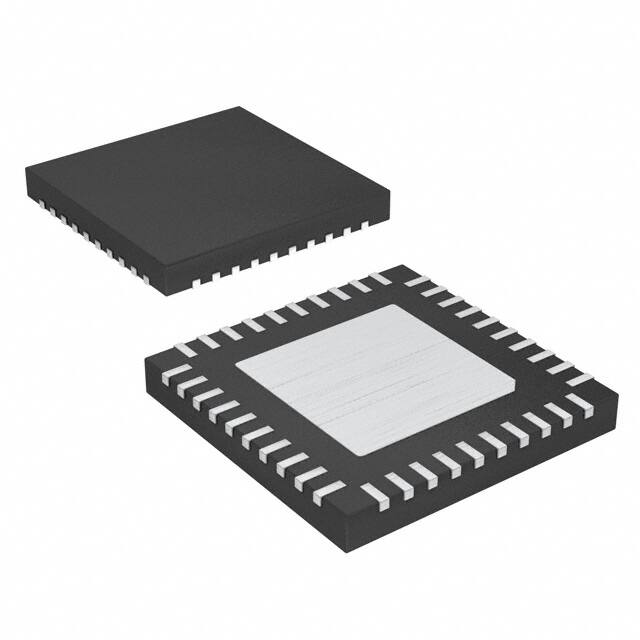


 工商网监
湘ICP备2023018690号
工商网监
湘ICP备2023018690号

