®
ADC700
16-Bit Resolution With Microprocessor Interface
A/D CONVERTER
FEATURES
The clock oscillator is current-controlled for excellent
stability over temperature. Gain and Zero errors may
be externally trimmed to zero. Analog input ranges of
0V to +5V, 0V to +10V, 0V to +20V, ±2.5V, ±5V, and
±10V are available.
● COMPLETE WITH REFERENCE, CLOCK,
8-BIT PORT MICROPROCESSOR
INTERFACE
● CONVERSION TIME: 17µs max
● LINEARITY ERROR: ±0.003% FSR max
● NO MISSING CODES TO 14 BITS OVER
TEMPERATURE
● SPECIFIED AT ±12V AND ±15V SUPPLIES
● OUTPUT BUFFER LATCH FOR IMPROVED
INTERFACE TIMING FLEXIBILITY
● PARALLEL AND SERIAL DATA OUTPUT
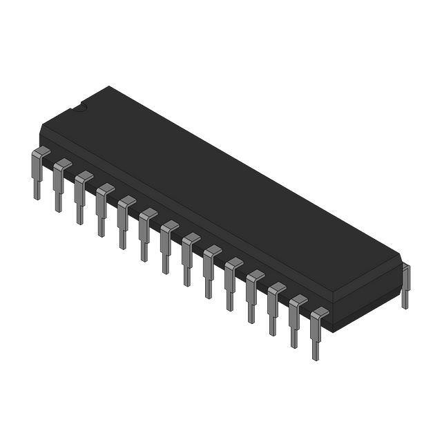
● SMALL PACKAGE: 28-Pin DIP
DESCRIPTION
The ADC700 is a complete 16-bit resolution successive approximation analog-to-digital converter.
The reference circuit, containing a buried zener, is
laser-trimmed for minimum temperature coefficient.
Data
Ready
CS
RD
WR
HBEN
BTCEN
Reset
Status
Serial Data
Strobe
Clock
and
Control Logic
The conversion time is 17µs max for a 16-bit conversion over the three specification temperature ranges.
After a conversion, output data is stored in a latch
separate from the successive approximation logic. This
permits reading data during the next conversion, a
feature that provides flexible interface timing, especially for interrupt-driven interfaces.
Data is available in two 8-bit bytes from TTL-compatible three-state output drivers. Output data is coded in
Straight Binary for unipolar input signals and Bipolar
Offset Binary or Twos complement for bipolar input
signals. BOB or BTC is selected by a logic function
available on one of the pins.
The ADC700 is available in commercial, industrial
and military temperature ranges. It is packaged in a
hermetic 28-pin side-braze ceramic DIP.
Serial Data
Successive
Approximation
Register
16
Comparator
Data
Latch
3State
8
3State
Parallel
Data
10V
Analog
Inputs
20V
SJ
Bipolar
Offset
16-Bit
D/A
Converter
16
Voltage
Reference
International Airport Industrial Park • Mailing Address: PO Box 11400
Tel: (520) 746-1111 • Twx: 910-952-1111 • Cable: BBRCORP •
• Tucson, AZ 85734 • Street Address: 6730 S. Tucson Blvd. • Tucson, AZ 85706
Telex: 066-6491 • FAX: (520) 889-1510 • Immediate Product Info: (800) 548-6132
© 1989 Burr-Brown Corporation
PDS-856A
Printed in U.S.A. October, 1993
�SPECIFICATIONS
ELECTRICAL
At TA = 25°C and at rated supplies: VDD = +5V, +VCC = +12V or +15V, –VCC = –12V or –15V, unless otherwise noted.
ADC700JH,AH,RH
CHARACTERISTICS
MIN
ADC700KH,BH,SH
TYP
MAX
RESOLUTION
MIN
TYP
16
ANALOG INPUTS
Voltage Ranges
Bipolar
Unipolar
Impedance (Direct Input)
0V to +5V, ±2.5V
0V to +10V, ±5V
0V to +20V, ±10V
MAX
UNITS
*
Bits
±2.5, ±5, ±10
0 to +5, 0 to +10, 0 to +20
*
*
V
V
2.5 ±1%
5 ±1%
10 ±1%
*
*
*
kΩ
kΩ
kΩ
DIGITAL SIGNALS (Over Specification Temperature Range)
Inputs
Logic Levels(1)
VIH
+2.0
0
VIL
IIH (VI = +2.7V)
IIL (VI = +0.4V)
Outputs
Logic Levels
VOL (IOL = –1.6mA)
+2.4
VOH (IOH = +20µA)
ILEAKAGE
Data Outputs Only, High Z
+5.5
+0.8
±10
±20
*
*
+0.4
*
*
*
*
V
V
µA
µA
*
V
V
*
10
*
nA
TRANSFER CHARACTERISTICS
ACCURACY
Linearity Error
Differential Linearity Error
Gain Error(3)
Zero Error(3)
Bipolar Zero
Unipolar Zero
Noise at Transitions (3σp-p)
Power Supply Sensitivity
+VCC
–VCC
VDD
DRIFT (Over Specification Temperature Range)
Gain Drift
Zero Drift
Bipolar Zero
Unipolar Zero
Linearity Drift
No Missing Codes Temperature Range
JH (13-bit), KH (14-bit)
AH (13-bit), BH (14 bit)
RH (13-bit), SH (14-bit)
±0.1
±0.05
±0.001
±0.2
±0.1
±0.003
±0.0015
±0.0015
±0.0005
POWER SUPPLY REQUIREMENTS
Voltage Range
+VCC
–VCC
VDD
Current(5)
+VCC
–VCC
VDD
Power Dissipation
TEMPERATURE RANGE
Specification
J, K Grades
A, B Grades
R, S Grades
Storage
*
*
*
% of FSR
% of FSR
% of FSR
%FSR/%VCC
%FSR/%VCC
%FSR/%VDD
*
*
ppm/°C
±5
±2
±1
±10
±4
±3
*
*
*
*
*
±2
ppm of FSR/°C
ppm of FSR/°C
ppm of FSR/°C
*
*
*
°C
°C
°C
+70
+85
+125
*
*
*
17
*
*
*
USB
BTC, BOB
USB, BOB
µs
min
*
*
*
+15
–15
+5
+16
–16
+5.25
+10
–28
+17
645
+15
–35
+20
765
0
–25
–55
–65
+70
+85
+125
+150
®
ADC700
*
*
*
±15
15
+11.4
–11.4
+4.75
% of FSR(2)
% of FSR
%
±8
5
OUTPUT DATA CODES(4)
Unipolar Parallel
Bipolar Parallel(5)
Serial Output (NRZ)
*
±0.003
±0.006
*
*
*
*
0
–25
–55
CONVERSION TIME 16 bits
WARM–UP TIME
±0.1
±0.006
±0.012
±0.2
2
*
*
*
*
*
*
*
*
*
*
*
*
*
VDC
VDC
VDC
*
*
*
*
*
*
*
*
mA
mA
mA
mW
*
*
*
*
°C
°C
°C
°C
�TIMING SPECIFICATIONS(6)
At VDD = +5V, +VCC = +12V or +15V, –VCC = –12V or –15V, unless otherwise noted.
PARAMETER
LIMIT AT
TA = 25°C
LIMIT AT
TA = 0, +70°C
–25°C, +85°C
LIMIT AT
TA = –55°C, +125°C
UNITS
DESCRIPTION
0
130
40
0
17
600
1150
210
360
0
0
145
40
0
17
650
1250
200
400
0
ns, min
ns, max
ns, min
ns, min
µs, max
ns, max
ns, max
ns, min
ns, max
ns, min
CS to WR Setup time
WR to Status delay
WR pulse width
CS to WR Hold time
Conversion time
Data Ready to Status time
WR to first Serial Data Strobe
First Serial Data to first Serial Data Strobe
Last Serial Data Strobe to Status
Status to WR Setup time
0
0
50
0
0
58
0
0
66
ns, min
ns, min
ns, max
70
81
95
ns, max
HBEN to RD Setup time
CS to RD Setup time
High Byte Data Valid after RD
CL = 20pF (High Byte bus access time)
High Byte Data Valid after RD
CL = 100pF (High Byte bus access time)
40
40
50
0
0
40
45
60
0
0
40
50
65
0
0
ns, min
ns, max
ns, max
ns, min
ns, min
RD pulse width
Data Ready delay from RD (HBEN asserted)
Data Hold time after RD (bus relinquish time)
RD to CS Hold time
RD to HBEN Hold time
60
70
70
81
80
95
ns, max
ns, max
Data Ready low delay from Reset
Status low delay from Reset
CONVERSION AND SERIAL DATA OUTPUT TIMING
t1
t2
t3
t4
t5
t6
t7
t8
t9
t10
0
110
40
0
15
550
1100
250
310
0
PARALLEL DATA OUTPUT TIMING
t11
t12
t13 (7)
t14
t15
t16(8)
t17
t18
RESET TIMING
t19
t20
*Same specs as ADC700JH, AH, RH.
NOTES: (1) TTL, LSTTL, and 5V CMOS compatible. (2) FSR means Full Scale Range. For example, unit connected for ±10V range has 20V FSR. (3) Externally
adjustable to zero. (4) See Table I. USB – Unipolar Straight Binary; BTC – Binary Two’s Complement; BOB – Bipolar Offset Binary; NRZ – Non Return to Zero. (5)
Max supply current is specified at rated supply voltages. (6) All input control signals are specified with tRISE = tFALL = 5ns (10% to 90% of 5V) and timed from a voltage
level of 1.6V. (7) t13 is measured with the load circuits of Figure 1 and defined as the time required for an output to cross 0.8V or 2.4V. (8) t16 is defined as the time
required for the data lines to change 0.5V when loaded with the circuits of Figure 2.
ABSOLUTE MAXIMUM RATINGS
PACKAGING INFORMATION
+VDD to Digital Common ............................................................ 0V to +7V
+VCC to Analog Common ......................................................... 0V to +18V
–VCC to Analog Common ......................................................... 0V to –18V
Digital Common to Analog Common ........................................ –1V to +1V
Digital Inputs to Digital Common ................................ –0.5V to VDD + 0.5V
Analog Inputs .................................................................................. +16.5V
Power Dissipation ........................................................................ 1000mW
Storage Temperature ...................................................... –60°C to +150°C
Lead Temperature, (soldering, 10s) ............................................... +300°C
MODEL
ADC700JH
ADC700KH
ADC700AH
ADC700BH
ADC700RH
ADC700SH
PACKAGE
PACKAGE DRAWING
NUMBER(1)
28-Pin Ceramic DIP
28-Pin Ceramic DIP
28-Pin Ceramic DIP
28-Pin Ceramic DIP
28-Pin Ceramic DIP
28-Pin Ceramic DIP
237
237
237
237
237
237
NOTE: (1) For detailed drawing and dimension table, please see end of data
sheet, or Appendix D of Burr-Brown IC Data Book.
NOTES: Stresses above those listed under “Absolute Maximum Ratings”
may cause permanent damage to the device. Exposure to absolute maximum rating conditions for extended periods may affect device reliability.
ORDERING INFORMATION
MODEL
TEMPERATURE
RANGE
LINEARITY
ERROR (%FSR)
ADC700JH
ADC700KH
ADC700AH
ADC700BH
ADC700RH
ADC700SH
0°C to 70°C
0°C to 70°C
–25°C to +85°C
–25°C to +85°C
–55°C to +125°C
–55°C to +125°C
±0.006
±0.003
±0.006
±0.003
±0.006
±0.003
1–24
25–99
100+
®
3
ADC700
�CS
t1
t3
t4
WR
t10
t2
Status
t5
t6
Data Ready
t7
t9
Serial Data Strobe
t8
Serial Data
Start of Conversion and Serial Data Output Timing.
HBEN
t11
t18
t11
CS
t12
t14
t17
t12
t14
t17
RD
t13
Parallel Data
t15
t16
t13
t16
High
Byte
Low
Byte
DB8–DB15
DB0–DB7
Data Ready
ADC700 Parallel Output Timing.
Reset
t19
Data Ready
t20
Status
ADC700 Reset Function Timing Diagram.
The information provided herein is believed to be reliable; however, BURR-BROWN assumes no responsibility for inaccuracies or omissions. BURR-BROWN assumes
no responsibility for the use of this information, and all use of such information shall be entirely at the user’s own risk. Prices and specifications are subject to change
without notice. No patent rights or licenses to any of the circuits described herein are implied or granted to any third party. BURR-BROWN does not authorize or warrant
any BURR-BROWN product for use in life support devices and/or systems.
®
ADC700
4
�PIN CONFIGURATION
5kΩ
Comparator In
Bipolar Offset
2
+VCC
3
Gain Adjust
4
–VCC
5
Reset
6
WR
7
RD
5kΩ
1
8
Voltage
Reference
MSB LSB
Control Logic
LSB
16-Bit
D/A
Converter
28
20V Range
27
10V Range
26
Analog Common
25
Digital Common
24
V DD
23
BTCEN
22
DB15/DB7
21
DB14/DB6
20
DB13/DB5
19
DB12/DB4
18
DB11/DB3
CS
9
HBEN
10
Serial Data
11
Data Ready
12
17
DB10/DB2
Status
13
16
DB9/DB1
Serial Data Strobe
14
15
DB8/DB0
MSB
Successive
Approximation
Register
Data
Latch
3-State
Drivers
Clock and Clock Logic
All internal control lines not shown. Refer to Figures 4 and 5 for Offset and Gain Adjust connections.
DESCRIPTION
AND OPERATING FEATURES
in the buffer register. The Data Ready flag goes low (“0”)
when the most significant byte (high byte) is read. If the
“old” word is not read, or if only the least significant byte
(low byte) is read, Data Ready is not reset. The next
conversion output will overwrite the data latch when the
conversion is complete. The Data Ready flag remains high.
Refer to timing diagrams in the Specifications section.
The ADC700 is a 16-bit resolution successive approximation A/D converter. Parallel digital data as well as serial data
is available. Several features have been included in the
ADC700 making it easier to interface with microprocessors
and/or serial data systems. Several analog input ranges are
available.
SERIAL DATA
Some of the key operating features are described here. More
detail is given in later sections of the data sheet. Refer to the
block diagram above.
Sixteen-bit serial data output is available (pin 11) along with
a serial output strobe (pin 14). This serial data strobe is not
the internal SAR clock but is a special strobe for serial data
consisting of 16 negative-going edges (during conversion)
occurring about 200ns after each serial data bit is valid. This
feature eases the interface to shift registers or through optocouplers for applications requiring galvanic isolation.
RESET
The ADC700 has a Reset input that must be asserted upon
power-up or after a power interruption. This initializes the
SAR, the output buffer register and Data Ready flag. Since
microprocessor systems already use a power-on reset circuit,
the same system reset signal can be used to initialize the
ADC700.
STATUS
The familiar Status (or Busy) flag, present in successive
approximation A/D converters, is available (pin 13) and
indicates that a conversion is in progress. Status is valid
110ns after assertion of the convert command (WR low).
Status cannot be used as a sample-hold control because there
is not enough time for the sample-hold to settle to the
required error band before the ADC700 makes its first
conversion decision.
PARALLEL DATA
The parallel data output is available through an 8-bit port
with 3-state output drivers. High byte and low byte are
selected by HBEN (pin 10).
A buffer/latch is included between the successive approximation register (SAR) and the 3-state drivers. This feature
permits more flexible interface timing than is possible from
most successive approximation converters.
CHIP SELECT
CS (pin 9) selects the ADC700. No other functions can be
implemented unless CS is asserted. WR (pin 7) is the startof-conversion strobe. RD strobes each output data byte,
selected by HBEN (pin 10), to the 3-state drivers.
The “old” word can be read during the next conversion. A
Data Ready flag (pin 12) is asserted when a “new” word is
®
5
ADC700
�TWO’S COMPLEMENT DATA CODE
BTCEN (pin 23) is a logic function that implements the
Binary Two’s Complement output code for bipolar (+ and –)
analog input signal operation. This feature is compatible
with twos complement arithmetic in microprocessor math
algorithms.
Most Significant Bit, MSB
That binary digit that has the greatest value or weight. The
MSB weight is FSR/2.
Resolution
An N-bit binary-coded A/D converter resolves the analog
input into 2N values represented by the 2N digital output
codes.
INTERNAL CLOCK
The ADC700 has a self-contained clock to sequence the
A/D logic. The clock is not available externally. An external
16-pulse strobe (pin 14) is brought out to clock serial data
only. Use of ADC700 with external clock is not possible.
ACCURACY
Linearity Error, Integral Linearity Error (ILE)
Linearity Error is defined as the deviation of actual analog
input values from the ideal values about a straight line drawn
through the code mid-points near positive full scale (at +VFS
–1LSB) and at Zero input (at 1/2LSB below the first code
transition, i.e. at Zero) or, in the case of bipolar operation,
near minus full scale (at 1/2LSB below the first code
transition, i.e. at –VFS). Despite the definition, however,
code transitions are easier to measure than code midpoints.
Therefore linearity is measured as the deviation of the
analog input values from a line drawn between the first and
last code transitions. Linearity Error specifications are expressed in % of Full Scale Range (FSR). ADC700KH ILE
is ±0.003% of FSR which is 1/2 LSB at 14-bits.
INTERNAL VOLTAGE REFERENCE
The ADC700 has an internal low-noise buried-zener voltage
reference. The reference circuit has been drift compensated
over the MIL temperature range using a laser trim algorithm.
The reference voltage is not available externally.
DISCUSSION
OF SPECIFICATIONS
BASIC DEFINITIONS
Differential Linearity Error (DLE), No Missing Codes
Differential Linearity Error is defined as the deviation in
code width from the ideal value of 1LSB. If the DLE is
greater than –1LSB anywhere along the range, the A/D will
have at least one missing code. ADC700KH is specified to
have a DLE of ±0.006% of FSR, which is ±1LSB at 14 bits.
ADC700KH is specified to have no missing codes at the 14bit level over specified temperature ranges.
Refer to Figure 3 for an illustration of A/D converter
terminology and to Table II in the Calibration section.
Full Scale Range, FSR
The nominal range of the A/D converter. For ADC700, the
FSR is 20V for the 0V to +20V and the –10V to +10V input
ranges or 10V for the 0V to +10V and –5V to +5V input
ranges.
Gain Error
The deviation from the ideal magnitude of the input span
between the first code midpoint (at –VFS + 1/2LSB, for
bipolar operation; at Zero for unipolar operation) to the last
code midpoint (VFS –1LSB). As with the linearity error
Least Significant Bit, LSB
The smallest analog input change resolved by the A/D
converter. For an A/D converter with N bits output, the input
value of the LSB is FSR(2–N).
5V
DBN
3kΩ
CL
FFFH
3kΩ
FFDH
CL
DGND
DGND
A) High-Z to VOH (t 3 )
and VOL to VOH (t 6 ).
Gain
Error
Rotates
The
Line
FFEH
Digital Output
DBN
B) High-Z to VOL (t 3 )
and VOH to VOL (t 6 ).
FIGURE 1. Load Circuits for Access Time.
802 H
801 H
800 H
7FFH
7FEH
Offset Error
Shifts The Line
002 H
5V
DBN
DBN
3kΩ
10pF
000 H
10pF
DGND
A) V OH to High-Z.
001 H
3kΩ
1/2LSB
Zero
(–Full
Scale)
DGND
Zero
(–Full-Scale
Calibration
Transition)
Midscale
(Bipolar Zero)
1/2LSB
3/2LSB
+Full-Scale
Calibration
Transition
Analog Input
B) V OL to High-Z.
FIGURE 2. Load Circuits for Output Float Delay.
FIGURE 3. Transfer Characteristic Terminology.
®
ADC700
(Bipolar
Zero
Transition)
6
+Full
Scale
�measurements, code transition values are the locations actually measured for this spec. The ideal gain is VFSR –2LSB.
Gain Error is expressed in % (of reading). See Figure 3.
Gain Error of the ADC700 may be trimmed to zero using
external trim potentiometers.
Power Supply Wiring
Use heavy power supply and power supply common (ground)
wiring. A ground plane is usually the best solution for
preserving dynamic performance and reducing noise coupling into sensitive converter circuits.
Offset Error
Unipolar Offset Error—The deviation of the actual codemidpoint value of the first code from the ideal value located
at 1/2LSB below the ideal first transition value (i.e. at zero
volts).
Bipolar Offset Error—The deviation of the actual codemidpoint of the first code from the ideal value located
at 1/2LSB below the ideal first transition value located at –
VFS +1/2LSB.
Again, transition values are the actual measured parameters.
Offset and Zero errors of the ADC700 may be trimmed to
zero using external trim potentiometers. Offset Error is
expressed as a percentage of FSR.
Bipolar Zero Error—The deviation of the actual midscale-code midpoint value from zero. Transition values are
the actual measured parameter and it is 1/2 LSB below zero
volts. The error is comprised of Bipolar Offset Error, 1/2 the
Gain Error, and the Linearity Error of bit 1. Bipolar Zero
Error is expressed as a percentage of FSR.
When passing converter power through a connector, use
every available spare pin for making power supply return
connections, and use some of the pins as a Faraday shield to
separate the analog and digital common lines.
Power Supply Returns
(Analog Common and Digital Common)
Connect Analog Common and Digital Common together
right at the converter with the ground plane. This will usually
give the best performance. However, it may cause problems
for the system designer. Where it is absolutely necessary to
separate analog and digital power supply returns, each should
be separately returned to the power supply. Do not connect
Analog Common and Digital Common together and then run
a single wire to the power supply. Connect a 1 to 47µF
tantalum capacitor between Digital Common and Analog
Common pins as close to the package as possible.
Power Supply Bypassing
Every power-supply line leading into an A/D converter must
be bypassed to its common pin. The bypass capacitor should
be located as close to the converter package as possible and
tied to a solid ground—connecting the capacitors to a noisy
ground defeats the purpose of the bypass. Use tantalum
capacitors with values of from 10µF to 100µF and parallel
them with smaller ceramic capacitors for high frequency
filtering if necessary.
Power Supply Sensitivity
Power Supply Sensitivity describes the maximum change in
the full-scale transition value from the initial value for a
change in each power supply voltage. PSR is specified in
units of %FSR/% change in each supply voltage.
The major effect of power supply voltage deviations from
the rated values will be a small change in the Gain (scale
factor). Power Supply Sensitivity is also a function of ripple
frequency. Figure 4 illustrates typical Power Supply Sensitivity performance of ADC700 versus ripple frequency.
Separate Analog and Digital Signals
Digital signals entering or leaving the layout should have
minimum length to minimize crosstalk to analog wiring.
Keep analog signals as far away as possible from digital
signals. If they must cross, cross them at right angles.
Coaxial cable may be necessary for analog inputs in some
situations.
INSTALLATION
Shield Other Sensitive Points
The most critical of these is the comparator input (pin 1). If
this pin is not used for offset adjustment, then it should be
surrounded with ground plane or low-impedance power
POWER SUPPLY SELECTION
Linear power supplies are preferred. Switching power supply specifications may appear to indicate low noise output,
but these specifications are rms specs. The spikes generated
in switchers may be hard to filter. Their high-frequency
components may be extremely difficult to keep out of the
power supply return system. If switchers must be used, their
outputs must be carefully filtered and the power supply itself
should be shielded and located as far away as possible from
precision analog circuits.
% FSR/% VS
0.1
LAYOUT CONSIDERATIONS
Because of the high resolution and linearity of the ADC700,
system design problems such as ground path resistance and
contact resistance become very important. For a 16-bit
resolution converter with a +10V Full-Scale Range, 1LSB is
153µV. Circuit situations that cause only second- or thirdorder errors in 8-, 10-, or 12-bit A/D converters can induce
first-order errors in 16-bit resolution devices.
–VCC
0.01
+VCC
+VDD
0.001
1
10
100
1k
10k
100k
Frequency (Hz)
FIGURE 4. Power Supply Rejection Ripple vs Frequency.
®
7
ADC700
�supply plane. If it is used for offset adjustment, the series
resistor and potentiometer should be located as close to the
converter as possible.
consistently done with a fixed series or parallel resistor. The
ADC700 can then be calibrated using the Gain and Offset
adjustments described in the calibration section. For example, using the ±10V input range, one can decrease the
range slightly by paralleling the 10kΩ input resistor (pin 28
to pin 1) with a 610kΩ metal film resistor to achieve a
300µV LSB instead of the nominal standard 305.17578µV
binary LSB.
The Gain Adjust (pin 4) is an input that has a relatively high
input impedance and is susceptible to noise pickup. The
Gain Adjust pin should be bypassed with a 0.01µF to 0.1µF
capacitor whether or not the gain adjust feature is used.
If the 20V Analog input range is used (pin 28), the 10V
Range input (pin 27) may need to be shielded with ground
plane to reduce noise pickup.
OPTIONAL EXTERNAL GAIN AND OFFSET TRIM
Gain and Offset Error may be trimmed to zero using external
Gain and Offset trim potentiometers connected to the
ADC700 as shown in Figures 6 and Figure 7. A calibration
procedure in described in the Operating Instructions section.
ANALOG SIGNAL SOURCE IMPEDANCE
The input impedance of the ADC700, typical of most successive approximation A/D converters, is relatively low
(2.5kΩ to 10kΩ). The input current of a successive
approximation A/D converter changes rapidly during the
conversion algorithm as each bit current is compared to the
analog input current. Since the output impedance of a
closed-loop amplifier or a sample-hold amplifier increases
with frequency and, in addition, the amplifier must settle to
the required accuracy in time for the next comparison/
decision after such a disturbance, care must be taken to
select the proper driving amplifier.
Multiturn potentiometers with 100ppm/°C or better TCR are
recommended for minimum drift over temperature. These
potentiometers may be any value from 10kΩ to 100kΩ. All
resistors should be 20% carbon or better. Pin 1 (Comparator
In) and pin 4 (Gain Adjust) may be left open if no external
adjustment is planned; however, pin 4 should always be
bypassed with 0.01µF or larger to Analog Common.
OPERATING INSTRUCTIONS
Unfortunately, high-accuracy operational amplifiers tend to
have low bandwidth, while wide-band amplifiers tend to
have lower accuracy. One solution is to use a wide-band but
perhaps less precise amplifier. Another solution is to add a
wide-band buffer amplifier such as the Burr-Brown OPA633
inside the feedback loop of a slower (but precision) amplifier, Figure 5. This reduces the output impedance at high
frequencies yet preserves the accuracy at low frequencies.
When a sample/hold is needed, a high-linearity, high-speed
sample/hold such as the Burr-Brown SHC76 should be used
to drive the ADC700.
CALIBRATION
Offset and Gain may be trimmed by external Offset and
Gain potentiometers. Offset is adjusted first and then Gain.
Calibration values are listed in Table II for all ADC700
input ranges. Offset and Gain calibration can be accomplished to a precision of about ±1/2LSB using a static
adjustment procedure described below. By summing a small
sine or triangular wave voltage with the accurate calibration
voltage applied to the analog input, the output can be swept
through each of the calibration codes to more accurately
determine the transition points listed in Table II. NOTE: The
transition points are not the same as the code midpoints used
in the static calibration example.
ANALOG INPUT RANGES
The analog input circuits of the ADC700 can be connected
to accept unipolar or bipolar input signals. These ranges and
connections are tabulated in Table I. Circuit connections are
shown in Figures 6 and 7. Gain and offset adjustments are
described in the calibration section.
OFFSET ADJUSTMENT,
14-BIT RESOLUTION EXAMPLE
Static Adjustment Procedure (At Code Midpoints)
0V to +10V Range—Set the analog input to +1LSB14 =
0.00061V. Adjust the Offset potentiometer for a digital
output of 0004H. Set the analog input to +Full Scale –
2LSB14 = +9.9987V. Adjust the Gain potentiometer for a
digital output of FFFCH. For a half-scale calibration check,
set the analog input to +5.0000V and read a digital output
code of 8000H.
To operate the ADC700 with a range that gives other
convenient values for the LSB, the input resistor may be
increased or decreased slightly without seriously affecting
the Gain Drift of the converter. Since the input resistors of
the ADC700 are within ±2% from unit to unit, this can be
Precision
Low Bandwidth
Op Amp
INPUT
SIGNAL
RANGE
Wideband
Buffer
±10V
±5V
±2.5V
0V to +5V
0V to +10V
0V to +20V
A/D
Converter
OPA111
OPA27
OPA633
Analog
Common
FIGURE 5. Wideband Buffer Reduces Output Impedance at
High Frequencies.
BTCEN = 0
BOB
BOB
BOB
USB
USB
USB
BTC
BTC
BTC
—
—
—
1
1
1
26
26
26
CONNECT
PIN 28
TO PIN
CONNECT
SIGNAL
TO PIN
Input Signal
Open
Pin 1
Pin 1
Open
Input Signal
28
27
27
27
27
28
TABLE I. ADC700 Input Range Connections.
®
ADC700
BTCEN = 1
CONNECT
PIN 2
TO PIN
OUTPUT CODE
8
�VOLTAGE (V)
ANALOG INPUT
RANGE
±10
±5
±2.5
0 TO +20
0 TO +10
0 TO +5
+VFS
–VFS
FSR
+10
–10
20
+5
–5
10
+2.5
–2.5
5
+20
0
20
+10
0
10
+5
0
5
TRANSITION CODES
(Hexadecimal)
TRANSITION VALUES (V)
For 16-bit Resolution (Reading all 16 bits)
FFFEH to FFFFH
7FFFH to 8000H
0000H to 0001H
LSB (FSR/216)
+9.999542
–152.5µV
–9.999847
305µV
+4.999771
–38µV
–4.999924
153µV
+2.499886
–19µV
–2.499962
38µV
+19.999542
+9.999847
+152µV
305µV
+9.99971
+4.999924
+76µV
153µV
+4.999886
+2.499962
+38µV
76µV
+2.499771
–76µV
–2.499924
153µV
+19.999084
+9.999625
+305µV
610µV
+9.999542
+4.999847
+152µV
305µV
+4.999771
+2.499924
+76µV
153µV
+2.49954
–153µV
–2.499847
305µV
+19.99817
+9.99939
+610µV
1221µV
+9.99908
+4.999695
+305µV
610µV
+4.99954
+2.499847
+153µV
305µV
For 15-bit Resolution (Reading all 16 bits, Ignoring DB0)
FFFDH to 7FFEH
7FFEH to 8000H
0000H to 0002H
LSB (FSR/215)
+9.999084
–305µV
–9.999695
610µV
+4.999542
–153µV
–4.999847
305µV
For 14-bit Resolution (Reading all 16 bits, Ignoring DB0 and DB1)
FFFCH to FFFDH
7FFDH to 8000H
0000H to 0004H
LSB (FSR/214)
+9.99817
–610µV
–9.999390
1221µV
+4.99908
–305µV
–4.999694
610µV
TABLE II. Transition Values for Calibration.
+VCC
Potentiometers
10kΩ to 100kΩ
270kΩ
4
Gain Adjust
R1
–VCC
10V Range
27
Comparator
0.01µF
28
+VCC
20V Range
1
Comparator Input
R2
1.8MΩ
Analog
Input
2
–VCC
BPO
26
Analog Common
FIGURE 6. Unipolar Input Configuration with Gain and Offset Adjust Connections.
+VCC
Potentiometers
10kΩ to 100kΩ
270kΩ
4
Gain Adjust
R1
–VCC
10V Range
27
Comparator
0.01µF
28
+VCC
20V Range
1
Comparator Input
R2
1.8MΩ
Analog
Input
2
–VCC
BPO
26
Analog Common
FIGURE 7. Bipolar Input Configuration with Gain and Offset Adjust Connections.
®
9
ADC700
�START OF CONVERSION
A conversion is started by asserting CS and WR Low. Status
goes high about t = t1 + t2 = 110ns later. The first successive
approximation decision occurs about 900ns after WR is
asserted. Status goes Low after the conversion is complete.
Refer to Start of Conversion and Serial Data Output Timing
following the Timing Specifications Table.
–10V to +10V Range—Set the analog input to –FS +
1LSB14 = –9.99878V. Adjust the Offset potentiometer for a
digital output of 0004H (8004H if BTCEN is asserted). Set
the analog input to +9.9976V. Adjust the Gain potentiometer
for a digital output of FFFCH (7FFCH if BTCEN is assrted).
For a half-scale calibration check, set the analog input to
0.0000V and read a digital output code of 8000H (0000H if
BTCEN is asserted).
DATA READY FLAG
CONTROLLING AND
INTERFACING THE ADC700
The data latch feature permits data to be read during the
following conversion. The Data Ready flag indicates that the
data from the most recent conversion is latched in the output
data latch and that it hasn’t been read. Data Ready remains
High until the most significant data byte is read. If a
subsequent conversion is initiated and completed, the new
word will be stored in the output data latch regardless of the
state of the Data Ready flag. The preceding word will be
overwritten and lost.
RESET
The ADC700 requires a Reset command upon power-up or
after a power interruption to guarantee the condition of
internal registers. If Status powers-up High, no conversion
can be started. Reset initializes the SAR, the output buffer
register, and the Data Ready flag and terminates a conversion in progress. Since microprocessor systems already use
a power-on reset circuit, the same system reset signal can be
used to initialize the ADC700. A power-up circuit is shown
in Figure 8. Refer to Reset function timing diagram following the Timing Specifications Table.
READING PARALLEL DATA
Parallel data is latched in the output data latch at the end of
a conversion. Data can be read any time, even during the
subsequent conversion. The output data latch is not cleared
by reading the data. Only the Data Ready flag is cleared by
reading the MSB.
+5V
The output three-state drivers are enabled by asserting the
CS and RD inputs Low. When HBEN is Low, the most
significant eight bits are enabled and the Data Ready flag is
cleared. When HBEN is High, the least significant eight bits
are enabled. Refer to Parallel Data Output Timing information following the Timing Specifications Table.
24
V DD
50kΩ
6
Reset
100pF
To reduce noise interference to the absolute minimum, data
should be read after the current conversion is complete.
However, data can be read during the following conversion,
with minimal interference, to maximize the sampling rate of
the converter.
ADC700
FIGURE 8. Power-Up Reset Circuit.
A typical parallel interface is illustrated in Figure 9.
READING SERIAL DATA
A 0–A XX
Microprocessor
Address
Decoder
Serial data output of the ADC700 is facilitated by a Serial
Data Strobe that provides 16 negative-going edges for strobing
an external serial to parallel shift register located perhaps on
the other side of an opto-coupler. Refer to the Serial Data
Timing information following the Timing Specifications
Table. An example of an isolation connection using the
serial port feature is illustrated in Figure 10.
ADC700
CS
WR
WR
RD
RD
INT
Data Ready
Reset
Reset
CONTINUOUS CONVERSION OPERATION
DB 0 –DB 7
When CS is permanently connected to Digital Common and
Status is connected to WR, Figure 11, the ADC700 will
continuously convert. The repetition time will not be precise
and will vary slightly with the temperature for the ADC700
because the time will be determined by the internal clock
frequency and control-circuit gate delays. If a precise repetition rate is needed, the continuous conversion connection
should not be used.
DB 0 –DB 7
System Reset
FIGURE 9. Parallel Data Bus Interface.
®
ADC700
10
�ADC700
CS
Serial
Data
WR
V DD
ADC700
V DD
To Interrupt
Status
Serial
Data
Strobe
FIGURE 11. Continuous Conversion Circuit Connection.
Reset
Isolation Barrier
FIGURE 10. Serial Data Output Providing Convenient
Isolation.
PIN DESIGNATION
DEFINITION
FUNCTION
CS (Pin 9)
WR (Pin 7)
RD (Pin 8)
HBEN (Pin 10)
Must be Low to either initiate a conversion or read output data.
Conversion begins after the High-to-Low transition.
Turns ON the three-state output drivers upon being asserted low.
Selects the MSB or the LSB for readout. Data Ready is cleared when HBEN is Low and RD is asserted.
Reset (Pin 6)
Chip Select
Write (Convert)
Read
High Byte Enable
“1” = Low Byte
“0” = High Byte
Reset
BTCEN (Pin 23)
BTC Enable
Resets internal logic. Must be asserted after power-up or a power interruption clears Status and Data
Ready to Low.
Sets the output code to Binary Twos Complement (BTC) when Low. Output code is Bipolar Offset Binary
(BOB) when High.
TABLE III. Control Line Functions.
CONTROL LINE
RESET
WR
RD
HBEN
CS
0
1
1
1
1
1
1
X
X
0
1
1
0
0
X
X
X
0
0
0
0
X
X
X
0
1
0
1
X
1
0
0
0
0
0
OPERATION
Reset converter logic. Status and Data Ready set Low.
No operation.
Initiate conversion.
Places High Byte on output port. Clears Data Ready flag.
Placed Low Byte on output port. Does not clear Data Ready flag.
Initiates conversion and places High Byte or output port. Clears Data Ready.
Initiates conversion and places Low Byte on output port. Does not clear Data Ready flag.
NOTE: If a conversion command is asserted while a conversion is in progress, the command is ignored. If the conversion command remains asserted when a
conversion is finished, a new conversion will begin.
TABLE IV. Control Input Truth Table.
®
11
ADC700
�Because the last data-word is stored in the data latch, it is
possible to read it during the next A/D conversion. Assertion
of CS and HBEN for reading parallel data should be timed
from Status going low. The two-byte read operation must be
complete before the conversion in process is complete or the
Data Read is invalid.
Analog
In
SHC76
ADC700
Mode
Control
Serial Data is available during continuous conversion with
word synchronization available from STATUS.
Sample
Mode
Control
USING A SAMPLE/HOLD WITH ADC700
Figure 12 illustrates using ADC700 with the Burr-Brown
SHC76. The sample-to-hold settling time (to 14 bits,
±0.003%FSR) of the SHC76 is 1µs typ, 3µs max. The time
from the Status going High to the first conversion decision
is about 900ns. Therefore a time delay between the Sampleto-Hold command to the WR command to the ADC700 is
required.
1µs to 3µs
ADC700
WR
Start Conversion
FIGURE 12. Using Sample/Hold with ADC700 Requires
Time Delay Between Sample and Start-of-Conversion.
®
ADC700
Hold
12
�


 工商网监
湘ICP备2023018690号
工商网监
湘ICP备2023018690号
