User's Guide
SBAU200C – June 2012 – Revised April 2020
Performance Demonstration Kit for the ADS131E08
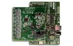
Figure 1. ADS131E08EVM-PDK
This user's guide describes the characteristics, operation, and use of the ADS131E08EVM-PDK. This
performance demonstration kit is an evaluation module for the ADS131E08, an eight-channel, 24-bit, lowpower, integrated analog front-end (AFE) designed for power protection circuits. The ADS131E08EVMPDK is intended for prototyping and evaluation. This user's guide includes a complete circuit description,
schematic diagram, and bill of materials.
Throughout this document, the terms ADS131E08EVM-PDK, demonstration kit, evaluation board,
evaluation module, and EVM are synonymous with the ADS131E08EVM.
The following related documents are available through the Texas Instruments web site at www.ti.com.
Table 1. Related Documentation
1
2
3
Device
Literature Number
ADS131E08
SBAS561
Contents
ADS131E08EVM Overview................................................................................................. 3
Software Installation ......................................................................................................... 5
ADS131E08EVM Daughter-Card Hardware Overview ................................................................ 10
SBAU200C – June 2012 – Revised April 2020
Submit Documentation Feedback
Performance Demonstration Kit for the ADS131E08
Copyright © 2012–2020, Texas Instruments Incorporated
1
�www.ti.com
4
5
6
Using the Software ......................................................................................................... 14
ADS131E08 Analysis Tools ............................................................................................... 22
Bill of Materials (BOM), Layout, and Schematic ....................................................................... 28
List of Figures
1
ADS131E08EVM-PDK ...................................................................................................... 1
2
ADS131E08EVM-PDK Kit .................................................................................................. 4
3
Initialization of ADS131E08EVM GUI ..................................................................................... 6
4
License 1...................................................................................................................... 6
5
License 2...................................................................................................................... 6
6
New Hardware Wizard Screen 1
7
New Hardware Wizard Screen 2
8
9
10
11
12
13
14
15
16
17
18
19
20
21
22
23
24
25
26
27
28
29
30
31
.......................................................................................... 7
.......................................................................................... 7
New Hardware Wizard Screen 3 .......................................................................................... 8
Completion of the First USB Driver........................................................................................ 8
Second New Hardware Wizard Screen ................................................................................... 9
Installing the USBStyx Driver .............................................................................................. 9
File Save Option Under Save Tab ....................................................................................... 14
Channel Registers GUI for the Configuration Registers .............................................................. 15
Channel Control Register GUI Panel: Single Channel Enabled ..................................................... 16
Channel Control Registers GUI Panel: All Channels Enabled ....................................................... 16
Example of Internal Test Signals Viewed on the Scope Display Tab ............................................... 17
Internal Temperature Sensor ............................................................................................. 18
Eight-Channel Read of Internal Temperature Data .................................................................... 18
GPIO Control Register GUI Panel ....................................................................................... 19
Fault Status Indicator ...................................................................................................... 20
Device Register Settings .................................................................................................. 21
Scope Tool Features....................................................................................................... 22
Scope Analysis Tab (Noise Levels for Each Channel Shown) ....................................................... 23
Zoom Option on the Waveform Examination Tool ..................................................................... 23
Histogram Bins ............................................................................................................. 24
Statistics for the Signal Amplitude of Eight Channels ................................................................. 24
Analysis→FFT Graph of Normal Electrode Configuration ............................................................ 25
Analysis→FFT→AC Analysis Parameters: Windowing Options ..................................................... 26
Analysis→FFT→FFT Analysis: Input Short Condition ................................................................ 26
Changing the User-Defined Dynamic Range for Channel 1 .......................................................... 27
FFT Plot Using Waveform Zoom Function .............................................................................. 27
List of Tables
2
1
Related Documentation ..................................................................................................... 1
2
Power-Supply Test Points................................................................................................. 10
3
Analog Supply Configurations ............................................................................................ 11
4
Digital Supply Configurations (DVDD and DGND) ..................................................................... 11
5
CLK Jumper Options....................................................................................................... 12
6
External Reference Jumper Options ..................................................................................... 12
7
Auxiliary Connector Test Signals and Test Points ..................................................................... 12
8
Serial Interface Pinout ..................................................................................................... 13
9
Register Assignments: Channel-Specific Settings ..................................................................... 16
10
GPIO: General-Purpose I/O Register.................................................................................... 19
11
ADS131E08 Bill of Materials
.............................................................................................
Performance Demonstration Kit for the ADS131E08
Copyright © 2012–2020, Texas Instruments Incorporated
28
SBAU200C – June 2012 – Revised April 2020
Submit Documentation Feedback
�ADS131E08EVM Overview
www.ti.com
Trademarks
Pentium III, Celeron are registered trademarks of Intel Corporation.
Microsoft, Windows are registered trademarks of Microsoft Corporation.
SPI is a trademark of Motorola, Inc..
All other trademarks are the property of their respective owners.
1
ADS131E08EVM Overview
1.1
Information about Cautions
This document contains caution statements. The information in a caution statement is provided for your
protection. Be sure to read each caution carefully.
CAUTION
This is an example of a caution statement. A caution statement describes a
situation that could potentially damage your software or equipment.
1.2
Introduction
The ADS131E08EVM-PDK is intended for evaluating the ADS131E08 low-power, 24-bit, simultaneouslysampling, eight-channel analog-to-digital converter (ADC). The digital SPI™ control interface is provided
by the MMB0 modular EVM motherboard that connects to the ADS131E08 evaluation board. The
ADS131E08EVM-PDK is designed to expedite evaluation and system development.
The MMB0 motherboard allows the ADS131E08EVM to be connected to the computer thorugh an
available USB port. This manual shows how to use the MMB0 as part of the ADS131E08EVM-PDK, but
does not provide technical details about the MMB0.
1.3
Supported Features
Hardware Features:
• Configurable for bipolar or unipolar supply operation
• Configurable for internal and external clock through jumper settings
• Analog test signals can be applied easily using screw terminals
Software Features:
• Analysis tools, including a virtual oscilloscope, histogram, and fast Fourier transform (FFT)
• Access to a variety of register contents, including data rate, PGA options, and more.
• Set ADS131E08 register settings with easy-to-use, graphical user interface (GUI) software
1.3.1
Features Not Supported in Current Version
32 kSPS and 64 kSPS data capture is not supported by the current version of the firmware.
SBAU200C – June 2012 – Revised April 2020
Submit Documentation Feedback
Performance Demonstration Kit for the ADS131E08
Copyright © 2012–2020, Texas Instruments Incorporated
3
�ADS131E08EVM Overview
1.4
www.ti.com
ADS131E08EVM Hardware
Figure 2 shows the hardware included in the ADS131E08EVM kit. Contact the factory at http://e2e.ti.com
if any component is missing. Also, it is highly recommended that you check the TI website at
http://www.ti.com to verify that you have the latest software.
Figure 2. ADS131E08EVM-PDK Kit
The complete kit includes the following items:
• ADS131E08EVM printed-circuit board (PCB)
• MMB0 (modular EVM motherboard)
An external power supply is required to power the MMB0 board. Any supply used to power the MMB0
board through the jack located at J2 must comply with the following requirements:
• Output voltage: 5.5 VDC to 15 VDC
• Maximum output current: ≥ 500 mA
• Output connector: barrel plug (positive center), 2.5-mm I.D. x 5.5-mm O.D. (9-mm insertion depth)
• Complies with applicable regional safety standards
4
Performance Demonstration Kit for the ADS131E08
Copyright © 2012–2020, Texas Instruments Incorporated
SBAU200C – June 2012 – Revised April 2020
Submit Documentation Feedback
�Software Installation
www.ti.com
2
Software Installation
2.1
Minimum Requirements
Before installing the software that is intended for use with the EVM kit, please verify that your PCcompatible computer meets the following minimum requirements:
• Pentium III® or Celeron® processor, 866 MHz or equivalent
• Minimum 256 MB of RAM (512 MB or greater recommended)
• USB 1.1-compatible input
• Hard disk drive with at least 200 MB free space
• Microsoft® Windows® XP operating system with SP2, or Windows 7 operating system
• Mouse or other pointing device
• 1280 × 960 minimum display resolution
SBAU200C – June 2012 – Revised April 2020
Submit Documentation Feedback
Performance Demonstration Kit for the ADS131E08
Copyright © 2012–2020, Texas Instruments Incorporated
5
�Software Installation
2.2
www.ti.com
Installing the Software
CAUTION
Do not connect the ADS131E08EVM hardware before installing the software on
a suitable PC. Failure to observe this caution may cause Microsoft Windows to
not recognize the ADS131E08EVM.
Download the latest software from the TI website at www.ti.com/tool/ADS131E08EVM-PDK. To install the
ADS131E08 software, unzip and run setup.exe. Figure 3 shows the initialization screen.
Figure 3. Initialization of ADS131E08EVM GUI
You must accept the two license agreements shown in Figure 4 and Figure 5 before the installation can
proceed.
Figure 4. License 1
6
Performance Demonstration Kit for the ADS131E08
Copyright © 2012–2020, Texas Instruments Incorporated
Figure 5. License 2
SBAU200C – June 2012 – Revised April 2020
Submit Documentation Feedback
�Software Installation
www.ti.com
2.3
2.3.1
Installing the ADS131E08EVM-PDK Hardware Drivers
Installing the First USB Driver
Apply power to the MMB0 using a power supply as discussed in Section 1.4 and connect the MMB0 to
your PC through any available USB port. The Found New Hardware Wizard window appears, as shown in
Figure 6. Note that this is the first of two USB drivers that are installed. Click Next to continue driver
installation.
Figure 6. New Hardware Wizard Screen 1
Click Next when the screen in Figure 7 appears.
Figure 7. New Hardware Wizard Screen 2
SBAU200C – June 2012 – Revised April 2020
Submit Documentation Feedback
Performance Demonstration Kit for the ADS131E08
Copyright © 2012–2020, Texas Instruments Incorporated
7
�Software Installation
www.ti.com
Navigate to C:\Program Files\ADS131E08EVM\USB Driver, as shown in Figure 8.
Figure 8. New Hardware Wizard Screen 3
Click Next to find and install the driver. When the wizard is complete, the screen in Figure 9 appears.
Figure 9. Completion of the First USB Driver
8
Performance Demonstration Kit for the ADS131E08
Copyright © 2012–2020, Texas Instruments Incorporated
SBAU200C – June 2012 – Revised April 2020
Submit Documentation Feedback
�Software Installation
www.ti.com
2.3.2
Installing the Second USB Driver
Launch the ADS131E08EVM-PDK software from the program menu. The software loads and begins
downloading firmware to the processor on the MMB0. After the firmware is loaded and running, the Found
New Hardware Wizard starts again, as shown in Figure 10.
Figure 10. Second New Hardware Wizard Screen
Click Next and the screen in Figure 11 appears.
Figure 11. Installing the USBStyx Driver
Click Next to complete the installation. If the computer is unable to find the USBStyx driver, point to the
installation directory of C:\Program Files\ADS131E08EVM\USB Drivers.
At this time, you may receive an error message because the ADS131E08EVM-PDK software has timed
out. If so, click OK, close the GUI program, power cycle the ADS131E08EVM, and restart the newly
installed ADS131E08 evaluation program. This process may need to be repeated if you plug the
ADS131E08EVM-PDK into a different USB port on your computer.
SBAU200C – June 2012 – Revised April 2020
Submit Documentation Feedback
Performance Demonstration Kit for the ADS131E08
Copyright © 2012–2020, Texas Instruments Incorporated
9
�ADS131E08EVM Daughter-Card Hardware Overview
3
www.ti.com
ADS131E08EVM Daughter-Card Hardware Overview
CAUTION
Many of the components on the ADS131E08EVM are susceptible to damage
by electrostatic discharge (ESD). Customers are advised to observe proper
ESD handling procedures when unpacking and handling the EVM, including the
use of a grounded wrist strap, bootstraps, or mats at an approved ESD
workstation. An electrostatic smock and safety glasses should also be worn.
The ADS131E08EVM-PDK board is a four-layer circuit board. The board layout and schematics are
appended to the end of this document.
The ADS131E08EVM-PDK is configured to be used with the TI MMB0 data converter evaluation platform.
The key features of the ADS131E08 system on a chip (SOC) are:
• Eight integrated instrumentation amplifiers (INAs) and eight, 24-bit, high-resolution ADCs
• Low power consumption
• Data rates of 1 kSPS, 2 kSPS, 4 kSPS, 8 kSPS, 16 kSPS, 32 kSPS, and 64 kSPS (NOTE: 32 kSPS
and 64 kSPS data capture is not supported by the current version of the firmware).
• 3-V to 5-V unipolar or bipolar analog supply, and 1.8-V to 3-V digital supply
• SPI data interface
The following sections explain some of the hardware settings possible with the EVM for evaluating the
ADS131E08 under various test conditions.
3.1
Power Supply
The ADS131E08EVM mounts on the MMB0 board with connectors J1, J2, and J3. The main power
supplies (+5 V, +3 V, and +1.8 V) for the front-end board are supplied by the host MMB0 board through
connector J3. All other power supplies required for the front-end board are generated onboard by power
management devices.
The ADS131E08 operates in unipolar mode using a +3.0-V to +5.0-V analog supply (AVDD/AVSS) and a
+1.8-V to +3.3-V digital supply (DVDD), or in bipolar mode using the onboard analog supply (±1.5 V to
±2.5 V). The power consumption of the front-end board is measured by using the JP3 jumper. Power
down the ADS131E08 by shorting jumper JP4.
Test points TP4, TP5, TP6, TP7, TP8, TP9, TP10, and TP13 are provided to verify that the host power
supplies are correct. The corresponding voltages are shown in Table 2.
Table 2. Power-Supply Test Points
Test Point
10
Voltage
TP7
+5.0 V
TP4
–4.96 V
TP9
+1.8 V
TP10
+3.3 V
TP5
+3.0 V
TP13
+2.5 V
TP6
–2.5 V
TP8
GND
Performance Demonstration Kit for the ADS131E08
Copyright © 2012–2020, Texas Instruments Incorporated
SBAU200C – June 2012 – Revised April 2020
Submit Documentation Feedback
�ADS131E08EVM Daughter-Card Hardware Overview
www.ti.com
The front-end board must be properly configured in order to achieve the various power-supply schemes.
The default power-supply setting for the ADS131E08EVM is a bipolar analog supply of ±2.5 V, and there
are onboard options to switch to a unipolar analog supply of +3 V. The digital supply (DVDD) is selectable
to either +3.3 V or +1.8 V. Table 3 shows the board and component configurations for each analog powersupply scheme. Table 4 shows the board configurations for the digital supply. Note that the EVM is
shipped with the analog supply set to ±2.5 V and digital supplies set to 3.3 V.
Table 3. Analog Supply Configurations
Unipolar Analog Supply
Bipolar Analog Supply
AVDD and AVSS
3V
5V
±1.5 V
±2.5 V
JP7
1-2
1-2
2-3
2-3
JP1
2-3
2-3
1-2
1-2
U6
TPS73230
TPS73250
Don't care
Don't care
U8
Don't care
Don't care
TPS73201
TPS73201
U7
Don't care
Don't care
TPS72301
TPS72301
R61
Don't care
Don't care
21 kΩ
47.5 kΩ
R62
Don't care
Don't care
78.7 kΩ
43.2 kΩ
R59
Don't care
Don't care
23.3 kΩ
49.9 kΩ
R60
Don't care
Don't care
95.3 kΩ
46.4 kΩ
C48, C54, C59
Not installed
Not installed
Not installed
Not installed
Table 4. Digital Supply Configurations (DVDD and
DGND)
DVDD
3.3 V
1.8 V
JP11
2-3
1-2
SBAU200C – June 2012 – Revised April 2020
Submit Documentation Feedback
Performance Demonstration Kit for the ADS131E08
Copyright © 2012–2020, Texas Instruments Incorporated
11
�ADS131E08EVM Daughter-Card Hardware Overview
3.2
www.ti.com
Clock
The ADS131E08 has an on-chip oscillator circuit that generates a 2.048-MHz clock (nominal). This clock
can vary by ±5% over temperature. For applications that require higher accuracy, the ADS131E08 can
also accept an external clock signal. The ADS131E08 provides an option to test both internal and external
clock configurations. It also provides an option to generate the external clock from either the onboard
oscillator or from an external clock source.
The onboard oscillator is powered by the DVDD supply of the ADS131E08. Care must be taken to ensure
that the external oscillator can operate either with +1.8 V or +3.3 V, depending on the DVDD supply
configuration. Table 5 shows the jumper settings for the three options for the ADS131E08 clocks.
Table 5. CLK Jumper Options
ADS131E08 Clock
Internal Clock
External OSC Clock
JP5
Not installed
2-3
External Clock
1-2
JP6
Don't care
1-2 (disable)
Don't care
J4 - pin 10
Don't care
Don't care
Clock source
A 2.048-MHz oscillator available for the +3.3-V DVDD supply is the FXO-HC735-2.048MHz. For a +1.8-V
DVDD supply, use the SiT8002AC-34-18E-2.048. The EVM is shipped with the external oscillator enabled.
3.3
Reference
The ADS131E08 has an on-chip internal reference circuit that provides reference voltages to the device.
Alternatively, the internal reference can be powered down and VREFP can be applied externally. This
configuration is achieved with the external reference generators (U2 and U3) and driver buffer. These
components (U2, U3, and U4) must be installed by the user; they are not installed at the factory. The
external reference voltage can be set to either 4.096 V or 2.5 V, depending on the analog supply voltage.
Measure TP3 to make sure the external reference is correct and stable. The settings for the external
reference is described in Table 6. This table assumes REF5025 is installed at U2 and REF5040 at U3. A
low-noise amplifier like the OPA350 can be installed at U4.
Table 6. External Reference Jumper Options
Internal Reference
3.3.1
External Reference
ADS131E08 Reference
VREF = 2.5 V
VREF = 4.096 V
VREF = 2.5 V
JP12
Don't care
2-3
1-2
JP2
Not installed
Installed
Installed
Accessing ADS131E08 Analog Supplies
Some ADS131E08 output signals are provided as test points for probing purposes using J4 (not installed
on the board). Table 7 lists the various test signals with the corresponding test points.
Table 7. Auxiliary Connector Test Signals and Test Points
Signal
12
J4 Pin Number
Signal
Not connected
1
2
GPIO1
Not connected
3
4
GPIO2
GPIO3
PWDN
5
6
Dasiy in
7
8
GPIO4
AGND
9
10
Not connected
Performance Demonstration Kit for the ADS131E08
Copyright © 2012–2020, Texas Instruments Incorporated
SBAU200C – June 2012 – Revised April 2020
Submit Documentation Feedback
�ADS131E08EVM Daughter-Card Hardware Overview
www.ti.com
3.3.2
Accessing ADS131E08 Digital Supplies
The ADS131E08 digital signals (including SPI signals, some GPIO signals, and some control signals) are
available at connector J1. These signals are used to interface to the MMB0 board DSP. The pinout for this
connector is shown in Table 8.
Table 8. Serial Interface Pinout
Signal
3.4
J1 Pin Number
Signal
START/CS
1
2
CLK
3
4
CLKSEL
GND
NC
5
6
GPIO1
RESET
CS
7
8
NC
9
10
GND
DIN
11
12
GPIO2
DOUT
13
14
NC/START
DRDY
15
16
SCL
EXT_CLK
17
18
GND
NC
19
20
SDA
Analog Inputs
The ADS131E08 provides users the option to feed in signals from any arbitrary signal source directly.
Analog signals can be applied at terminal blocks J5 through J12.
SBAU200C – June 2012 – Revised April 2020
Submit Documentation Feedback
Performance Demonstration Kit for the ADS131E08
Copyright © 2012–2020, Texas Instruments Incorporated
13
�Using the Software
4
www.ti.com
Using the Software
The software GUI contains a Save to File feature (located in the Save tab) that allows all data from any
combination of channels, along with notes to describe the data, to be saved to a specified directory. This
data can then be read back using a text editor. Saving the data in this format can be completed by clicking
the Save to File button, as shown in Figure 12.
An additional option in the evaluation software allows register configurations to be saved to a file that can
be reloaded to the GUI. To create a configuration file with all of the stored register settings, use the Save
Configuration Settings option, found in the File menu at the top left-hand corner of the GUI. This
configuration file can be reloaded to the GUI using the Load Configuration Settings option found in the
same File menu.
Figure 12 shows the options available in the Save tab.
Figure 12. File Save Option Under Save Tab
14
Performance Demonstration Kit for the ADS131E08
Copyright © 2012–2020, Texas Instruments Incorporated
SBAU200C – June 2012 – Revised April 2020
Submit Documentation Feedback
�Using the Software
www.ti.com
4.1
Software Overview
This section provides a quick overview of the various features and functions of the ADS131E08EVM
software package.
There are four tabs across the left side of the GUI; from top to bottom, they are:
• About: Provides information about the EVM and software version revisions.
• ADC Register: Includes all of the control registers for the ADS131E08 in a series of related subtabs:
– Channel Registers
– GPIO
– Register Map
• Analysis: Provides different ways to analyze captured data, in the time or frequency domain, using the
following subtabs:
– Scope
– Histogram
– FFT
• Save: Provides options for saving acquired data
4.2
Global Channel Registers
The Channel Registers tab provides access to the ADS131E08 configuration and fault threshold registers.
The Global Channel Registers tab has the following options:
• Configuration Register 1: Controls daisy-chain and multiple readback (MRB) modes, the CLKOUT
connection, and the output data rate. Note that the 32 kSPS and 64 kSPS data rates provide 16-bit
data (not supported by the current version of the firmware), and the 1 kSPS, 2 kSPS, 4 kSPS, 8 kSPS,
and 16 kSPS data rates are 24 bits wide.
• Configuration Register 2: Controls the internal test source, along with the test-signal amplitude and
frequency.
• Configuration Register 3: Controls the reference buffer power-down control, the reference voltage,
and the op amp buffer control.
• Fault Control Register: Sets the comparator threshold level for fault.
Figure 13 shows the GUI panel to manipulate these registers and the respective settings for each.
Figure 13. Channel Registers GUI for the Configuration Registers
SBAU200C – June 2012 – Revised April 2020
Submit Documentation Feedback
Performance Demonstration Kit for the ADS131E08
Copyright © 2012–2020, Texas Instruments Incorporated
15
�Using the Software
4.3
www.ti.com
Channel Control Registers
The second section under the Channel Registers tab is the Channel Control Registers box. This panel
allows the user to uniquely configure the front-end multiplexer (mux) for each channel. Additionally, at the
top of the Channel Control Registers box is the option to globally set all channels to the same setting.
Table 9 lists the register map. The channel-specific mux is illustrated in Figure 14, and the all-channelspecific mux is shown in Figure 15.
Table 9. Register Assignments: Channel-Specific Settings
Address
Register
Reset
Value
Bit 7
Bit 6
Bit 5
Bit 4
Bit 3
Bit 2
Bit 1
Bit 0
Channel-Specific Settings
05
CH1SET
00
PD1
GAIN12
GAIN11
GAIN10
0
MUXn2
MUXn1
MUXn0
06
CH2SET
0
PD2
GAIN22
GAIN21
GAIN20
0
MUX22
MUX21
MUX20
07
CH3SET
0
PD3
GAIN32
GAIN31
GAIN30
0
MUX32
MUX31
MUX30
08
CH4SET
0
PD4
GAIN42
GAIN41
GAIN40
0
MUX42
MUX41
MUX40
09
CH5SET
0
PD5
GAIN52
GAIN51
GAIN50
0
MUX52
MUX51
MUX50
0A
CH6SET
0
PD6
GAIN62
GAIN61
GAIN60
0
MUX62
MUX61
MUX60
0B
CH7SET
0
PD7
GAIN72
GAIN71
GAIN70
0
MUX72
MUX71
MUX70
0C
CH8SET
0
PD8
GAIN82
GAIN81
GAIN80
0
MUX82
MUX81
MUX80
Figure 14. Channel Control Register GUI Panel: Single Channel Enabled
Figure 15. Channel Control Registers GUI Panel: All Channels Enabled
16
Performance Demonstration Kit for the ADS131E08
Copyright © 2012–2020, Texas Instruments Incorporated
SBAU200C – June 2012 – Revised April 2020
Submit Documentation Feedback
�Using the Software
www.ti.com
4.4
Internal Test Signals Input and the Scope Display Tab
Configuration Register 2 controls the signal amplitude and frequency of an internally-generated square
wave test signal. The primary purpose of this test signal is to verify the functionality of the front-end mux,
the programmable gain amplifier (PGA), and the ADC. The test signals may be viewed on the
Analysis→Scope Display tab, as Figure 16 shows.
Figure 16. Example of Internal Test Signals Viewed on the Scope Display Tab
SBAU200C – June 2012 – Revised April 2020
Submit Documentation Feedback
Performance Demonstration Kit for the ADS131E08
Copyright © 2012–2020, Texas Instruments Incorporated
17
�Using the Software
4.5
www.ti.com
Temperature Sensor and the Scope Display Tab
The internal temperature sensor on the ADS131E08 is shown in Figure 22.
Temperature Sensor Monitor
AVDD
1x
2x
8x
1x
AVSS
Figure 17. Internal Temperature Sensor
When the internal mux is routed to the temperature sensor input, the output voltage of the ADC may be
converted to a temperature value using Equation 1:
Temperature (°C) =
Temperature Readnig (mV) - 145,300 mV
490 mV/°C
+ 25°C
(1)
The output voltage corresponding to a given temperature can be read by running a data acquisition after
the Temperature Sensor mux option is selected, as shown in the Channel Control Registers section.
Figure 18 demonstrates an example of temperature sensor readings read back using the GUI.
Figure 18. Eight-Channel Read of Internal Temperature Data
18
Performance Demonstration Kit for the ADS131E08
Copyright © 2012–2020, Texas Instruments Incorporated
SBAU200C – June 2012 – Revised April 2020
Submit Documentation Feedback
�Using the Software
www.ti.com
The number 0.1447 V (on the y-axis) can be calculated as a temperature using Equation 2:
Temperature (°C) =
4.5.1
0.1447 - 0.145300
0.00049
+ 25 = 23.78°C
(2)
MVDD Input and the Scope Tab
The MVDD input option allows the measurement of the supply voltage VS = (AVDD + AVSS) / 2 for
channels 1, 2, 5, 6, 7, and 8; however, the supply voltage for channel 3 is DVDD / 2.
4.6
General-Purpose I/O Register (GPIO)
The GPIO registers control four general-purpose input and output (I/O) pins. Table 10 shows the
respective register to control these pins. Figure 19 illustrates the GPIO Control Register GUI panel.
Table 10. GPIO: General-Purpose I/O Register
Address
Register
Reset
Value
Bit 7
Bit 6
Bit 5
Bit 4
Bit 3
Bit 2
Bit 1
Bit 0
14h
GPIO
0Fh
GPIOD4
GPIOD3
GPIOD2
GPIOD1
GPIOC4
GPIOC3
GPIOC2
GPIOC1
Figure 19. GPIO Control Register GUI Panel
SBAU200C – June 2012 – Revised April 2020
Submit Documentation Feedback
Performance Demonstration Kit for the ADS131E08
Copyright © 2012–2020, Texas Instruments Incorporated
19
�Using the Software
4.7
www.ti.com
Fault Status Registers (FAULT_STATP and FAULT_STAIN)
The Fault Status registers store the status of whether the positive and/or negative input on each channel
has a fault. This is a convenient feature to help pinpoint if any of the inputs are out of range. The GUI for
this feature is enabled by clicking in the upper right-hand corner of the EVM software on the Show/Poll
Fault Status button, as shown in Figure 20.
Figure 20. Fault Status Indicator
20
Performance Demonstration Kit for the ADS131E08
Copyright © 2012–2020, Texas Instruments Incorporated
SBAU200C – June 2012 – Revised April 2020
Submit Documentation Feedback
�Using the Software
www.ti.com
4.8
Register Map
The Register→Device Register tab is a helpful debug feature that allows the user to view the state of all
the internal registers. This tab is shown in Figure 21.
Figure 21. Device Register Settings
SBAU200C – June 2012 – Revised April 2020
Submit Documentation Feedback
Performance Demonstration Kit for the ADS131E08
Copyright © 2012–2020, Texas Instruments Incorporated
21
�ADS131E08 Analysis Tools
5
www.ti.com
ADS131E08 Analysis Tools
Under the Analysis tab in the ADS131E08 GUI software, there are three different analysis tools available
that enable a detailed examination of the signals selected by the front-end mux:
• Scope
• Histogram
• FFT
5.1
Scope Tool
The Scope tool, available under the Analysis tab, is a very useful means of examining the data results in
the time domain. Users can decide if they would like their data displayed as input-referred or not, as well
as review the details of the converted data to ensure that the data meets expectations. Figure 22 shows
the scope tool features.
Figure 22. Scope Tool Features
22
Performance Demonstration Kit for the ADS131E08
Copyright © 2012–2020, Texas Instruments Incorporated
SBAU200C – June 2012 – Revised April 2020
Submit Documentation Feedback
�ADS131E08 Analysis Tools
www.ti.com
5.1.1
Scope Analysis Button
The Scope Analysis button opens a pop-up window that displays the mean voltage, root mean square
(RMS) voltage, and peak-to-peak voltage for noise analysis. Figure 23 shows an example of this window.
Figure 23. Scope Analysis Tab (Noise Levels for Each Channel Shown)
5.1.2
Waveform Examination Tool
The waveform examination tool allows the user to either zoom in on all channels simultaneously, or on just
a single channel. Figure 24 shows an example of the waveform examination tool.
Signal-Zoom
Analysis Options
Figure 24. Zoom Option on the Waveform Examination Tool
SBAU200C – June 2012 – Revised April 2020
Submit Documentation Feedback
Performance Demonstration Kit for the ADS131E08
Copyright © 2012–2020, Texas Instruments Incorporated
23
�ADS131E08 Analysis Tools
5.2
www.ti.com
Histogram Tool
The Histogram subtab displays the data in a histogram format for the eight channels. The data set is
arranged in the total number of histogram bins set within the tab following acquisition. The screen shot
shown in Figure 25 illustrates the histogram output for an input shorted signal. The same signal-zoom
analysis shown in the previous section may be used on the histogram plots for a more detailed
examination of the amplitude bins.
Signal-Zoom
Analysis Options
Figure 25. Histogram Bins
The Histogram Analysis button can be used to view the mean voltage, standard deviation used for the
RMS voltage, and peak-to-peak voltage for analysis, as shown in Figure 26.
Figure 26. Statistics for the Signal Amplitude of Eight Channels
24
Performance Demonstration Kit for the ADS131E08
Copyright © 2012–2020, Texas Instruments Incorporated
SBAU200C – June 2012 – Revised April 2020
Submit Documentation Feedback
�ADS131E08 Analysis Tools
www.ti.com
5.3
FFT Tool
The FFT subtab displays the data in the frequency domain by performing an FFT on the eight channels.
Details of the FFT, including SNR, THD, and more, can be viewed using the FFT Analysis button located
at the bottom of the display. Figure 27 shows the FFT display.
Figure 27. Analysis→FFT Graph of Normal Electrode Configuration
5.3.1
Coherent Frequency Calculator
The red box labeled 1 in Figure 27 shows the Coherent Frequency Calculator. Coherent sampling in an
FFT is defined in Equation 3:
NWINDOW
fAIN
=
NTOTAL
fSAMPLE
where:
•
•
•
•
fAIN = input frequency
fSAMPLE = ADS131E08 sampling frequency
NWINDOW = number of odd integer cycles during a given sampling period
NTOTAL = number of data points (in power of 2) that is used to create the FFT.
(3)
If the conditions for coherent sampling can be met, the FFT results for a periodic signal are optimized. The
ideal AIN frequency is a value that is calculated based on the sampling rate so that the coherent sampling
criteria can be met.
SBAU200C – June 2012 – Revised April 2020
Submit Documentation Feedback
Performance Demonstration Kit for the ADS131E08
Copyright © 2012–2020, Texas Instruments Incorporated
25
�ADS131E08 Analysis Tools
5.3.2
www.ti.com
AC Analysis Parameters
The AC Analysis Parameters portion of the FFT tool (red box 2 in Figure 27) is used to dictate the number
of harmonics, dc leakage bins, harmonic leakage bins, and fundamental leakage bins that are used in the
creation of various histograms. Press the Windowing button, shown in in Figure 28, to evaluate the FFT
graph under a variety of different windowing options. Pressing the Reference button toggles between
dBFS (decibels, full-scale) and dBc (decibels to carrier).
Figure 28. Analysis→FFT→AC Analysis Parameters: Windowing Options
5.3.3
FFT Analysis
The FFT Analysis button (red box 3, Figure 27) pulls up the window shown in Figure 29. This window
displays the ac details of the data set after it is viewed in the frequency domain. The SNR, THD, and
harmonic information is listed in a table format.
Figure 29. Analysis→FFT→FFT Analysis: Input Short Condition
26
Performance Demonstration Kit for the ADS131E08
Copyright © 2012–2020, Texas Instruments Incorporated
SBAU200C – June 2012 – Revised April 2020
Submit Documentation Feedback
�ADS131E08 Analysis Tools
www.ti.com
5.3.4
User-Defined Dynamic Range
This portion of the FFT tool (red box 4, Figure 27) is used to examine the SNR of a specific channel within
a given frequency band defined by the Low Frequency and High Frequency fields. The SNR displayed in
this window also appears under the Dynamic Range heading, as shown in Figure 30.
Figure 30. Changing the User-Defined Dynamic Range for Channel 1
5.3.5
Input Amplitude (VPP)
The Input Amplitude field (red box 5, Figure 27) is a user input that is important for accurately calculating
the CMRR of each channel.
5.3.6
Waveform Zoom
This zoom function allows a closer examination of the FFT at frequencies of interest, as shown in
Figure 31.
Figure 31. FFT Plot Using Waveform Zoom Function
SBAU200C – June 2012 – Revised April 2020
Submit Documentation Feedback
Performance Demonstration Kit for the ADS131E08
Copyright © 2012–2020, Texas Instruments Incorporated
27
�Bill of Materials (BOM), Layout, and Schematic
6
www.ti.com
Bill of Materials (BOM), Layout, and Schematic
This section contains the complete BOM, printed circuit board (PCB) layouts, and schematic diagrams for the ADS131E08.
NOTE: Board layouts are not to scale. These figures are intended to show how the board is laid out; they are not intended to be used for
manufacturing ADS131E08 PCBs.
6.1
Bill of Materials
Table 11 lists the bill of materials for the ADS131E08.
Table 11. ADS131E08 Bill of Materials
28
Item
Qty
Ref Des
1
1
N/A
Description
2
15
C1, C2, C3, C4, C5, C6, C11, C17, C39,
C40, C41, C44, C50, C68, C69
CAP CER 1UF 25V 10% X5R 0603
3
0
C7, C8, C15, C19, C26, C28, C30, C32,
C33, C34, C35, C36, C48, C54, C59
Not Installed
4
1
C9
CAP CER 22UF 6.3V 10% X5R 0805
Taiyo Yuden
5
11
C10, C37, C38, C42, C43, C46, C47, C52,
C53, C57, C58
CAP CER 10UF 10V 10% X5R 0805
Murata
GRM219R61A106KE44D
6
10
C12, C13, C14, C16, C18, C49, C61, C62,
C75, C76
CAP CER 0.1UF 50V 10% X7R 0603
Murata
GRM188R71H104KA93D
7
16
C20, C21, C22, C23, C24, C64, C65, C66,
C67, C70, C71, C72, C73, C74, C77, C78
CAP CER 470PF 50V C0G 5% 0603
TDK
8
0
C25, C27, C29
Not Installed
9
0
C31
Not Installed
10
4
C45, C51, C55, C56
CAP CER 2.2UF 6.3V 10% X5R 0603
Murata
11
2
C60, C63
CAP CER 100UF 10V 20% X5R 1210
Taiyo Yuden
LMK325BJ107MM-T
12
0
D1–D16
13
1
J1 (Top side)
10 Pin, Dual Row, SM Header (20 Pos.)
Samtec
TSM-110-01-T-DV-P
14
1
J1, J2 (Bottom side)
10 Pin, Dual Row, SM Header (20 Pos.)
Samtec
SSW-110-22-F-D-VS-K
15
1
J3 (Bottom side)
5 Pin, Dual Row, SM Header (10 Pos.)
Samtec
SSW-105-22-F-D-VS-K
16
0
J4
17
8
J5–J12
18
8
JP1, JP5–JP11
19
0
JP2
20
2
JP3, JP4
21
0
JP12
Printed Circuit Board
Manufacturer
TI
Murata
Part Number
6527354
GRM188R61E105KA12D
JMK212BJ226KG-T
C1608C0G1H471J
GRM185R60J225KE26D
Not Installed
Not Installed
TERMINAL BLOCK 3.5MM 2POS PCB
3 Position Jumper _ .1" spacing
On Shore
ED555/2DS
Samtec
TSW-103-07-T-S
Samtec
TSW-102-07-T-S
Not Installed
2 Position Jumper _ .1" spacing
Not Installed
Performance Demonstration Kit for the ADS131E08
SBAU200C – June 2012 – Revised April 2020
Submit Documentation Feedback
Copyright © 2012–2020, Texas Instruments Incorporated
�Bill of Materials (BOM), Layout, and Schematic
www.ti.com
Table 11. ADS131E08 Bill of Materials (continued)
Item
Qty
Ref Des
22
5
L1–L5
Description
FERRITE BEAD 470 OHM 0805
Manufacturer
Part Number
Taiyo Yuden
BK2125HM471-T
23
5
R1, R67, R68, R69, R70
RES 0.0 OHM 1/10W 5% 0603 SMD
Yageo
RC0603JR-070RL
24
20
R2, R3, R4, R7, R10, R13, R16, R19, R22,
R25, R28, R31, R34, R37, R40, R43, R46,
R49, R63, R71
RES 10.0K OHM 1/10W 1% 0603 SMD
Yageo
RC0603FR-0710KL
25
0
R5, R6, R8, R9, R11, R12, R14, R15, R17,
R18, R20, R21, R23, R24, R26, R27, R29,
R30, R32, R33, R35, R36, R38, R39, R41,
R42, R44, R45, R47, R48, R50, R51, R52,
R53, R54, R55, R56, R57, R58, R64, R65,
R66
Not Installed
26
1
R59
RES 49.9K OHM 1/10W 1% 0603 SMD
Yageo
RC0603FR-0749K9L
27
1
R60
RES 46.4K OHM 1/10W 1% 0603 SMD
Yageo
RC0603FR-0746K4L
28
1
R61
RES 47.5K OHM 1/10W 1% 0603 SMD
Yageo
RC0603FR-0747K5L
29
1
R62
RES 43.2K OHM 1/10W 1% 0603 SMD
Yageo
RC0603FR-0743K2L
30
5
TP1, TP2, TP8, TP11, TP12
31
11
TP3, TP4, TP5, TP6, TP7, TP9, TP10,
TP13, TP14, TP15, TP16
32
1
U1
33
0
U2,U3, U4
34
1
U5
35
1
U6
36
1
37
1
38
TEST POINT PC MINI .040"D BLACK
Keystone
5001
TEST POINT PC MINI .040"D RED
Keystone
5000
Low-Cost, 8-Channel, 16-Bit Analog Front-End for Power
Control
TI
ADS131E08IPAG
IC UNREG CHRG PUMP V INV SOT23-5
TI
TPS60403DBVT
IC LDO REG 250MA 3.0V SOT23-5
TI
TPS73230DBVT
U7
IC LDO REG NEG 200MA ADJ SOT23-5
TI
TPS72301DBVT
U8
IC LDO REG 250MA ADJ-V SOT23-5
TI
TPS73201DBVT
1
U9
IC EEPROM 256KBIT 400KHZ 8TSSOP
39
1
OSC1
OSC 2.0480 MHZ 3.3V HCMOS SMT
Fox
FXO-HC735-2.048
40
9
N/A
0.100 Shunt - Black Shunts
3M
969102-0000-DA
41
1
N/A
Printed Circuit Board
TI
6462011 (MMB0)
Not Installed
SBAU200C – June 2012 – Revised April 2020
Submit Documentation Feedback
Microchip
24AA256-I/ST
Performance Demonstration Kit for the ADS131E08
Copyright © 2012–2020, Texas Instruments Incorporated
29
�Bill of Materials (BOM), Layout, and Schematic
6.2
www.ti.com
PCB Layout
The ADS131E08 PCB layout is appended to this document.
6.3
Front-End Board Schematic
The ADS131E08 schematic is appended to this document.
Revision History
NOTE: Page numbers for previous revisions may differ from page numbers in the current version.
Changes from B Revision (February 2016) to C Revision ............................................................................................. Page
•
Corrected Table 4. ....................................................................................................................... 11
Changes from A Revision (February 2016) to B Revision ............................................................................................. Page
•
Removed supplied wall-mount power supply from the Installing the First USB Driver section.
................................
7
Changes from Original (June 2012) to A Revision ......................................................................................................... Page
•
30
Removed support for included power adapter for this EVM. ........................................................................ 4
Revision History
SBAU200C – June 2012 – Revised April 2020
Submit Documentation Feedback
Copyright © 2012–2020, Texas Instruments Incorporated
�Top Assembly
Top Layer
�Internal Layer 1
Internal Layer 2
�Bottom Layer
Bottom Assembly
�1
2
AVDD
AVSS
3
4
AVDD
AVDD
D1
NI
IN1N
C64
470pF
D
AVSS
R5
NI
R4
10k
IN2N
10k
C22
470pF
AVSS
AVDD
CH1
R8
NI
R7
10k
C65
470pF
R17
NI
C20
470pF
PG2
R18
NI
D
NI
AVSS
AVSS
J7
AVDD
AVDD
AVSS
AVDD
D7
NI
PG2
R14
NI
R13
R9
NI
IN2P
10k
C23
470pF
AVSS
AVSS
AVDD
2
1
CH2
IN1P
AVDD
IN3N
10k
AVSS
2
1
2
1
D2
NI
R16
PG2
R12
J6
AVDD
D4
NI
AVSS
AVSS
AVSS
R11
NI
R10
R6
NI
AVDD
AVDD
D6
NI
PG2
AVSS
J5
6
5
D10
NI
CH3
R19
IN3P
10k
PG2
R20
NI
C70
470pF
R15
NI
PG2
R21
NI
AVSS
AVSS
AVSS
AVSS
AVSS
AVDD
AVSS
C
AVDD
AVDD
D5
NI
IN4N
C21
470pF
AVDD
D8
NI
R23
NI
R22
10k
AVSS
D11
NI
IN5N
10k
C24
470pF
R24
NI
R34
PG2
J10
J9
AVDD
2
1
AVSS
AVDD
D3
NI
CH4
R25
2
1
R26
NI
C66
470pF
AVDD
PG2
R36
NI
AVSS
AVSS
2
1
AVDD
AVDD
AVSS
AVDD
CH6
CH5
D9
NI
IN4P
10k
C71
470pF
C
R35
NI
AVSS
AVSS
AVSS
J8
AVDD
IN6N
10k
R30
NI
AVSS
AVSS
AVSS
R29
NI
R28
PG2
AVDD
PG2
R32
NI
R31
R27
NI
D14
NI
IN5P
10k
C67
470pF
R37
PG2
IN6P
10k
R33
NI
R38
NI
C73
470pF
PG2
R39
NI
AVSS
AVSS
AVSS
AVSS
AVSS
B
AVDD
AVSS
D12
NI
R40
C72
470pF
AVDD
R41
NI
D13
NI
R42
NI
AVDD
AVSS
C77
470pF
R43
10k
AVSS
J12
AVDD
R44
NI
IN7P
C74
470pF
PG2
R48
NI
AVSS
2
1
A
R47
NI
IN8N
10k
CH7
D15
NI
AVDD
R46
AVSS
2
1
AVSS
PG2
AVSS
J11
AVDD
AVSS
AVDD
CH8
D16
NI
PG2
R45
NI
IN8P
10k
C78
470pF
AVSS
ti
R50
NI
R49
AVSS
PG2
R51
NI
Title:
AVSS
Engineer:
Tom Hendrick
Drawn By:
Tom Hendrick
FILE:
2
3
A
12500 TI Boulevard. Dallas, Texas 75243
AVSS
1
B
AVDD
IN7N
10k
AVSS
4
5
ADS13xE08
DOCUMENTCONTROL #
DATE:
2-May-2012
REV:
SIZE:
6
SHEET:
1
OF:
A
5
�1
2
3
4
6
5
D
D
TP15
TP14
TP16
R1
GPIO1
GPIO2
GPIO3
GPIO4
2
4
6
8
10
1
3
5
7
9
C3
0
J4
1uF
C13
/PWDN
DAISY_IN
AVSS
VCAP3
AVDD
0.1uF
NI
AGND
AVSS
63
62
61
60
21
19
58
57
20
23
56
59
22
55
54
53
C68
1uF
AVDD
U1
ADS13xE08
C6
C16
C7
C19
C8
C15
1uF
0.1uF
NI
NI
NI
NI
AVSS
AVSS
AGND
AVDD
AVDD
DVDD
C4
C14
C17
C18
C12
C5
1uF
0.1uF
1uF
0.1uF
0.1uF
1uF
AVSS
PG1
AGND
IN8N
IN8P
IN7N
IN7P
IN6N
IN6P
IN5N
IN5P
IN4N
IN4P
IN3N
IN3P
IN2N
IN2P
IN1N
IN1P
AGND
64
1
2
3
4
5
6
7
8
9
10
11
12
13
14
15
16
31
OPAMPOUT
NC
OPAMPN
OPAMPP
AVDD
AVDD
AVSS
AVSS
AVSS
AVSS
AVDD
AVDD
AVDD
VCAP3
AVDD1
AVSS1
AVDD
C
NC
IN8N
IN8P
IN7N
IN7P
IN6N
IN6P
IN5N
IN5P
IN4N
IN4P
IN3N
IN3P
IN2N
IN2P
IN1N
IN1P
RESV1
C
AGND
52
49
50
32
51
48
47
46
43
44
45
40
39
37
38
34
33
CLKSEL
DGND
DVDD
AVSS
DGND
DVDD
DRDY
GPIO4
DOUT
GPIO2
GPIO3
SCLK
CS
CLK
START
DIN
DGND
TESTN
TESTP
VCAP4
VREFP
NC
VREFN
NC
PWDN
VCAP1
GPIO1
DAISY_IN
VCAP2
RESET
AVDD
C69
1uF
DVDD
CLKSEL
SPI_DRDY
GPIO4
SPI_OUT
GPIO2
GPIO3
SPI_CLK
SPI_CS
SPI_START
SPI_IN
CLKSEL
DVDD
SPI_DRDY
GPIO4
SPI_OUT
GPIO2
GPIO3
SPI_CLK
R71
10K
SPI_CS
DVDD
SPI_START
SPI_IN
OSC1
AGND
C11
AGND
18
17
26
24
29
25
27
35
28
42
41
30
36
4
TP1
TP2
TP11
TP12
3
R2
10K
E/D
1
JP6
1uF
AGND
DVDD
B
VDD
R3
10K
CLK
JP5
Output GND
B
2
HC735-2.048MHZ
AGND
AGND
VREFP
TP3
10uF
/RESET
GPIO1
C76
0.1uF
1uF
VBG
AVSS
C1
/RESET
GPIO1
/PWDN
DAISY_IN
VCAP2
C10
VCAP4
VREFP
EXT_CLK
EXT_CLK
/PWDN
DAISY_IN
JP4
AVSS
C25
NI
C9
C2
22uF
1uF
AGND
ADC Frontend
AVSS
AVSS
ti
A
A
12500 TI Boulevard. Dallas, Texas 75243
Title:
Engineer:
Tom Hendrick
Drawn By:
Tom Hendrick
FILE:
1
2
3
4
5
ADS13XE0X
DOCUMENTCONTROL #
DATE:
2-May-2012
REV:
SIZE:
6
SHEET:
2
OF:
A
5
�1
2
3
4
6
5
D
D
External Reference
2
3
C26
4
NI
N/C
VIN
R55
C32
7
C27
TEMP
GND
NI
6
OUT
NI
NI
AVDD
5
TRIM
C35
AVSS
C33 NI
7
1
U2
NI
N/C
AVDD
N/C
8
External Reference Drivers
NI
8
AGND
1
2
3
C28
4
NI
N/C
VIN
U3
NI
JP12
N/C
AVDD
N/C
C
R54
NI
NI
OUT
6
C29
TEMP
GND
R52
3
R56
JP2
NI
NI
VREFP
NI
C30
NI
C31
NI
C34 NI
AGND
NI
TRIM
6
NI
C
R53
NI
U4
4
7
2
8
AVSS
5
C36
AVSS
AVSS
NI
AVSS
NOT INSTALLED
B
B
ti
A
A
12500 TI Boulevard. Dallas, Texas 75243
Title:
Engineer:
Tom Hendrick
Drawn By:
Tom Hendrick
FILE:
1
2
3
4
5
ADS13xE08
DOCUMENTCONTROL #
DATE:
2-May-2012
REV:
SIZE:
6
SHEET:
3
OF:
A
5
�1
2
3
4
6
5
C40
D
D
3
5
1uF
10uF
C39
10uF
1uF
IN
OUT
1
C42
1uF
10uF
TPS60403
AGND
VCC_-5v
470uH
C41
C43
10uF
AGND
AGND
4
AGND
C38
CFLY-
2
470uH
L2
GND
C37
TP4
U5
L1
CFLY+
VCC_5v
AGND
TP5
U6
1
IN
OUT
L3
5
C44
C
1uF
3
R57
NI
EN
C45
C46
2.2uF
10uF
470uH
+3.0V
JP1
C47
AVDD
C
10uF
AGND
AGND
2
AGND
GND
NR/FB
AGND
4
C49
TPS73230
R58
NI
C48
0.1uF
NI
AGND
AGND
TP13
U8
1
IN
OUT
L5
5
C50
1uF
3
EN
C52
2.2uF
10uF
+2.5V
470uH
10uF
49.9K
2
AGND
GND
C53
R59
AGND
B
C51
NR/FB
AGND
AGND
4
C54
TPS73201
R60
B
NI
46.4K
AGND
AGND
TP6
U7
VCC_-5v
2
IN
OUT
L4
5
C55
2.2uF
3
EN
C56
C57
2.2uF
10uF
AGND
JP7
AVSS
10uF
AGND
47.5K
GND
-2.5V
C58
R61
AGND
1
470uH
NR/FB
AGND
4
AGND
Power Supplies
TPS72301
R62
C59
NI
43.2K
ti
AGND
A
AGND
A
12500 TI Boulevard. Dallas, Texas 75243
Title:
Engineer:
Tom Hendrick
Drawn By:
Tom Hendrick
FILE:
1
2
3
4
5
ADS13xE08
DOCUMENTCONTROL #
DATE:
2-May-2012
REV:
SIZE:
6
SHEET:
4
OF:
A
5
�1
2
3
4
6
5
D
D
DVDD
DVDD
C63 100uF
R63
10K
C62
J3
J2
1
3
5
7
9
11
13
15
17
19
C
JP10
J1
2
4
6
8
10
12
14
16
18
20
JP8
SPI_CLK
SPI_CS
SPI_IN
SPI_OUT
SPI_DRDY
EXT_CLK
1
3
5
7
9
11
13
15
17
19
CLKSEL
TP7
2
4
6
8
10
12
14
16
18
20
VCC_5v
JP3
GPIO1
/RESET
GPIO2
VCC_3.3V
C75
C60
C61
100uF
0.1uF
SPI_START
JP9
SCL
AGND
SDA
8
6
5
7
VCC
SCL
SDA
WP
AGND
0.1uF
1
3
5
7
9
TP9
VCC_1.8V
JP11
VCC_3.3V
TP10
TP8
C
0.1uF
VCC_3.3V
U9
Dummy Connector
2
4
6
8
10
A0
A1
A2
GND
24AA256-I/ST
1
2
3
4
R64
R65
R66
NI
NI
NI
R70
0
R67 R68 R69
0
0
0
AGND
B
B
ti
A
A
12500 TI Boulevard. Dallas, Texas 75243
Title:
Engineer:
Tom Hendrick
Drawn By:
Tom Hendrick
FILE:
1
2
3
4
5
ADS13xE08
DOCUMENTCONTROL #
DATE:
2-May-2012
A
REV:
SIZE:
6
SHEET:
5
OF:
5
�IMPORTANT NOTICE AND DISCLAIMER
TI PROVIDES TECHNICAL AND RELIABILITY DATA (INCLUDING DATASHEETS), DESIGN RESOURCES (INCLUDING REFERENCE
DESIGNS), APPLICATION OR OTHER DESIGN ADVICE, WEB TOOLS, SAFETY INFORMATION, AND OTHER RESOURCES “AS IS”
AND WITH ALL FAULTS, AND DISCLAIMS ALL WARRANTIES, EXPRESS AND IMPLIED, INCLUDING WITHOUT LIMITATION ANY
IMPLIED WARRANTIES OF MERCHANTABILITY, FITNESS FOR A PARTICULAR PURPOSE OR NON-INFRINGEMENT OF THIRD
PARTY INTELLECTUAL PROPERTY RIGHTS.
These resources are intended for skilled developers designing with TI products. You are solely responsible for (1) selecting the appropriate
TI products for your application, (2) designing, validating and testing your application, and (3) ensuring your application meets applicable
standards, and any other safety, security, or other requirements. These resources are subject to change without notice. TI grants you
permission to use these resources only for development of an application that uses the TI products described in the resource. Other
reproduction and display of these resources is prohibited. No license is granted to any other TI intellectual property right or to any third
party intellectual property right. TI disclaims responsibility for, and you will fully indemnify TI and its representatives against, any claims,
damages, costs, losses, and liabilities arising out of your use of these resources.
TI’s products are provided subject to TI’s Terms of Sale (www.ti.com/legal/termsofsale.html) or other applicable terms available either on
ti.com or provided in conjunction with such TI products. TI’s provision of these resources does not expand or otherwise alter TI’s applicable
warranties or warranty disclaimers for TI products.
Mailing Address: Texas Instruments, Post Office Box 655303, Dallas, Texas 75265
Copyright © 2020, Texas Instruments Incorporated
�


 工商网监
湘ICP备2023018690号
工商网监
湘ICP备2023018690号
