Product
Folder
Order
Now
Technical
Documents
Support &
Community
Tools &
Software
ADS54J54
SLASE67A – JANUARY 2015 – REVISED AUGUST 2019
ADS54J54 Quad Channel 14-Bit 500 MSPS ADC
1 Features
3 Description
•
•
•
•
•
The ADS54J54 is a low power, wide bandwidth 14-bit
500 MSPS quad channel analog-to-digital converter
(ADC). It supports the JESD204B serial interface with
data rates up to 5 Gbps supporting 1 or 2 lanes per
ADC. The buffered analog input provides uniform
input impedance across a wide frequency range while
minimizing sample-and-hold glitch energy. A
sampling clock divider allows more flexibility for
system clock architecture design. The ADS54J54
provides excellent spurious-free dynamic range
(SFDR) over a large input frequency range with very
low power consumption. Optional 2x Decimation Filter
provides high-pass or low-pass filter modes.
1
•
•
4 Channel, 14-Bit 500 MSPS ADC
Analog input buffer with high impedance input
Flexible input clock buffer with divide by 1/2/4
1.25 VPP Differential full-scale input
JESD204B Serial interface
– Subclass 1 compliant up to 5 Gbps
– 1 Lane Per ADC up to 250 Msps
– 2 Lanes Per ADC up to 500 Msps
64-Pin QFN Package (9 mm x 9 mm)
Key specifications:
– Power dissipation: 875 mW/ch
– Input bandwidth (3 dB): 900 MHz
– Aperture jitter: 98 fs rms
– Channel isolation: 85 dB
– Performance at ƒin = 170 MHz at 1.25 VPP,
1lane 2x Decimation –1 dBFS
– SNR: 67.2 dBFS
– SFDR: 85 dBc HD2,3; 95 dBFS non-HD2,3
– Performance at ƒin = 370 MHz at 1.25 VPP,
2lane no Decimation –1 dBFS
– SNR: 64.7 dBFS
– SFDR: 75 dBc HD2,3; 83 dBFS non-HD2,3
Device Information(1)
PART NUMBER
PACKAGE
ADS54J54
BODY SIZE (NOM)
VQFN (64)
9.00mm x 9.00mm
(1) For all available packages, see the orderable addendum at
the end of the data sheet.
Simplified Schematic
OVRA
INAP/M
14-bit
ADC
Digital Block
Optional 2x
Decimination
JESD204B
DA[0,1]P/M
INBP/M
14-bit
ADC
Digital Block
Optional 2x
Decimination
JESD204B
DB[0,1]P/M
OVRB
SYSREFABP/M
2 Applications
•
•
•
•
•
•
•
•
•
•
•
Multi-Carrier, Multi-Mode, Multi-Band Cellular
Receivers
– TDD-LTE, FDD-LTE, CDMA, WCMDA,
CMDA2k, GSM
Microwave backhaul
Wireless repeaters
Distributed antenna systems (DAS)
Broadband wireless
Ultra-wide band software defined radio
Data acquisition
Test and measurement instrumentation
Signal intelligence and jamming
Radar and satellite systems
Cable infrastructure
Divide by
1, 2, 4
CLKINP/M
SYNCbAB
PLL
x10/x20
SYNCbCD
SYSREFCDP/M
OVRC
INCP/M
14-bit
ADC
Digital Block
Optional 2x
Decimination
JESD204B
DC[0,1]P/M
INDP/M
14-bit
ADC
Digital Block
Optional 2x
Decimination
JESD204B
DD[0,1]P/M
VCM
Common
Mode
OVRD
1
An IMPORTANT NOTICE at the end of this data sheet addresses availability, warranty, changes, use in safety-critical applications,
intellectual property matters and other important disclaimers. PRODUCTION DATA.
�ADS54J54
SLASE67A – JANUARY 2015 – REVISED AUGUST 2019
www.ti.com
Table of Contents
1
2
3
4
5
6
Features ..................................................................
Applications ...........................................................
Description .............................................................
Revision History.....................................................
Pin Configuration and Functions .........................
Specifications.........................................................
1
1
1
2
3
5
6.1
6.2
6.3
6.4
6.5
6.6
Absolute Maximum Ratings ...................................... 5
ESD Ratings.............................................................. 5
Recommended Operating Conditions....................... 5
Thermal Information .................................................. 5
Electrical Characteristics........................................... 7
Electrical Characteristics: 250 MSPS Output, 2x
Decimation Filter ........................................................ 8
6.7 Electrical Characteristics: 500 MSPS Output............ 9
6.8 Electrical Characteristics: Sample Clock Timing
Characteristics ........................................................... 9
6.9 Electrical Characteristics: Digital Outputs ............... 10
6.10 Timing Requirements ............................................ 10
6.11 Reset Timing ......................................................... 10
6.12 Typical Characteristics .......................................... 13
7
Detailed Description ............................................ 23
7.2
7.3
7.4
7.5
7.6
8
Functional Block Diagram .......................................
Feature Description.................................................
Device Functional Modes........................................
Programming...........................................................
Register Maps .........................................................
23
24
33
35
36
Application and Implementation ........................ 53
8.1
8.2
8.3
8.4
8.5
Application Information............................................
Typical Application ..................................................
Design Requirements..............................................
Detailed Design Procedure .....................................
Application Curves ..................................................
53
53
54
54
55
9 Power Supply Recommendations...................... 56
10 Layout................................................................... 56
10.1 Layout Guidelines ................................................. 56
10.2 Layout Example .................................................... 56
11 Device and Documentation Support ................. 58
11.1 Trademarks ........................................................... 58
11.2 Electrostatic Discharge Caution ............................ 58
11.3 Glossary ................................................................ 58
12 Mechanical, Packaging, and Orderable
Information ........................................................... 58
7.1 Overview ................................................................. 23
4 Revision History
Changes from Original (January 2015) to Revision A
Page
•
Added list item in Device and Register Initialization: "Write the data in Table 5 to.." .......................................................... 33
•
Added Table 5 ..................................................................................................................................................................... 33
2
Submit Documentation Feedback
Copyright © 2015–2019, Texas Instruments Incorporated
Product Folder Links: ADS54J54
�ADS54J54
www.ti.com
SLASE67A – JANUARY 2015 – REVISED AUGUST 2019
5 Pin Configuration and Functions
AVDD33
INAP
INAM
AVDD33
AVDD18
INBM
INBP
AVDD18
DV DD
DA0P
DA0M
IOVDD
DA1P
DA1M
OVRA
OVRB
64
63
62
61
60
59
58
57
56
55
54
53
52
51
50
49
ADS54J54
RGC 64 Pin Package
Top View
SDOUT
1
48
SYNCbABM
SDATA
2
47
SYNCbABP
SCLK
3
46
DB0P
SDENb
4
45
DB0M
SYSREFABM
5
44
IOVDD
SYSREFABP
6
43
DB1P
AVDDC
7
42
DB1M
CL KINM
8
41
PLLVDD
CL KINP
9
40
PLLVDD
AVDDC
10
39
DD1M
Th ermal
Pad
32
OVRD
29
DC1P
31
28
IOVDD
30
27
DC0M
DC1M
26
OVRC
25
DC0P
SYNCbCDM
DV DD
33
24
16
AVDD18
VCM
23
SYNCbCDP
22
DD0P
34
INDP
35
15
INDM
14
VREF
21
ENABLE
20
DD0
AVDD18
36
AVDD33
13
19
SRESETb
INCM
IOVDD
18
DD1P
37
17
38
12
INCP
11
AVDD33
SYSREFCDP
SYSREFCDM
No t to scale
Pin Functions
PIN
NAME
NO.
I/O
DESCRIPTION
INPUT OR REFERENCE
INAP, INAM
63, 62
I
Differential analog input for channel A
INBP, INBM
58, 59
I
Differential analog input for channel B
INCP, INCM
18, 19
I
Differential analog input for channel C
INDP, INDM
23, 22
I
Differential analog input for channel D
VCM
16
O
Common mode output voltage to bias analog inputs, Vcm = 2.0 V
VREF
15
O
Voltage reference output. A 0.1-µF bypass capacitor to ground close to the pin is recommended
CLKINP,
CLKINM
9, 8
I
Differential clock input for channel
SYSREFABP,
SYSREFABM
6, 5
I
LVDS input with internal 100-Ω termination. External SYSREF input for channels A, B, C, and D
SYSREFCDP,
SYSREFCDM
11, 12
I
LVDS input with internal 100-Ω termination. External SYSREF input for channels C and D if output
rate of channel A/B is different from channel C/D.
CLOCK/SYNC
Submit Documentation Feedback
Copyright © 2015–2019, Texas Instruments Incorporated
Product Folder Links: ADS54J54
3
�ADS54J54
SLASE67A – JANUARY 2015 – REVISED AUGUST 2019
www.ti.com
Pin Functions (continued)
PIN
NAME
NO.
I/O
DESCRIPTION
CONTROL OR SERIAL
I
Chip enable. Active high. Power down functionality can be configured through SPI register setting
and exercised using the ENABLE pin. Internal 51-kΩ pulldown resistor.
I
Serial interface clock input
ENABLE
14
SCLK
3
SDATA
2
SDENb
4
I
Serial interface enable
SDOUT
1
O
Serial interface data output
SRESETb
13
I
Hardware reset. Active low. Initializes internal registers during high to low transition. This pin has
an internal 51-kΩ pullup resistor.
I/O Bidirectional serial data in 3-pin mode. In 4-pin interface, the SDATA pin is an input only.
DATA OUTPUT INTERFACE
DA[0,1]P,
DA[0,1]M
55, 54, 52, 51
O
JESD204B output interface for channel A
DB[0,1]P,
DB[0,1]M
46, 45, 43, 42
O
JESD204B output interface for channel B
DC[0,1]P,
DC[0,1]M
26, 27, 29, 30
O
JESD204B output interface for channel C
DD[0,1]P,
DD[0,1]M
35, 36, 38, 39
O
JESD204B output interface for channel D
OVRA
50
OVRB
49
I/O Fast over-range indicator channel A.
O
OVRC
31
I/O Fast over-range indicator channel C.
OVRD
Fast over-range indicator channel B.
32
O
Fast over-range indicator channel D.
SYNCbABP,
SYNCbABM
47, 48
I
SYNCb input for JESD204B interface for channel A/B, internal 100-Ω termination
SYNCbCDP,
SYNCbCDM
34, 33
I
SYNCb input for JESD204B interface for channel C/D, internal 100-Ω termination
AVDDC
7, 10
I
Clock 1.8-V power supply
AVDD18
21, 24, 57, 60
I
Analog 1.9-V power supply
AVDD33
17, 20, 61, 64
I
Analog 3.3-V power supply
25, 56
I
Digital 1.8-V power supply
GND
PowerPAD™
I
Ground
IOVDD
28, 37, 44, 53
I
JESD204B output interface 1.8-V power supply
40, 41
I
PLL 1.8-V power supply
POWER SUPPLY
DVDD
PLLVDD
4
Submit Documentation Feedback
Copyright © 2015–2019, Texas Instruments Incorporated
Product Folder Links: ADS54J54
�ADS54J54
www.ti.com
SLASE67A – JANUARY 2015 – REVISED AUGUST 2019
6 Specifications
6.1 Absolute Maximum Ratings
over operating free-air temperature (unless otherwise noted) (1)
Supply voltage
MIN
MAX
AVDD33
–0.3
3.6
AVDD18
–0.3
2.1
AVDDC
–0.3
2.1
DVDD
–0.3
2.1
IOVDD
–0.3
2.1
PLLVDD
–0.3
2.1
–0.3
0.3
Voltage between AGND and DGND
Voltage applied to input pins
V
–0.3
3
CLKINP, CLKINM
–0.3
AVDD18 + 0.3 V
SYNCbABP, SYNCbABM, SYNCbCDP, SYNCbCDM
–0.3
AVDD18 + 0.3 V
SYSREFABP, SYSREFABM, SYSREFCDP, SYSREFCDM
–0.3
AVDD18 + 0.3 V
SCLK, SDENb, SDATA, SRESETb, ENABLE
–0.3
DVDD + 0.5 V
Operating junction temperature, TJ
–40
(2)
Storage temperature, Tstg
(2)
V
INAP, INBP, INCP, INDP, INAM, INBM, INCM, INDM
Operating free-air temperature, TA
(1)
UNIT
–65
V
85
ºC
125
ºC
150
°C
Stresses beyond those listed as absolute maximum ratings may cause permanent damage to the device. These are stress ratings only,
and functional operation of the device at these or any other conditions beyond those indicated as recommended operating conditions is
not implied. Exposure to absolute-maximum-rated conditions for extended periods may affect device reliability.
Prolonged use at this junction temperature may increase the device failure-in-time (FIT) rate.
6.2 ESD Ratings
VALUE
V(ESD)
(1)
(2)
Electrostatic discharge
Human-body model (HBM), per ANSI/ESDA/JEDEC JS-001 (1)
±1000
Charged-device model (CDM), per JEDEC specification JESD22-C101 (2)
±500
UNIT
V
JEDEC document JEP155 states that 500-V HBM allows safe manufacturing with a standard ESD control process.
JEDEC document JEP157 states that 250-V CDM allows safe manufacturing with a standard ESD control process.
6.3 Recommended Operating Conditions
over operating free-air temperature range (unless otherwise noted)
MIN
ADC clock frequency
Resolution
Supply
NOM
MAX
UNIT
250
500
MSPS
14
14
bits
AVDD33
3.15
3.3
3.45
AVDD18
1.8
1.9
2
AVDDC
1.7
1.8
1.9
DVDD
1.7
1.8
1.9
IOVDD
1.7
1.8
1.9
1.8
1.9
PLLVDD
1.7
TA
Operating free-air temperature
–40
TJ
Operating junction temperature
V
85
°C
125
°C
6.4 Thermal Information
Thermal Metric (1)
RΘJA
(1)
Junction-to-ambient thermal resistance
RGC (64 PINS)
UNIT
23.5
°C/W
For more information about traditional and new thermal metrics, see the Semiconductor and IC Package Thermal Metrics application
report.
Submit Documentation Feedback
Copyright © 2015–2019, Texas Instruments Incorporated
Product Folder Links: ADS54J54
5
�ADS54J54
SLASE67A – JANUARY 2015 – REVISED AUGUST 2019
www.ti.com
Thermal Information (continued)
Thermal Metric (1)
RGC (64 PINS)
UNIT
RΘJC(top)
Junction-to-case, top
7.0
°C/W
RΘJB
Junction-to-board thermal resistance
2.6
°C/W
φJT
Junction-to-top of package
0.1
°C/W
φJB
Junction-to-board characterization parameter
2.6
°C/W
RΘJC(bot)
Junction-to-case, bottom
0.3
°C/W
6
Submit Documentation Feedback
Copyright © 2015–2019, Texas Instruments Incorporated
Product Folder Links: ADS54J54
�ADS54J54
www.ti.com
SLASE67A – JANUARY 2015 – REVISED AUGUST 2019
6.5 Electrical Characteristics
Typical values at TA = 25°C, full temperature range is TMIN = –40°C to TMAX = 85°C, ADC sampling rate = 500 MSPS, 50%
clock duty cycle, AVDD33 = 3.3 V; AVDD18 = 1.9 V; AVDDC, DVDD, IOVDD, PLLVDD = 1.8 V, –1-dBFS differential input,
unless otherwise noted.
PARAMETER
TEST CONDITIONS
MIN
TYP
MAX
UNIT
POWER SUPPLY
IAVDD33
3.3-V analog supply current
500
mA
IAVDD18
1.9-V analog supply current
320
mA
IAVDDC
1.8-V clock supply current
18
mA
IDVDD
1.8-V digital supply current
IIOVDD
I/O voltage supply current
IPLLVDD
PLL voltage supply current
Pdis
Total power dissipation
4-channel decimation filter
323
4-channel bypass digital mode
324
2-channel decimation filter, 2-channel bypass digital
mode
324
2 lanes per ADC
373
1 lane per ADC
185
4-channel bypass digital mode
3.46
4-channel decimation filter
3.34
4-channel decimation filter, 1 lane per ADC
3.27
2-channel decimation filter, 2-channel bypass digital
mode
3.51
SNR > 60 dB
Light sleep mode power
Wake-up time from light sleep mode
mA
42
Deep sleep mode power
Wake-up time from deep sleep mode
mA
SNR > 60 dB
mA
3.7
W
791
mW
1.4
ms
1.68
W
8
µs
ANALOG INPUTS
Differential input full-scale
1
1.25
1.5
Vpp
VCM ±
50 mV
V
1
kΩ
Input
Each input to GND
capacitance
2.75
pF
VCM
2.18
V
900
MHz
±3
LSB
±0.9
LSB
Input common mode voltage
Input
resistance
Differential at DC
Common mode voltage output
Analog input bandwidth (–3 dB)
INL
Integral nonlinearity
DNL
Dynamic nonlinearity
–1
Gain error
±2.24%
Offset error
±1.91
mV
CHANNEL-TO-CHANNEL ISOLATION
Crosstalk (1)
Near channel
ƒIN = 170 MHz
85
Far channel
ƒIN = 170 MHz
95
dB
CLOCK INPUT
2000 (2)
Input clock frequency
250
Input clock amplitude
0.4
1.5
Input clock duty cycle
45%
50%
Internal clock biasing
(1)
(2)
MHz
Vpp
55%
0.9
V
Crosstalk is measured with a –1-dBFS input signal on aggressor channel and no input on victim channel.
CLK / 4 mode
Submit Documentation Feedback
Copyright © 2015–2019, Texas Instruments Incorporated
Product Folder Links: ADS54J54
7
�ADS54J54
SLASE67A – JANUARY 2015 – REVISED AUGUST 2019
www.ti.com
6.6 Electrical Characteristics: 250 MSPS Output, 2x Decimation Filter
Typical values at TA = 25°C, full temperature range is TMIN = –40°C to TMAX = 85°C, ADC sampling rate = 500 MSPS, 50%
clock duty cycle, AVDD33 = 3.3 V; AVDD18 = 1.9 V; AVDDC, DVDD, IOVDD, PLLVDD = 1.8 V, –1-dBFS differential input,
unless otherwise noted.
PARAMETER
SNR
HD2
HD3
Signal-to-noise ratio
Second harmonic distortion
Third harmonic distortion
SFDR
Spur free dynamic range
(Non-HD2,
(excluding HD2 and HD3)
Non-HD3)
IMD3
8
2F1-F2, 2F2-F1, Ain = –7 dBFS
TEST CONDITIONS
MIN
TYP
ƒIN = 10 MHz
68.3
ƒIN = 100 MHz
68.2
ƒIN = 170 MHz
67.2
ƒIN = 310 MHz
67.6
ƒIN = 450 MHz
66.8
ƒIN = 10 MHz
85
ƒIN = 100 MHz
85
ƒIN = 170 MHz
85
ƒIN = 310 MHz
85
ƒIN = 450 MHz
75
ƒIN = 10 MHz
85
ƒIN = 100 MHz
85
ƒIN = 170 MHz
85
ƒIN = 310 MHz
85
ƒIN = 450 MHz
85
ƒIN = 10 MHz
95
ƒIN = 100 MHz
95
ƒIN = 170 MHz
95
ƒIN = 310 MHz
90
ƒIN = 450 MHz
85
FIN = 169 and 171 MHz
93
Submit Documentation Feedback
MAX
UNIT
dBFS
dBc
dBc
dBc
dBFS
Copyright © 2015–2019, Texas Instruments Incorporated
Product Folder Links: ADS54J54
�ADS54J54
www.ti.com
SLASE67A – JANUARY 2015 – REVISED AUGUST 2019
6.7 Electrical Characteristics: 500 MSPS Output
Typical values at TA = 25°C, full temperature range is TMIN = –40°C to TMAX = 85°C, ADC sampling rate = 500 MSPS, 50%
clock duty cycle, AVDD33 = 3.3 V; AVDD18 = 1.9 V; AVDDC, DVDD, IOVDD, PLLVDD = 1.8 V, –1-dBFS differential input,
unless otherwise noted.
PARAMETER
SNR
Signal-to-Noise Ratio
TEST CONDITIONS
MIN
TYP
ƒIN = 10 MHz
65.3
ƒIN = 100 MHz
65.2
Bypass Digital Mode (14 bit) ƒIN = 170 MHz
61
64.9
ƒIN = 370 MHz
64.7
ƒIN = 450 MHz
64.6
ƒIN = 10 MHz
HD3
Second Harmonic Distortion
Third Harmonic Distortion
SFDR
Spur Free Dynamic Range
(Non-HD2,
(excluding HD2 and HD3)
Non-HD3)
IMD3
2F1-F2, 2F2-F1, Ain = –7 dBFS
UNIT
dBFS
85
ƒIN = 100 MHz
HD2
MAX
85
ƒIN = 170 MHz
70
85
ƒIN = 370 MHz
75
ƒIN = 450 MHz
75
ƒIN = 10 MHz
85
ƒIN = 100 MHz
85
ƒIN = 170 MHz
70
dBc
85
ƒIN = 370 MHz
85
ƒIN = 450 MHz
85
ƒIN = 10 MHz
85
ƒIN = 100 MHz
dBc
85
ƒIN = 170 MHz
70
85
ƒIN = 370 MHz
83
ƒIN = 450 MHz
83
fIN = 169 and 171 MHz
87
dBFS
dBFS
6.8 Electrical Characteristics: Sample Clock Timing Characteristics
Typical values at TA = 25°C, full temperature range is TMIN = –40°C to TMAX = 85°C, ADC sampling rate = 500 MSPS, 50%
clock duty cycle, AVDD33 = 3.3 V; AVDD18 = 1.9 V; AVDDC, DVDD, IOVDD, PLLVDD = 1.8 V, –1 dBFS differential input,
unless otherwise noted.
PARAMETER
MIN
98
Data latency
38
Fast over-range (OVR) latency
tPDI
TYP
Aperture jitter, RMS
6
Clock aperture delay
1.1
MAX
UNIT
fs rms
Sample clock cycles
ns
Submit Documentation Feedback
Copyright © 2015–2019, Texas Instruments Incorporated
Product Folder Links: ADS54J54
9
�ADS54J54
SLASE67A – JANUARY 2015 – REVISED AUGUST 2019
www.ti.com
6.9 Electrical Characteristics: Digital Outputs
The DC specifications refer to the condition where the digital outputs are not switching, but are permanently at a valid logic
level 0 or 1. AVDD33 = 3.3 V; AVDD18 = 1.9 V; AVDDC, DVDD, IOVDD, PLLVDD = 1.8 V.
PARAMETER
MIN
TYP
MAX
UNIT
450
577
750
mV
DIGITAL OUTPUTS: JESD204B INTERFACE (DA[0,1], DB[0,1], DC[0,1], DD[0,1])
Output differential voltage, |VOD|
Transmitter short circuit current
Transmitter terminals shorted to any voltage between
–0.25 and 1.45 V
45
mA
50
Ω
2
pF
200
ps
110
ps
Single ended output impedance
Output capacitance
Output capacitance inside the device, from either
output to ground
Unit interval, UI
5.0 Gbps
Rise and fall times
Output jitter
57
ps
Serial output data rate
5.0
Gbps
6.10 Timing Requirements
MIN
TYP
MAX
UNIT
DIGITAL INPUTS: SRESETb, SCLK, SDENb, SDATA, ENABLE, OVRA, OVRC, SYSREFCDP, SYSREFCDM
High-level input voltage
Low-level input voltage
All digital inputs support 1.8-V and 3.3-V logic
levels
1.2
V
0.4
V
High-level input current
50
µA
Low-level input current
–50
µA
4
pF
DVDD
V
Input capacitance
DIGITAL OUTPUTS: SDOUT, OVRA, OVRB, OVRC, OVRD
High-level output voltage
ILoad = –100 µA
DVDD – 0.2
Low-level output voltage
0.2
V
DIGITAL INPUTS:
SYNCbABP/M, SYNCbCDP/M, SYSREFABP/M, SYSREFCDP/M
Input voltage VID
250
350
450
mV
Input common mode voltage VCM
0.4
0.9
1.4
V
tS_SYSREFxx
Referenced to rising edge of input clock
100
ps
tH_SYSREFxx
Referenced to rising edge of input clock
100
ps
6.11 Reset Timing
PARAMETER
TEST CONDITIONS
t1
Power-on delay
Delay from power up to active-low RESET pulse
t2
Reset pulse duration
Active-low RESET pulse duration
t3
Register write delay
Delay from RESET disable to SDENb active
10
Submit Documentation Feedback
MIN
TYP
MAX
UNIT
3
ms
20
ns
100
ns
Copyright © 2015–2019, Texas Instruments Incorporated
Product Folder Links: ADS54J54
�ADS54J54
www.ti.com
SLASE67A – JANUARY 2015 – REVISED AUGUST 2019
Power Supplies
t1
SRESETb
t2
t3
SDENb
Figure 1. Reset Timing Diagram
N+1
N+2
N
SAMPLE
tPD
Data Latency: 74 Clock Cycles
CLKINM
CLKINP
DA0P/M
DB0P/M
DC0P/M
DD0P/M
D
20
D
1
SAMPLE N ± 1
A.
SAMPLE N
D
20
SAMPLE N + 1
tPD is the propagation delay from sample clock input edge to serial data output transition
Figure 2. Timing Diagram: 250 MSPS Output Data Rate
Submit Documentation Feedback
Copyright © 2015–2019, Texas Instruments Incorporated
Product Folder Links: ADS54J54
11
�ADS54J54
SLASE67A – JANUARY 2015 – REVISED AUGUST 2019
N+
2
N+1
N
SAMPLE
www.ti.com
N+3
tPD
Data Latency: 38 Clock Cycles
CLKINM
CLKINP
DA0P/M
DB0P/M
DC0P/M
DD0P/M
D
20
SAMPLE N ± 1
DA1P/M
DB1P/M
DC1P/M
DD1P/M
D
10
SAMPLE N + 1
D
1
SAMPLE N
D D
11 20
D
20
SAMPLE N
SAMPLE N ± 1
B.
D
11
D
10
SAMPLE N + 2
D
1
SAMPLE N + 1
D
10
SAMPLE N + 2
tPD is the propagation delay from sample clock input edge to serial data output transition
Figure 3. Timing Diagram: 500 MSPS Output Data Rate
Sample N
ts_SYSREFxx
th_SYSREFxx
CLKIN
SYSREFxx
Figure 4. Timing Using SYSREF (Subclass 1)
12
Submit Documentation Feedback
Copyright © 2015–2019, Texas Instruments Incorporated
Product Folder Links: ADS54J54
�ADS54J54
www.ti.com
SLASE67A – JANUARY 2015 – REVISED AUGUST 2019
6.12 Typical Characteristics
0
0
-20
-20
-40
-40
Attenuation (dB)
Attenuation (dB)
Typical values at TA = 25°C, full temperature range is TMIN = –40°C to TMAX = 85°C, Device clock frequency = 500 MHz,
Output sample data rate = 5Gbps, 50% Device clock duty cycle, AVDD33 = 3.3 V, AVDD18 = 1.9 V, AVDDC = 1.8 V, IOVDD
= 1.8 V, PLLVDD = 1.8 V, DVDD = 1.8 V, –1 dBFS differential input, unless otherwise noted, FFT sample size = 32768.
-60
-80
-60
-80
-100
-100
-120
-120
0
25
Fin = 10 MHz
50
75
Frequency (MHz)
100
0
125
25
50
75
Frequency (MHz)
D001
1-lane 2x decimation
SNR = 65.29 dBFS
Ain = –1 dBFS
SFDR = 84.72 dBc
Fin = 100 MHz
125
D002
1-lane 2x decimation
SNR = 65.40 dBFS
Figure 5. FFT 10 MHz
Ain = –1 dBFS
SFDR = 82.50 dBc
Figure 6. FFT 100 MHz
0
0
-20
-20
-40
-40
Attenuation (dB)
Attenuation (dB)
100
-60
-80
-100
-60
-80
-100
-120
-120
0
25
Fin = 170 MHz
50
75
Frequency (MHz)
100
125
0
25
50
75
Frequency (MHz)
D003
1-lane 2x decimation
SNR = 65.34 dBFS
Ain = –1 dBFS
SFDR = 91.62 dBc
Fin = 230 MHz
100
D004
1-lane 2x decimation
SNR = 65.16 dBFS
Figure 7. FFT 170 MHz
125
Ain = –1 dBFS
SFDR = 76.83 dBc
Figure 8. FFT 230 MHz
0
96
93
-20
90
SFDR (dBc)
Attenuation (dB)
87
-40
-60
-80
84
81
78
75
72
69
-100
66
-120
60
63
65
Fin = 230 MHz
70
75
80
85
Frequency (MHz)
90
1-lane 2x decimation
SNR = 65.16 dBFS
95
100
0
100
200
300
D005
Ain = –1 dBFS
SFDR = 76.83 dBc
1-lane 2x decimation
Figure 9. 2-Tone FFT
400 500 600
Fin (MHz)
700
800
900 1000
D006
D008
Ain = –1 dBFS
Figure 10. SFDR vs Frequency
Submit Documentation Feedback
Copyright © 2015–2019, Texas Instruments Incorporated
Product Folder Links: ADS54J54
13
�ADS54J54
SLASE67A – JANUARY 2015 – REVISED AUGUST 2019
www.ti.com
Typical Characteristics (continued)
Typical values at TA = 25°C, full temperature range is TMIN = –40°C to TMAX = 85°C, Device clock frequency = 500 MHz,
Output sample data rate = 5Gbps, 50% Device clock duty cycle, AVDD33 = 3.3 V, AVDD18 = 1.9 V, AVDDC = 1.8 V, IOVDD
= 1.8 V, PLLVDD = 1.8 V, DVDD = 1.8 V, –1 dBFS differential input, unless otherwise noted, FFT sample size = 32768.
110
70.0
-40qC
0qC
105
85qC
100
SFDR (dBFS)
SNR (dBFS)
68.0
25qC
55qC
66.0
95
90
85
64.0
80
75
-90
62.0
0
100
200
1-lane 2x decimation
300
400 500 600
Fin (MHz)
700
800
900 1000
-80
-70
-60
-50
-40
-30
Input Amplitude (dBFS)
D007
Ain = –1 dBFS
1-lane 2x decimation
Figure 11. SNR vs. Frequency
-20
-10
0
D008
Fin = 170 MHz
Figure 12. SFDR vs. Amplitude
71
95
-40qC
0qC
25qC
55qC
85qC
90
85
70
SFDR (dBc)
SNR (dBFS)
80
69
68
75
70
65
60
55
67
50
45
66
-90
-80
-70
1-lane 2x decimation
-60
-50
-40
-30
Input Amplitude (dBFS)
-20
-10
40
1.5
0
1.7
1.9
Fin = 170 MHz
1-lane 2x decimation
Figure 13. SNR vs. Amplitude
2.3
2.5
D010
Fin = 170 MHz
Figure 14. SFDR vs. VCM
70
100
VREF=1.35V
VREF=1.5V
69
95
68
SFDR (dBc)
67
SNR (dBFS)
2.1
VCM (V)
D009
66
65
64
VREF=1.15V
VREF=1.0V
90
85
80
63
62
75
61
60
1.5
70
1.7
1.9
2.1
VCM (V)
1-lane 2x decimation
Fin = 170 MHz
2.3
2.5
0
100
D011
300 400 500 600 700
Input Frequency (MHz)
1-lane 2x decimation
Figure 15. SNR vs VCM
14
200
800
900 1000
D012
Ain = –1 dBFS
Figure 16. SFDR vs. VREF
Submit Documentation Feedback
Copyright © 2015–2019, Texas Instruments Incorporated
Product Folder Links: ADS54J54
�ADS54J54
www.ti.com
SLASE67A – JANUARY 2015 – REVISED AUGUST 2019
Typical Characteristics (continued)
Typical values at TA = 25°C, full temperature range is TMIN = –40°C to TMAX = 85°C, Device clock frequency = 500 MHz,
Output sample data rate = 5Gbps, 50% Device clock duty cycle, AVDD33 = 3.3 V, AVDD18 = 1.9 V, AVDDC = 1.8 V, IOVDD
= 1.8 V, PLLVDD = 1.8 V, DVDD = 1.8 V, –1 dBFS differential input, unless otherwise noted, FFT sample size = 32768.
94
72
VREF=1.25V
VREF=1.35V
VREF=1.5V
0qC
25qC
55qC
85qC
92
90
SFDR (dBc)
SNR (dBFS)
70
-40qC
VREF=1.15V
VREF=1.0V
68
66
88
86
84
82
64
80
78
1.7
62
0
100
200
300 400 500 600 700
Input Frequency (MHz)
1-lane 2x decimation
800
900 1000
1.8
1.9
2.0
AVDD18 Supply Voltage (V)
D013
Ain = –1 dBFS
1-lane 2x decimation
Figure 17. SNR vs. VREF
2.1
D014
D017
Ain = –1 dBFS
Fin = 170 MHz
Figure 18. SFDR vs. AVDD18
70
96
-40qC
0qC
25qC
55qC
85qC
94
-40qC
0qC
25qC
55qC
85qC
92
90
SFDR (dBc)
SNR (dBFS)
68
66
88
86
84
82
80
64
78
76
74
62
1.7
1.8
1.9
2.0
AVDD18 Supply Voltage (V)
1-lane 2x decimation
Ain = –1 dBFS
72
3.0
2.1
3.1
3.2
3.3
3.4
AVDD33 Supply Voltage (V)
D015
Fin = 170 MHz
1-lane 2x decimation
Figure 19. SNR vs. AVDD18
3.5
Ain = –1 dBFS
3.6
D016
Fin = 170 MHz
Figure 20. SFDR vs. AVDD33
70
94
-40qC
0qC
25qC
55qC
85qC
-40qC
0qC
25qC
55qC
85qC
92
90
SFDR (dBc)
SNR (dBFS)
68
66
64
88
86
84
82
80
62
3.0
3.1
3.2
3.3
3.4
AVDD33 Supply Voltage (V)
1-lane 2x decimation
Ain = –1 dBFS
3.5
3.6
78
1.6
D017
Fin = 170 MHz
1.7
1.8
1.9
PLLVDD Supply Voltage (V)
1-lane 2x decimation
Figure 21. SNR vs. AVDD33
Ain = –1 dBFS
2.0
D018
Fin = 170 MHz
Figure 22. SFDR vs. PLLVDD
Submit Documentation Feedback
Copyright © 2015–2019, Texas Instruments Incorporated
Product Folder Links: ADS54J54
15
�ADS54J54
SLASE67A – JANUARY 2015 – REVISED AUGUST 2019
www.ti.com
Typical Characteristics (continued)
Typical values at TA = 25°C, full temperature range is TMIN = –40°C to TMAX = 85°C, Device clock frequency = 500 MHz,
Output sample data rate = 5Gbps, 50% Device clock duty cycle, AVDD33 = 3.3 V, AVDD18 = 1.9 V, AVDDC = 1.8 V, IOVDD
= 1.8 V, PLLVDD = 1.8 V, DVDD = 1.8 V, –1 dBFS differential input, unless otherwise noted, FFT sample size = 32768.
100
70
-40qC
0qC
25qC
55qC
85qC
90
80
SFDR (dBc)
SNR (dBFS)
68
66
70
60
50
40
30
64
1.6
1.7
1.8
1.9
PLLVDD Supply Voltage (V)
1-lane 2x decimation
20
0.0
2.0
0.5
1.0
1.5
2.0
2.5
Clock Amplitude (V peak to peak)
D019
Ain = –1 dBFS
Fin = 170 MHz
1-lane 2x decimation
Figure 23. SNR vs PLLVDD
3.0
3.5
D020
Ain = –1 dBFS
Fin = 170 MHz
Figure 24. SFDR vs. Clock Amplitude
80
4.5
2x Decimation
Digital Bypass
70
4.0
Power (W)
SNR (dBFS)
60
50
3.5
40
3.0
30
20
0.0
0.5
1.0
1.5
2.0
2.5
Clock Amplitude (V peak to peak)
1-lane 2x decimation
3.0
2.5
250.0
3.5
300.0
D021
Ain = –1 dBFS
Fin = 170 MHz
Figure 25. SNR vs. Clock Amplitude
AVDD18 = 1.9 V
Ain = –1 dBFS
350.0
400.0
450.0
Sample Frequency (MHz)
AVDD33 = 3.3 V
Fin = 170 MHz
500.0
550.0
D022
Other supplies = 1.8 V
0
Attenuation (dB)
-20
-80
0
C
Channel to Channel
1-lane 2x decimation
Ain = –1 dBFS
25
50
D023
hD
to
C
hC
C
hB
C
hA
C
hD
to
C
hD
hD
C
C
hC
to
to
C
hB
C
hA
hC
C
hC
C
to
hD
to
C
C
to
C
hB
to
hB
C
hB
C
hC
hA
C
hD
to
C
hC
hA
to
C
to
hA
C
C
-60
-120
C
to
hA
C
-40
-100
hB
Crosstalk (dBFS)
Figure 26. Power vs Sample Frequency
0
-10
-20
-30
-40
-50
-60
-70
-80
-90
-100
-110
-120
-130
2-lane no decimation
SNR = 65.27 dBFS
75
100 125 150 175
Frequency (MHz)
Ain = –1 dBFS
SFDR = 86.63 dBc
200
225
250
D024
Fin = 10 MHz
Fin = 170 MHz
Figure 28. FFT 10 MHz
Figure 27. Crosstalk by Channel
16
Submit Documentation Feedback
Copyright © 2015–2019, Texas Instruments Incorporated
Product Folder Links: ADS54J54
�ADS54J54
www.ti.com
SLASE67A – JANUARY 2015 – REVISED AUGUST 2019
Typical Characteristics (continued)
0
0
-20
-20
-40
-40
Attenuation (dB)
Attenuation (dB)
Typical values at TA = 25°C, full temperature range is TMIN = –40°C to TMAX = 85°C, Device clock frequency = 500 MHz,
Output sample data rate = 5Gbps, 50% Device clock duty cycle, AVDD33 = 3.3 V, AVDD18 = 1.9 V, AVDDC = 1.8 V, IOVDD
= 1.8 V, PLLVDD = 1.8 V, DVDD = 1.8 V, –1 dBFS differential input, unless otherwise noted, FFT sample size = 32768.
-60
-80
-100
-60
-80
-100
-120
-120
0
25
50
75
2-lane no decimation
SNR = 65.41 dBFS
100 125 150 175
Frequency (MHz)
200
225
250
0
25
50
Ain = –1 dBFS
SFDR = 83.25 dBc
Fin = 100 MHz
2-lane no decimation
SNR = 65.26 dBFS
Figure 29. FFT 100 MHz
100 125 150 175
Frequency (MHz)
200
225
250
D026
Ain = –1 dBFS
SFDR = 90.42 dBc
Fin = 170 MHz
Figure 30. FFT 170 MHz
0
0
-20
-20
-40
-40
Attenuation (dB)
Attenuation (dB)
75
D025
-60
-80
-60
-80
-100
-100
-120
150
-120
0
25
50
75
2-lane no decimation
SNR = 64.91 dBFS
100 125 150 175
Frequency (MHz)
200
225
250
155
160
165
170
175
Frequency (MHz)
D027
Ain = –1 dBFS
SFDR = 83.29 dBc
Fin = 230 MHz
180
190
D028
2-lane no decimation
Fin = 170 MHz
Figure 31. FFT 230 MHz
185
Ain = –1 dBFS
Figure 32. 2-Tone FFT
66.0
92
88
65.0
SNR (dBFS)
SFDR (dBc)
84
80
76
72
64.0
63.0
68
62.0
64
0
100
200
300
2-lane no decimation
400 500 600
Fin (MHz)
700
800
900 1000
0
100
200
300
D006
D029
Ain = –1 dBFS
2-lane no decimation
Figure 33. SDFR vs Frequency
400 500 600
Fin (MHz)
700
800
900 1000
Figure 34. SNR vs Frequency
Submit Documentation Feedback
Copyright © 2015–2019, Texas Instruments Incorporated
Product Folder Links: ADS54J54
D030
Ain = –1 dBFS
17
�ADS54J54
SLASE67A – JANUARY 2015 – REVISED AUGUST 2019
www.ti.com
Typical Characteristics (continued)
Typical values at TA = 25°C, full temperature range is TMIN = –40°C to TMAX = 85°C, Device clock frequency = 500 MHz,
Output sample data rate = 5Gbps, 50% Device clock duty cycle, AVDD33 = 3.3 V, AVDD18 = 1.9 V, AVDDC = 1.8 V, IOVDD
= 1.8 V, PLLVDD = 1.8 V, DVDD = 1.8 V, –1 dBFS differential input, unless otherwise noted, FFT sample size = 32768.
105
68
-40qC
0qC
85qC
95
90
80
63
-70
-60
-50
-40
-30
Input Amplitude (dBFS)
2-lane no decimation
-20
-10
62
-90
0
-80
-70
-60
-50
-40
-30
Input Amplitude (dBFS)
D031
Fin = 170 MHz
85qC
65
64
-80
25qC
55qC
66
85
75
-90
-40qC
0qC
67
SNR (dBFS)
SFDR (dBFS)
100
25qC
55qC
2-lane no decimation
Figure 35. SFDR vs Amplitude
-20
-10
0
D032
Fin = 170 MHz
Figure 36. SNR vs Amplitude
68
95
90
67
85
66
75
SNR (dBFS)
SFDR (dBc)
80
70
65
60
55
65
64
63
62
50
61
45
40
1.5
1.7
1.9
2.1
2.3
VCM (V)
2-lane no decimation
60
1.5
2.5
1.7
1.9
Fin = 170 MHz
2.1
2.3
2.5
VCM (V)
D033
2-lane no decimation
Figure 37. SFDR vs VCM
D034
Fin = 170 MHz
Figure 38. SNR vs VCM
68
92
VREF=1.00V
VREF=1.15V
88
VREF=1.25V
VREF=1.35V
VREF=1.5V
VREF=1.00V
VREF=1.15V
VREF=1.25V
66
VREF=1.35V
VREF=1.50V
SNR (dBFS)
SFDR (dBc)
84
80
76
64
62
72
60
68
64
58
0
100
200
300 400 500 600 700
Input Frequency (MHz)
2-lane no decimation
800
900 1000
0
100
D035
Ain = –1 dBFS
300 400 500 600 700
Input Frequency (MHz)
2-lane no decimation
Figure 39. SFDR vs Input Frequency
18
200
Submit Documentation Feedback
800
900 1000
D036
Ain = –1 dBFS
Figure 40. SNR vs Input Frequency
Copyright © 2015–2019, Texas Instruments Incorporated
Product Folder Links: ADS54J54
�ADS54J54
www.ti.com
SLASE67A – JANUARY 2015 – REVISED AUGUST 2019
Typical Characteristics (continued)
Typical values at TA = 25°C, full temperature range is TMIN = –40°C to TMAX = 85°C, Device clock frequency = 500 MHz,
Output sample data rate = 5Gbps, 50% Device clock duty cycle, AVDD33 = 3.3 V, AVDD18 = 1.9 V, AVDDC = 1.8 V, IOVDD
= 1.8 V, PLLVDD = 1.8 V, DVDD = 1.8 V, –1 dBFS differential input, unless otherwise noted, FFT sample size = 32768.
94
92
68
-40qC
0qC
25qC
55qC
85qC
-40qC
0qC
25qC
55qC
85qC
90
66
SNR (dBFS)
SFDR (dBc)
88
86
84
82
64
80
62
78
76
74
1.7
1.8
1.9
2.0
AVDD18 Supply Voltage (V)
2-lane no decimation
Ain = –1 dBFS
60
1.7
2.1
Fin = 170 MHz
2-lane no decimation
Figure 41. SFDR vs AVDD18 Supply Voltage
Ain = –1 dBFS
2.1
D038
Fin = 170 MHz
Figure 42. SNR vs AVDD18 Supply Voltage
68
96
94
1.8
1.9
2.0
AVDD18 Supply Voltage (V)
D037
-40qC
0qC
25qC
55qC
85qC
-40qC
0qC
25qC
55qC
85qC
92
66
88
SNR (dBFS)
SFDR (dBc)
90
86
84
82
64
80
78
62
76
74
72
3.0
3.1
3.2
3.3
3.4
AVDD33 Supply Voltage (V)
2-lane no decimation
Ain = –1 dBFS
3.5
60
3.0
3.6
Fin = 170 MHz
Figure 43. SFDR vs AVDD33 Supply Voltage
Ain = –1 dBFS
3.5
3.6
D040
Fin = 170 MHz
Figure 44. SNR vs AVDD33 Supply Voltage
68
-40qC
0qC
25qC
55qC
85qC
-40qC
88
67
86
66
SNR (dBFS)
SFDR (dBc)
3.2
3.3
3.4
AVDD33 Supply Voltage (V)
2-lane no decimation
90
84
64
80
63
1.7
1.8
1.9
PLLVDD Supply Voltage (V)
2-lane no decimation
Ain = –1 dBFS
2.0
62
1.6
Figure 45. SFDR vs PLLVDD Supply Voltage
25qC
55qC
1.7
1.8
1.9
PLLVDD Supply Voltage (V)
D041
Fin = 170 MHz
0qC
85qC
65
82
78
1.6
3.1
D039
2-lane no decimation
Ain = –1 dBFS
2.0
D042
Fin = 170 MHz
Figure 46. SNR vs PLLVDD Supply Voltage
Submit Documentation Feedback
Copyright © 2015–2019, Texas Instruments Incorporated
Product Folder Links: ADS54J54
19
�ADS54J54
SLASE67A – JANUARY 2015 – REVISED AUGUST 2019
www.ti.com
Typical Characteristics (continued)
Typical values at TA = 25°C, full temperature range is TMIN = –40°C to TMAX = 85°C, Device clock frequency = 500 MHz,
Output sample data rate = 5Gbps, 50% Device clock duty cycle, AVDD33 = 3.3 V, AVDD18 = 1.9 V, AVDDC = 1.8 V, IOVDD
= 1.8 V, PLLVDD = 1.8 V, DVDD = 1.8 V, –1 dBFS differential input, unless otherwise noted, FFT sample size = 32768.
80
100
90
70
70
SNR (dBFS)
SFDR (dBc)
80
60
50
60
50
40
40
30
30
20
0.0
0.5
1.0
1.5
2.0
2.5
Clock Amplitude (V peak to peak)
2-lane no decimation
3.0
20
0.0
3.5
Ain = –1 dBFS
Fin = 170 MHz
Ain = –1 dBFS
3.0
3.5
D044
Fin = 170 MHz
Figure 48. SNR vs Clock Amplitude
hD
C
hC hA
to
C
C
hB
hC
to
C
C
hD hD
to
C
C
hD hA
to
C
C
hB
hD
to
C
hC
to
hC
D023
D045
C
hC
C
to
hB
C
hA
C
to
hB
C
hD
C
to
hB
C
C
C
hA
to
C
C
C
hA
to
to
hA
C
hC
0
-10
-20
-30
-40
-50
-60
-70
-80
-90
-100
-110
-120
-130
hB
Crosstalk (dBFS)
1.0
1.5
2.0
2.5
Clock Amplitude (V peak to peak)
2-lane no decimation
Figure 47. SFDR vs Clock Amplitude
C
0.5
D043
Channel to Channel
2-lane no decimation
Ain = –1 dBFS
Fin = 170 MHz
Figure 49. Crosstalk by Channel
20
Submit Documentation Feedback
Copyright © 2015–2019, Texas Instruments Incorporated
Product Folder Links: ADS54J54
�ADS54J54
www.ti.com
SLASE67A – JANUARY 2015 – REVISED AUGUST 2019
Typical Characteristics (continued)
Typical values at TA = 25°C, full temperature range is TMIN = –40°C to TMAX = 85°C, Device clock frequency = 500 MHz,
Output sample data rate = 5Gbps, 50% Device clock duty cycle, AVDD33 = 3.3 V, AVDD18 = 1.9 V, AVDDC = 1.8 V, IOVDD
= 1.8 V, PLLVDD = 1.8 V, DVDD = 1.8 V, –1 dBFS differential input, unless otherwise noted, FFT sample size = 32768.
2lane no decimation
Figure 50. SNR Contour Plot
2lane no decimation
Figure 51. SFDR Contour Plot
Submit Documentation Feedback
Copyright © 2015–2019, Texas Instruments Incorporated
Product Folder Links: ADS54J54
21
�ADS54J54
SLASE67A – JANUARY 2015 – REVISED AUGUST 2019
www.ti.com
Typical Characteristics (continued)
and
and
Fi l
te
rT
ran
sit
Fil t
er T
r
ion
ans
i tio
Ba
nd
nB
Tra ns
ition
B
Fil ter
Filter Transit ion Band
Typical values at TA = 25°C, full temperature range is TMIN = –40°C to TMAX = 85°C, Device clock frequency = 500 MHz,
Output sample data rate = 5Gbps, 50% Device clock duty cycle, AVDD33 = 3.3 V, AVDD18 = 1.9 V, AVDDC = 1.8 V, IOVDD
= 1.8 V, PLLVDD = 1.8 V, DVDD = 1.8 V, –1 dBFS differential input, unless otherwise noted, FFT sample size = 32768.
1lane 2x decimation
ion
rT
ran
sit
Fi l
te
Fil t
er T
r
ans
i tio
nB
Ba
nd
and
and
Tra ns
ition
B
Fil ter
Filter Transit ion Band
Figure 52. SNR Contour Plot
1lane 2x decimation
Figure 53. SFDR Contour Plot
22
Submit Documentation Feedback
Copyright © 2015–2019, Texas Instruments Incorporated
Product Folder Links: ADS54J54
�ADS54J54
www.ti.com
SLASE67A – JANUARY 2015 – REVISED AUGUST 2019
7 Detailed Description
7.1 Overview
The ADS54J54 is a low power, wide bandwidth 14-bit 500 MSPS quad channel ADC. It supports the JESD204B
serial interface with data rates up to 5.0 Gbps supporting 1 or 2 lanes per channel. The buffered analog input
provides uniform input impedance across a wide frequency range while minimizing sample-and-hold glitch
energy. A sampling clock divider allows more flexibility for system clock architecture design. The ADS54J54
provides excellent SFDR over a large input frequency range with low power consumption.
7.2 Functional Block Diagram
OVRA
INAP/M
14-bit
ADC
Digital Block
Optional 2x
Decimination
JESD204B
DA[0,1]P/M
INBP/M
14-bit
ADC
Digital Block
Optional 2x
Decimination
JESD204B
DB[0,1]P/M
OVRB
SYSREFABP/M
Divide
by 1,2,4
CLKINP/M
SYNCbAB
PLL
x10/x20
SYNCbCD
SYSREFCDP/M
OVRC
INCP/M
14-bit
ADC
Digital Block
Optional 2x
Decimination
JESD204B
DC[0,1]P/M
INDP/M
14-bit
ADC
Digital Block
Optional 2x
Decimination
JESD204B
DD[0,1]P/M
VCM
OVRD
Common
Mode
Submit Documentation Feedback
Copyright © 2015–2019, Texas Instruments Incorporated
Product Folder Links: ADS54J54
23
�ADS54J54
SLASE67A – JANUARY 2015 – REVISED AUGUST 2019
www.ti.com
7.3 Feature Description
7.3.1 Decimation by 2 (250 MSPS Output)
Each channel has a digital filter in the data path as shown in Figure 54. The filter can be programmed as a lowpass or high-pass filter and the normalized frequency response of both filters is shown in Figure 55.
Lowpass/
Highpass
selection
500 MSPS
Low Latency Filter
250 MSPS
ADC
2
0, Fs/2
Figure 54. 2x Decimation Filter
The decimation filter response has a 0.1-dB pass band ripple with approximately 41% pass-band bandwidth. The
stop-band attenuation is approximately 40 dB.
10
0.1
0
0.05
Attenuation (dB)
Attenuation (dB)
-10
-20
-30
-40
0
-0.05
-50
-60
-0.1
0
0.1
0.2
0.3
0.4
0.5
0.6
0.7
0.8
0.9
1
0
D00C
Figure 55. Decimation Filter Response
0.06
0.12
0.18
0.24
0.3
0.36
0.42
0.48
D00D
Figure 56. Decimation Filter Response Passband Ripple
Detail
7.3.2 Over-Range Indication
The ADS54J54 provides a fast over-range indication on the OVRA, OVRB, OVRC, and OVRD pins. The fast
OVR is triggered if the input voltage exceeds the programmable over-range threshold and is output after just 6
clock cycles, enabling a quicker reaction to an over-range event. The OVR threshold can be configured using
SPI register writes.
The input voltage level at which the overload is detected is referred to as the threshold and is programmable
using the over-range threshold bits.
The threshold at which fast OVR is triggered is (full-scale × [the decimal value of the FAST OVR THRESH bits] /
8). After reset, the default value of the over-range threshold is set to 7 (decimal), which corresponds to a
threshold of 1.12 dB below full scale (20 × log(7/8)).
24
Submit Documentation Feedback
Copyright © 2015–2019, Texas Instruments Incorporated
Product Folder Links: ADS54J54
�ADS54J54
www.ti.com
SLASE67A – JANUARY 2015 – REVISED AUGUST 2019
Table 1. Fast Over Range
Threshold Settings
OVR Setting
(decimal)
OVR Threshold
(dBFS)
1
–18.1
2
–12.0
3
–8.5
4
–6.0
5
–4.1
6
–2.5
7 (default)
–1.1
Because the fast over-range indicator is single-ended LVCMOS logic, the ADS54J54 device can be configured
through the SPI register write to keep the over-range indicator asserted high for an extra one, two, or four clock
cycles. This longer assertion of the signal ensures the processor can capture the over-range event.
Sampling
Clock
Internal
Over-Range
Event
OVRA, OVRB,
OVRC, OVR D
Terminal Output
Normal
Hold 1 extra clock cycle
Hold 2 extra clock cycles
Figure 57. Fast Over Range Output Timing
The ADS54J54 device also provides the fast over-range indication bit in the JESD204B output data stream.
14-Bit Data Output
D13
D12
D11
D10
D9
D8
D7
D6
D5
D4
D3
D2
D1
D0
OVR
0
16-bit data going into 8b/10b encoder
Figure 58. Sample Data and Status Bit Format
7.3.3 JESD204B Interface
The ADS54J54 supports device subclass 1 with a maximum output data rate of 5 Gbps for each serial
transmitter. It allows independent JESD204B format configuration for channel A and B and channel C and D.
An external SYSREF signal is used to align all internal clock phases and the local multi-frame clock to a specific
sampling clock edge. This allows synchronization of multiple devices in a system and minimizes timing and
alignment uncertainty. SYNCbAB input is used to control all the JESD204B SerDes blocks for channel A and B
while SYNCbCD is used to control channel C and D. If the same LMFS configuration is used for all four
channels, the SYNCbAB and SYNCbCD signals can be tied together externally and driven from the same
source.
Submit Documentation Feedback
Copyright © 2015–2019, Texas Instruments Incorporated
Product Folder Links: ADS54J54
25
�ADS54J54
SLASE67A – JANUARY 2015 – REVISED AUGUST 2019
www.ti.com
Depending on the channel output data rate, the JESD204B output interface can be operated with either 1 or 2
lanes per single channel. The JESD204B setup and configuration of the frame assembly parameters are
controlled via SPI interface.
The JESD204B transmitter block consists of the transport layer, the data scrambler and the link layer. The
transport layer maps the channel output data into the selected JESD204B frame data format and manages if the
channel output data or test patterns are being transmitted. The link layer performs the 8b/10b data encoding as
well as the synchronization and initial lane alignment using the SYNCb input signal. Optionally, data from the
transport layer can be scrambled.
SYSREF
AB
SYNCb
AB
INA
JESD
204B
JESD204B
D0/D1
INB
JESD
204B
JESD204B
D0/D1
INC
JESD
204B
JESD204B
D0/D1
IND
JESD
204B
JESD204B
D0/D1
Sample
Clock
SYSREF
CD
SYNCb
CD
Figure 59. JESD204B Lane Assignment
Transport Layer
Frame Data
Mapping
Link Layer
8b/10b
encoding
Scrambler
1+x14+x15
Comma characters
Initial lane alignment
Test Patterns
D0
D1
SYNCb
Figure 60. JESD204B Block
26
Submit Documentation Feedback
Copyright © 2015–2019, Texas Instruments Incorporated
Product Folder Links: ADS54J54
�ADS54J54
www.ti.com
SLASE67A – JANUARY 2015 – REVISED AUGUST 2019
7.3.3.1 JESD204B Initial Lane Alignment (ILA)
The ILA process is started by the receiving device by deasserting the SYNCb
on the SYNCbAB input pins, the ADS54J54 device starts transmitting comma
and B to establish code group synchronization. Upon detecting a logic high
ADS54J54 device starts transmitting comma (K28.5) characters on channels
synchronization.
signal. Upon detecting a logic low
(K28.5) characters on channels A
on the SYNCbCD input pins, the
C and D to establish code group
After synchronization is completed, the receiving device asserts the SYNCb signal and the ADS54J54 starts the
ILA sequence with the next local multi-frame clock boundary. The ADS54J54 device transmits 4 multi-frames
each containing K frames (K is SPI programmable). Each of the multi-frames contains the frame start and end
symbols and the second multi-frame also contains the JESD204 link configuration data.
SYSREF
LMFC Clock
LMFC Boundary
Multi
Frame
SYNCb
Transmit Data
xxx
K28.5
K28.5
Code Group
Synchronization
ILA
Initial Lane
Alignment
ILA
DATA
DATA
Data Transmission
Figure 61. Initial Lane Assignment Format
7.3.3.2 JESD204B Test Patterns
There are three different test patterns available in the transport layer of the JESD204B interface. The ADS54J54
supports a RAMP, 1555/2AAA and different PRBS patterns. They can be enabled through SPI register write and
are located in address 0x1D and 0x32/33.
7.3.3.3 JESD204B Frame Assembly
The JESD204B standard defines the following parameters:
• L = number of lanes per link
• M = number of converters for device
• F = number of octets per frame clock period
• S = number of samples per frame
• HD = high density mode
The ADS54J54 supports independent configuration of the JESD204B format for channel A and B and channel C
and D. Table 2 lists the available JESD204B formats and valid ranges for the ADS54J54. The ranges are limited
by the SerDes line rate and the maximum channel sample frequency.
Table 2. Permissible LMFS Settings
L
M
F
S
HD
Max Channel
Output Rate
(MSPS)
Max ƒSerDes
(Gsps)
8
4
1
1
1
500
5.0
4
4
2
1
0
250
5.0
Submit Documentation Feedback
Copyright © 2015–2019, Texas Instruments Incorporated
Product Folder Links: ADS54J54
27
�ADS54J54
SLASE67A – JANUARY 2015 – REVISED AUGUST 2019
www.ti.com
The detailed frame assembly is shown in Table 3.
Table 3. LMFS Data Formats
LMFS = 8411
A1[13:6]
A0[13:6]
Lane
DA1
A0[5:0], 00 A1[5:0], 00 A2[5:0], 00 A3[5:0], 00
Lane
DB0
B0[13:6]
Lane
DB1
B0[5:0], 00 B1[5:0], 00 B2[5:0], 00 B3[5:0], 00
Lane
DC0
C0[13:6]
Lane
DC1
C0[5:0], 00 C1[5:0], 00 C2[5:0], 00 C3[5:0], 00
Lane
DD0
D0[13:6]
Lane
DD1
D0[5:0], 00 D1[5:0], 00 D2[5:0], 00 D3[5:0], 00
B1[13:6]
C1[13:6]
D1[13:6]
A2[13:6]
LMFS = 4421
Lane
DA0
B2[13:6]
C2[13:6]
D2[13:6]
A3[13:6]
B3[13:6]
C3[13:6]
D3[13:6]
A0[13:6]
A0[5:0], 00 A1[13:6]
A1[5:0], 00 A2[13:6]
A2[5:0], 00
B0[13:6]
B0[5:0], 00 B1[13:6]
B1[5:0], 00 B2[13:6]
B2[5:0], 00
C0[13:6]
C0[5:0], 00 C1[13:6]
C1[5:0], 00 C2[13:6]
C2[5:0], 00
D0[13:6]
D0[5:0], 00 D1[13:6]
D1[5:0], 00 D2[13:6]
D2[5:0], 00
7.3.4 SYSREF Clocking Schemes
Periodic: The SYSREF signal is always on. This mode is supported, but not recommended as the continuous
SYSREF signal appears like an additional clock input, which can cause clock mixing spurs in the channel output
spectrum.
Gapped-Periodic (recommended): A periodic SYSREF signal is presented to the ADS54J54 SYSREF inputs
for a very short period of time. This configuration requires a DC-coupled SYSREF connection for proper
operation. Most of the time the SYSREF signal is in a logic-low state, and thus cannot cause any glitches and
spurs in the channel output spectrum.
Pulse/One Shot (recommended): A single SYSREF reset pulse is used to synchronize the ADS54J54. The
ADS54J54 device requires a minimum of 3 SYSREF pulses to complete the synchronization phase. The
SYSREF signal is in a logic-low state most of the time, and thus cannot cause any glitches and spurs in the
channel output spectrum. Special attention should be given to ensure the single pulse meets required the
SYSREF input setup and hold time.
7.3.5 Split-Mode Operation
The ADS54J54 provides several different options to interface it to the digital processor or processors. If the
ADS54J54 device is operated in split sampling rate (2 channels at 500-MSPS output rate and 2 channels at 250MSPS output rate), then it requires dual SYSREF (SYSREFAB and SYSREFCD) and dual SYNC (SYNCbAB
and SYNCbCD).
Subclass 1 – Deterministic Latency: The device clock and synchronous SYSREF signal are provided by the
timing unit to the ADS54J54 and the processor. The processor controls the SYNCb input signals for the
JESD204B state machine for all four channels. In case the ADS54J54 is connected to two different processors,
the differential SYNCb inputs of the ADS54J54 can be configured to two single-ended inputs where each pin
controls the JESD204B state machine of the two corresponding channels.
28
Submit Documentation Feedback
Copyright © 2015–2019, Texas Instruments Incorporated
Product Folder Links: ADS54J54
�ADS54J54
www.ti.com
SLASE67A – JANUARY 2015 – REVISED AUGUST 2019
CLKIN
SYSREF
JESD204B
D0/D1
JESD204B
D0/D1
INA
JESD
204B
INA
JESD
204B
INB
JESD
204B
INB
JESD
204B
SYSREFAB
SYSREFAB
SYNCbAB
SYNCbAB
ADS54J54
ADS54J54
SYNCbCD
CLKIN
INC
JESD
204B
IND
JESD
204B
FPGA
ASIC
DSP
FPGA
ASIC
DSP
SYNCbCD
CLKIN
INC
JESD
204B
IND
JESD
204B
CLKIN
Timing Unit
For Example
LMK04828
CLKIN
Timing Unit
For Example
LMK04828
SYSREF
FPGA
ASIC
DSP
SYSREF
Figure 62. Four Channel and Dual Two Channel Usage
Split Mode Operation: If the ADS54J54 device is operated with 2-channel output at 500 MSPS and 2-channel
output at 250 MSPS, then dual SYSREF (SYSREFAB for channel A and B, SYSREFCD for channel C and D) as
well as dual SYNC (SYNCbAB for channel A and B, SYNCbCD for channel C and D) is required to ensure
normal operation because the JESD204B link configuration is different for the two channel pairs.
JESD204B
D0/D1
INA
JESD
204B
INB
JESD
204B
SYSREFAB
SYNCbAB
FPGA
ASIC
DSP
ADS54J54
SYSREFCD
CLKIN
SYNCbCD
INC
JESD
204B
IND
JESD
204B
SYSREF
Timing Unit
For Example
LMK04828
CLKIN
Figure 63. Dual SYSREF Usage
Submit Documentation Feedback
Copyright © 2015–2019, Texas Instruments Incorporated
Product Folder Links: ADS54J54
29
�ADS54J54
SLASE67A – JANUARY 2015 – REVISED AUGUST 2019
www.ti.com
7.3.6 Eye Diagram Information
Figure 64 and Figure 65 is the measured eye diagram at 2.5 and 5 Gbps output data rate, respectively. These
are overlaid with the JESD204B LV-OIF-6G-SR specification.
800 mV
800 mV
0 mV
0 mV
±800 mV
±800 mV
0 ps
133.33 ps
266.67 ps
400 ps
533.33 ps
666.67 ps
0 ps
66.67 ps
Figure 64. 2.5 Gbps Eye Diagram
133.33 ps
200 ps
266.67 ps
333.33 ps
Figure 65. 5.0 Gbps Eye Diagram
7.3.7 Analog Inputs
The ADS54J54 analog signal inputs are designed to be driven differentially. The analog input pins have internal
analog buffers that drive the sampling circuit. As a result of the analog buffer, the input pins present a highimpedance input across a wide frequency range to the external driving source, which enables great flexibility in
the external analog filter design as well as excellent 50-Ω matching for RF applications. The buffer also helps
isolate the external driving circuit from the internal switching currents of the sampling circuit, which results in a
more constant SFDR performance across input frequencies.
The common-mode voltage of the signal inputs is internally biased to 2 V using 500-Ω resistors, which allows for
AC coupling of the input drive network. Each input pin (INP, INM) must swing symmetrically between (VCM +
0.3125 V) and (VCM – 0.3125 V), resulting in a 1.25-Vpp (default) differential input swing. The input sampling
circuit has a 3-dB bandwidth that extends up to 900 MHz.
2
1 nH
0.1
30
INxP
0
360 fF
500
Gain (dB)
-2
3.4 pF
Vcm
1 nH
-4
0.1
30
500
INxM
-6
360 fF
3.4 pF
-8
-10
-12
1E+7 2E+7
5E+7 1E+8 2E+8
5E+8 1E+9 2E+9
Input Frequency (Hz)
Figure 66. Normalized Input Bandwidth
30
5E+9
D00E
Figure 67. Equivalent Analog Input Circuit
Submit Documentation Feedback
Copyright © 2015–2019, Texas Instruments Incorporated
Product Folder Links: ADS54J54
�ADS54J54
www.ti.com
SLASE67A – JANUARY 2015 – REVISED AUGUST 2019
7.3.8 Clock Inputs
The ADS54J54 clock input can be driven differentially with a sine wave or LVPECL source with little or no
difference in performance. The common mode voltage of the clock input is set to 0.9 V using internal 2-kΩ
resistors. This allows for AC coupling of the clock inputs. The termination resistors should be placed as close as
possible to the clock inputs in order to minimize signal reflections and jitter degradation.
CLKINP
2k
0.9 V
2k
CLKINN
Figure 68. Equivalent Clock Input Circuit
7.3.9 Input Clock Divider
The ADS54J54 is equipped with two internal dividers on the clock input – one on channel AB and one on
channel CD. The clock divider allows operation with a faster input clock simplifying the system clock distribution
design. The clock dividers can be bypassed (/1) for operation with a 500-MHz clock while /2 option supports a
maximum input clock of 1 GHz and the /4 option a maximum input clock frequency of 2 GHz. Different divider
options can be selected for channel AB and channel CD clock output. By default the divider output of channel AB
block is routed to all 4 channels but the configuration can be customized with different SPI register settings to
use either the channel AB or CD divider blocks for any two channels.
ChAB
Divide by
1, 2, 4
Phase Select
ADC A
ADC B
CLKIN
Divide by
1, 2, 4
Phase Select
ADC C
ADC D
ChCD
Figure 69. Input Clock Divider
7.3.10 Power-Down Control
The power down functions of the ADS54J54 can be controlled either through the parallel control pin (ENABLE) or
through a SPI register setting. Power-down modes for the different channels as well as for the JESD204B
interface are supported.
The ADS54J54 supports the following power-down modes. The analog sleep mode configurations are in register
0x05/06 and the JESD204b sleep mode configurations are in register 0x1E and 0x1F.
Submit Documentation Feedback
Copyright © 2015–2019, Texas Instruments Incorporated
Product Folder Links: ADS54J54
31
�ADS54J54
SLASE67A – JANUARY 2015 – REVISED AUGUST 2019
www.ti.com
Table 4. Low-Power Mode Power Consumption and Wake-Up Times
Configuration
Power Consumption
Wake-Up Time
Global power down
24 mW
Needs JESD resynch
Standby
31 mW
Needs JESD resynch
Deep sleep
791 mW
1.4 ms
Light sleep
1.68 W
8 µs
Control power-down function through ENABLE pin:
1. Configure power-down mode in register 0x05 and 0x1E
2. Normal operation: ENABLE pin high
3. Power-down mode: ENABLE pin low
Control power-down function through SPI (ENABLE pin always high):
1. Assign power-down mode in register 0x06 and 0x1F
2. Normal operation: 0x06 and 0x1F are 0xFFFF
3. Power-down mode: configure power down mode in register 0x06 and 0x1F
7.3.11 Device Configuration
The serial interface (SIF) included in the ADS54J54 is a simple 3- or 4-pin interface. In normal mode, 3 pins are
used to communicate with the device. There is an enable (SDENb), a clock (SCLK), and a bidirectional IO port
(SDATA). If the user would like to use the 4-pin interface, one write must be implemented in the 3-pin mode to
enable 4-pin communications. In this mode, the SDOUT pin becomes the dedicated output. The serial interface
has an 8-bit address word and a 16-bit data word. The first rising edge of SCLK after SDENb goes low will latch
the read or write bit. If a high is registered, then a read is requested, if it is low, then a write is requested. SDENb
must be brought high again before another transfer can be requested.
7.3.12 JESD204B Interface Initialization Sequence
After power-up, the internal JESD204B digital block must be initialized with the following sequence of steps:
1. Set JESD RESET AB/CD and JESD INIT AB/CD to 0 (address 0x0D, value 0x0000)
2. Set JESD INIT AB/CD to 1 (0x0D, 0x0202)
3. Set JESD RESET AB/CD to 1 (0x0D, 0x0303)
4. Configure all other JESD register and clock settings. If those settings change later on, this initialization
sequence must be repeated.
5. Set JESD RESET AB/CD to 0 (0x0D, 0x0202)
6. Set JESD RESET AB/CD to 1 (0x0D, 0x0303)
7. Wait for two SYSREF pulses
8. Set JESD INIT AB/CD to 0 (0x0D, 0x0101)
32
Submit Documentation Feedback
Copyright © 2015–2019, Texas Instruments Incorporated
Product Folder Links: ADS54J54
�ADS54J54
www.ti.com
SLASE67A – JANUARY 2015 – REVISED AUGUST 2019
7.3.13 Device and Register Initialization
After power-up, the internal registers must be initialized to their default values through a hardware reset by
applying a low pulse on the SRESETb pin (of width greater than 10 ns), as shown in Figure 1. If required later
during operation, the serial interface registers can be cleared by applying:
• Another hardware reset using the SRESETb pin
• A software reset (bit D0 in register 0x00). This setting resets the internal registers to the default values and
then self-resets the RESET bit (D0) back to 0. In this case, the RESET pin is kept high.
• Write the data in Table 5 to the following registers after every device power-up or reset for optimum AC
performance:
Table 5. AC Performance
ADDRESS
DATA
REASON
0x06
0xFFDF
turn off fuse logic for power savings - not required
0x44
0x0074
trim value - required
0x47
0x0074
trim value - required
0x4C
0x4000
trim value - required
0x50
0x0800
trim value - required
0x51
0x0074
trim value - required
0x54
0x0074
trim value - required
0x59
0x4000
trim value - required
0x5D
0x0800
trim value - required
7.4 Device Functional Modes
7.4.1 Operating Modes
Table 6 details the five different operating modes. A pair of channels (channel A and B and channel C and D)
can be configured in the same operating mode.
Table 6. Operating Modes Information
Channel
Sampling Rate
(MSPS)
Digital Feature
Output Data
Rate (MSPS)
Output
Resolution
Output SerDes
Rate (GSPS)
Number of Lanes
per Channel
500
Decimation by 2
250
14 bit
5.0
1
500
Bypass digital logic mode
500
14 bit
5.0
2
Submit Documentation Feedback
Copyright © 2015–2019, Texas Instruments Incorporated
Product Folder Links: ADS54J54
33
�ADS54J54
SLASE67A – JANUARY 2015 – REVISED AUGUST 2019
www.ti.com
7.4.2 Output Format
Table 7 provides detailed information on how the MSB or LSB get aligned for the different output data rates and resolution in the different operating
modes.
Table 7. Output Data Formats
Output
Rate
Mode
Resolution
Bit 15
Bit 14
Bit 13
Bit 12
Bit 11
Bit 10
Bit 9
Bit 8
Bit 7
Bit 6
Bit 5
Bit 4
Bit 3
Bit 2
Bit 1
Bit 0
250 MSPS
Decimate by 2
14 bit
D13
D12
D11
D10
D9
D8
D7
D6
D5
D4
D3
D2
D1
D0
OVR
0
500 MSPS
Bypass digital
logic mode
14 bit
D13
D12
D11
D10
D9
D8
D7
D6
D5
D4
D3
D2
D1
D0
OVR
0
34
Submit Documentation Feedback
Copyright © 2015–2019, Texas Instruments Incorporated
Product Folder Links: ADS54J54
�ADS54J54
www.ti.com
SLASE67A – JANUARY 2015 – REVISED AUGUST 2019
7.5 Programming
7.5.1 Serial Register Write
The internal register of the ADS54J54 can be programmed following these steps:
1. Drive SDENb pin low.
2. Set the R/W bit to ‘0’ (bit A7 of the 8 bit address).
3. Initiate a serial interface cycle specifying the address of the register (A6 to A0) whose content has to be
written.
4. Write 16-bit data which is latched on the rising edge of SCLK.
Table 8. Serial Register Read or Write Timing (1)
PARAMETER
MIN
TYP
MAX
UNIT
10
MHz
ƒSCLK
SCLK frequency (equal to 1 / tSCLK)
tSLOADS
SDENb to SCLK setup time
50
ns
tSLOADH
SCLK to SDENb hold time
50
ns
tDSU
SDATA setup time
50
ns
tDH
SDATA hold time
50
ns
(1)
>DC
Typical values at 25°C; minimum and maximum values across the full temperature range: TMIN = –40°C to TMAX = 85°C,
AVDD33 = 3.3 V; AVDD18 = 1.9 V; AVDDC, DVDD, IOVDD, PLLVDD = 1.8 V, unless otherwise noted.
SCLK
SDENb
SDATA
RWB
A6
A5
Read = 1
Write = 0
A4
A3
A2
A1
A0
D15
D14 D13 D12 D11
D10
D9
D8
D7
D6
D5
D4
D3
D2
D1
D0
7-bit address space
16-bit data: D15 is MSB, D0 is LSB
Figure 70. Serial Register Write Timing Diagram
7.5.2 Serial Register Readout
The device includes a mode where the contents of the internal registers can be read back using the SDOUT and
SDATA pins. This read-back mode may be useful as a diagnostic check to verify the serial interface
communication between the external controller and the channel.
1. Drive SDENb pin low.
2. Set the RW bit (A7) to 1. This setting disables any further writes to the registers.
3. Initiate a serial interface cycle specifying the address of the register (A6 to A0) whose content has to be
read.
4. The device outputs the contents (D15 to D0) of the selected register on the SDOUT/SDATA pin.
5. The external controller can latch the contents at the SCLK rising edge.
6. To enable register writes, reset the RW register bit to 0.
SCLK
SDENb
SDATA
RWB
Read = 1
Write = 0
A6
A5
A4
A3
A2
A1
A0
7-bit address space
D15
D14 D13 D12 D11
D10
D9
D8
D7
D6
D5
D4
D3
D2
D1
D0
16-bit data: D15 is MSB, D0 is LSB
Figure 71. Serial Register Read Timing Diagram
Submit Documentation Feedback
Copyright © 2015–2019, Texas Instruments Incorporated
Product Folder Links: ADS54J54
35
�ADS54J54
SLASE67A – JANUARY 2015 – REVISED AUGUST 2019
www.ti.com
7.6 Register Maps
Register
Address
Register Data
A7 to A0 in
hex
D15
D14
D13
D12
D11
0
3/4 WIRE
FORMAT
DEC EN AB
HP/LP AB
0
1
MODE 1
0
1
0
2
0
1
3
0
CLK SEL
CD
4
OVRA OUT
EN
OVRB OUT
EN
0
D9
DEC EN CD
HP/LP CD
FOVR THRESH AB
0
CLK DIV CD
OVRC OUT
EN
D10
0
0
OVRD OUT
EN
D7
D6
0
0
0
FOVR LENGTH AB
0
0
CLK PHASE SELECT CD
SYSREF AB DELAY
SYSREF CD DELAY
5
D5
D4
0
0
FOVR THRESH CD
0
0
SYSREF
SEL CD
CLK SEL
AB
0
0
0
D2
D1
D0
0
0
0
RESET
1
0
0
0
FOVR LENGTH CD
0
0
0
SYNCb AB
EN
CLK DIV AB
0
D3
0
0
CLK PHASE SELECT AB
SYNCb CD
EN
1
1
ANALOG SLEEP MODES – ENABLE PIN
6
SYSREFCD
EN
ANALOG SLEEP MODES – SPI
7
0
0
0
0
0
0
CLK SW AB
1
0
1
0
0
0
1
0
0
8
0
0
0
0
0
0
CLK SW CD
1
0
1
0
0
0
1
0
0
C
0
0
1
1
0
0
0
1
1
1
D
0
0
0
0
0
0
JESD INIT
CD
JESD
RESET CD
0
0
E
0
0
0
0
0
0
0
0
F
0
0
0
0
0
0
CTRL F AB
10
0
0
0
0
0
0
CTRL K AB
13
0
0
0
0
0
0
16
0
0
0
0
0
0
17
0
0
0
0
0
0
1A
0
0
0
0
0
0
0
0
0
0
0
0
0
0
0
0
0
CTRL M AB
0
0
0
CTRL L AB
TX LANE EN AB
0
HD AB
SCR EN AB
0
0
0
0
0
0
0
0
CTRL M CD
0
0
0
CTRL L CD
0
0
HD CD
SCR EN CD
0
0
0
0
0
TEST
PATTERN
EN CD
TEST
PATTERN
EN AB
0
TEST
PATTERN
0
0
0
0
0
0
0
1E
0
0
0
0
0
0
JESD SLEEP MODES – ENABLE PIN
1F
1
1
1
1
1
1
JESD SLEEP MODES – SPI
JESD LANE POLARITY INVERT
PRBS EN
21
0
PRBS SEL
0
0
0
0
0
63
0
0
0
0
0
0
0
0
0
0
0
0
VREF SEL
TEMP SENSOR
PRE EMP EN AB
67
DCC EN AB
0
0
0
0
DCC EN CD
0
0
0
0
0
0
JESD PLL
CD
JESD PLL
AB
OUTPUT CURRENT CONTROL AB
68
PRE EMP SEL CD
PRE EMP EN CD
6B
6C
0
INV SYNCb
CD
0
PRE EMP SEL AB
JESD
RESET AB
0
0
64
0
JESD INIT
AB
0
INV SYNCb
AB
CTRL K CD
0
SYSREF JESD MODE AB
TX LANE EN CD
0
CTRL F CD
SYSREF JESD MODE CD
1D
20
36
D8
OUTPUT CURRENT CONTROL CD
0
0
0
0
0
0
0
0
0
Submit Documentation Feedback
0
0
0
Copyright © 2015–2019, Texas Instruments Incorporated
Product Folder Links: ADS54J54
�ADS54J54
www.ti.com
SLASE67A – JANUARY 2015 – REVISED AUGUST 2019
7.6.1 Register Descriptions
7.6.1.1 Register Address 0
Figure 72. Register Address 0, Reset 0x0000, Hex = 0
D15
3/4
WIRE
D14
FORM
AT
D13
DEC EN
AB
D12
D11
HP/LP AB
0
D10
DEC EN
CD
D9
D8
D7
D6
D5
D4
D3
D2
D1
D0
HP/LP CD
0
0
0
0
0
0
0
0
RESET
LEGEND: R/W = Read/Write; R = Read only; -n = value after reset
Table 9. Register Address 0 Field Descriptions
Bit
Field
Type
Reset
Description
D15
3/4 WIRE
R/W
0
Enables 4-bit serial interface when set
0 = 3-wire SPI (SDATA is bidirectional)
1 = 4-wire SPI (SDOUT is data output)
D14
FORMAT
R/W
0
Selects digital output format
0 = Output is 2s complement
1 = Offset binary
D13
DEC EN AB
R/W
0
Enables decimation filter for channel AB
0 = Normal operation
1 = Decimation filter enabled
D12
HP/LP AB
R/W
0
Determines high-pass or low-pass configuration of decimation
filter for channel AB
0 = Low pass
1 = High pass
D10
DEC EN CD
R/W
0
Enables decimation filter for channel CD
0 = Normal operation
1 = Decimation filter enabled
D9
HP/LP CD
R/W
0
Determines high-pass or low-pass configuration of decimation
filter for channel CD
0 = Low pass
1 = High pass
D0
RESET
R/W
0
Software reset, self clears to 0
0 = Normal operation
1 = Execute software reset
Submit Documentation Feedback
Copyright © 2015–2019, Texas Instruments Incorporated
Product Folder Links: ADS54J54
37
�ADS54J54
SLASE67A – JANUARY 2015 – REVISED AUGUST 2019
www.ti.com
7.6.1.2 Register Address 1
Figure 73. Register Address 1, Reset 0xAF7A, Hex = 1
D15
MODE
1
D14
D13
D12
0
1
0
D11
D10
D9
FOVR THRESH AB
D8
D7
FOVR LENGTH
AB
D6
D5
D4
FOVR THRESH CD
D3
D2
FOVR LENGTH
CD
D1
D0
1
0
LEGEND: R/W = Read/Write; R = Read only; -n = value after reset
Table 10. Register Address 1 Field Descriptions
Bit
Field
Type
Reset
D15
MODE 1
R/W
1
Set bit D15 to 0 for optimum performance
R
1
Reads back 1
D13
Description
Sets fast OVR thresholds for channel A and B
The fast over-range detection is triggered 6 output clock cycles
after the overload condition occurs. The threshold at which the
OVR is triggered is:
Input full scale × [decimal value of ] / 8.
After power-up or reset, the default value is 7 (decimal), which
corresponds to an OVR threshold of 1.16-dB below full scale (20
× log(7/8)).
0
-2
D11:D9
FOVR THRESH AB
R/W
111
Threshold Set to dBFS
-4
-6
-8
-10
-12
-14
-16
-18
-20
0
1
2
3
4
5
6
Programmed Decimal Value
7
8
D00F
Figure 74. OVR Detection Threshold
D8:D7
FOVR LENGTH AB
R/W
10
Determines minimum pulse length for FOVR output
00 = 1 clock cycle
01 = 2 clock cycles
10 = 4 clock cycles
11 = 8 clock cycles
D6:D4
FOVR THRESH CD
R/W
111
Sets fast OVR thresholds for channel C and D See description
for channel A and B
R/W
10
Determines minimum pulse length for FOVR output
00 = 1 clock cycle
01 = 2 clock cycles
10 = 4 clock cycles
11 = 8 clock cycles
R
1
Reads back 1
D3:D2
FOVR LENGTH CD
D1
38
Submit Documentation Feedback
Copyright © 2015–2019, Texas Instruments Incorporated
Product Folder Links: ADS54J54
�ADS54J54
www.ti.com
SLASE67A – JANUARY 2015 – REVISED AUGUST 2019
7.6.1.3 Register Address 3
Figure 75. Register Address 3, Reset: 0x4040, Hex = 3
D15
0
D14
CLK SEL
CD
D13
D12
D11
CLK DIV CD
0
D10
D9
D8
CLK PHASE
SELECT CD
D7
SYSREF
SEL CD
D6
CLK SEL
AB
D5
D4
CLK DIV AB
D3
0
D2
D1
D0
CLK PHASE
SELECT AB
LEGEND: R/W = Read/Write; R = Read only; -n = value after reset
Table 11. Register Address 3 Field Descriptions
Bit
Field
Type
Reset
D14
CLK SEL CD
R/W
1
Clock source selection for channel C and D
0 = Channel CD clock output divider
1 = Channel AB clock output divider (default)
00
Channel CD clock divider setting
00 = Clock input is up to 500 MHz. Input clock is not divided
(default)
01 = /2
10 = /4
11 = Not used
Selects phase of channel divided clock, but depends on clock
divider setting. When clock CD divider is set to:
/1 = 2 phases are available (0º or 180º)
/2 = 4 phases are available (0º, 90º, 180º or 270º)
/4 = 8 phases are available (0º, 45º, 90º, 135º, 180º, 225º, 270º
or 315º)
When switching clock phases, register 0x08, D9 must be
enabled first and then disabled after the switch to ensure glitchfree operation.
D13:D12
D10:D8
CLK DIV CD
R/W
Description
CLK PHASE SELECT CD
R/W
000
D7
SYSREF SEL CD
R/W
0
SYSREF Input selection for channel C and D
0 = Use SYSREFAB inputs (default)
1 = Use SYSREFCD inputs
D6
CLK SEL AB
R/W
1
Clock source selection for channel A and B
0 = Channel CD clock output divider
1 = Channel AB clock output divider (default)
00
Channel AB clock divider setting
00 = Clock input is up to 500 MHz. Input clock is not divided
(default)
01 = /2
10 = /4
11 = Not used
000
Selects phase of channel AB divided clock, but depends on
clock divider setting. When clock divider is set to:
/1 = 2 phases are available (0º or 180º)
/2 = 4 phases are available (0º, 90º, 180º or 270º)
/4 = 8 phases are available (0º, 45º, 90º, 135º, 180º, 225º, 270º
or 315º)
When switching clock phases, register 0x07, D9 must be
enabled first and then disabled after the switch to ensure glitchfree operation.
D5:D4
D2:D0
CLK DIV AB
CLK PHASE SELECT AB
R/W
R/W
Submit Documentation Feedback
Copyright © 2015–2019, Texas Instruments Incorporated
Product Folder Links: ADS54J54
39
�ADS54J54
SLASE67A – JANUARY 2015 – REVISED AUGUST 2019
www.ti.com
7.6.1.4 Register Address 4
Figure 76. Register Address 4, Reset: 0x000F, Hex = 4
D15
OVRA
OUT EN
D14
OVRB
OUT EN
D13
OVRC
OUT EN
D12
OVRD
OUT EN
D11
D10
SYSREF AB
DELAY
D9
D8
SYSREF CD
DELAY
D7
D6
D5
D4
0
0
0
0
D3
SYNCb
AB EN
D2
SYNCb
CD EN
D1
D0
1
1
LEGEND: R/W = Read/Write; R = Read only; -n = value after reset
Table 12. Register Address 4 Field Descriptions
Bit
Field
Type
Reset
D15
OVRA OUT EN
R/W
0
OVRA pin output enable
0 = Not used (default)
1 = OVRA is an output
D14
OVRB OUT EN
R/W
0
OVRB pin output enable
0 = Not used (default)
1 = OVRB is an output
D13
OVRC OUT EN
R/W
0
OVRC pin output enable
0 = Not used (default)
1 = OVRC is an output
D12
OVRD OUT EN
R/W
0
OVRD pin output enable
0 = Not used (default)
1 = OVRD is an output
00
Programmable input delay on SYSREFAB input
00 = 0-ps delay (default)
01 = 200-ps delay
10 = 100-ps delay
11 = 300-ps delay
D11:D10
R/W
SYSREF CD DELAY
R/W
00
Programmable input delay on SYSREFCD input
00 = 0-ps delay (default)
01 = 200-ps delay
10 = 100-ps delay
11 = 300-ps delay
D3
SYNCb AB EN
R/W
1
SYNCbAB input buffer enable
0 = Input buffer disabled
1 = Input buffer enabled (default)
D2
SYNCb CD EN
R/W
1
SYNCbCD input buffer enable
0 = Input buffer disabled
1 = Input buffer enabled (default)
D1
R
1
Reads back 1
D0
R
1
Reads back 1
D9:D8
40
SYSREF AB DELAY
Description
Submit Documentation Feedback
Copyright © 2015–2019, Texas Instruments Incorporated
Product Folder Links: ADS54J54
�ADS54J54
www.ti.com
SLASE67A – JANUARY 2015 – REVISED AUGUST 2019
7.6.1.5 Register Address 5
Figure 77. Register Address 5, Reset: 0x0000, Hex = 5
D15
D14
D13
D12
D11
D10
D9
D8
D7
D6
D5
ANALOG SLEEP MODES – ENABLE pin
D4
D3
D2
D1
D0
LEGEND: R/W = Read/Write; R = Read only; -n = value after reset
Table 13. Register Address 5 Field Descriptions
Bit
D15:D0
Field
Type
ANALOG SLEEP MODES –
ENABLE pin
R/W
Reset
Description
Power-down function assigned to ENABLE pin. When any bit is
set, the corresponding function is always enabled regardless of
status of the ENABLE pin. This assumes address 0x06 is in
default configuration.
D13
R/W
0
Light sleep channel A
D11
R/W
0
Light sleep channel B
D9
R/W
0
Light sleep channel C
D7
R/W
0
Light sleep channel D
D6
R/W
0
Temperature sensor
D4
R/W
0
Clock buffer
D3
R/W
0
Clock divider channel AB
D2
R/W
0
Clock divider channel CD
D1
R/W
0
Buffer SYSREFAB
D0
R/W
0
Buffer SYSREFCD
spacer
Table 14. Configurations When ENABLE Pin is Low
Description
0000 0000 0000 0000
Global power down
1000 0000 0000 0000
Standby
1000 0000 0001 1111
Deep sleep
1010 1010 1001 1111
Light sleep (if unused, clock divider CD and SYSREFCD can be set to 0 also)
Submit Documentation Feedback
Copyright © 2015–2019, Texas Instruments Incorporated
Product Folder Links: ADS54J54
41
�ADS54J54
SLASE67A – JANUARY 2015 – REVISED AUGUST 2019
www.ti.com
7.6.1.6 Register Address 6
Figure 78. Register Address 6, Reset: 0xFFFF, Hex = 6
D15
D14
D13
D12
D11
D10
D9
D8
D7
D6
ANALOG SLEEP MODES – SPI
D5
D4
D3
D2
D1
D0
1
LEGEND: R/W = Read/Write; R = Read only; -n = value after reset
Table 15. Register Address 6 Field Descriptions
Bit
Field
D15:D1
Type
Reset
Description
Power-down function controlled via SPI. When a bit is set to 0,
the function is powered down when ENABLE pin is high.
However, register 0x05 has higher priority. For example, if D13
(deep sleep channel A) in 0x05 is enabled, it cannot be powered
down with the SPI.
ANALOG SLEEP MODES – SPI
D13
R/W
1
Light sleep channel A
D11
R/W
1
Light sleep channel B
D9
R/W
1
Light sleep channel C
D7
R/W
1
Light sleep channel D
D6
R/W
1
Temperature sensor
D4
R/W
1
Clock buffer
D3
R/W
1
Clock divider channel AB
D2
R/W
1
Clock divider channel CD
D1
R/W
1
Buffer SYSREFAB
D0
R/W
1
Should be left set to 1
spacer
Table 16. Configurations When ENABLE Pin is High
Description
0000 0000 0000 000
Global power down
1000 0000 0000 000
Standby
1000 0000 0001 111
Deep sleep
1010 1010 1001 111
Light sleep
1111 1111 1111 111
Normal operation
Control power down function through ENABLE pin:
1. Configure power-down mode in register 0x05
2. Normal operation: ENABLE pin high
3. Power-down mode: ENABLE pin low
Control power down function through SPI (ENABLE pin always high):
1. Assign power-down mode in register 0x06
2. Normal operation 0x06 is 0xFFFF
3. Power-down mode: configure power down mode in register 0x06
42
Submit Documentation Feedback
Copyright © 2015–2019, Texas Instruments Incorporated
Product Folder Links: ADS54J54
�ADS54J54
www.ti.com
SLASE67A – JANUARY 2015 – REVISED AUGUST 2019
7.6.1.7 Register Address 7
Figure 79. Register Address 7, Reset: 0x0144, Hex = 7
D15
0
D14
0
D13
0
D12
0
D11
0
D10
0
D9
CLK SW AB
D8
1
D7
0
D6
1
D5
0
D4
0
D3
0
D2
1
D1
0
D0
0
LEGEND: R/W = Read/Write; R = Read only; -n = value after reset
Table 17. Register Address 7 Field Descriptions
Bit
Field
Type
Reset
Description
D9
CLK SW AB
R/W
0
User should set this bit to 1 when changing the clock phase of
the clock divider AB. After the change is complete user needs to
write this bit back to 0.
D8
R
1
Reads back 1
D6
R
1
Reads back 1
D2
R
1
Reads back 1
7.6.1.8 Register Address 8
Figure 80. Register Address 8, Reset: 0x0144, Hex = 8
D15
0
D14
0
D13
0
D12
0
D11
0
D10
0
D9
CLK SW CD
D8
1
D7
0
D6
1
D5
0
D4
0
D3
0
D2
1
D1
0
D0
0
LEGEND: R/W = Read/Write; R = Read only; -n = value after reset
Table 18. Register Address 8 Field Descriptions
Bit
Field
Type
Reset
Description
D9
CLK SW CD
R/W
0
User should set this bit to 1 when changing the clock phase of
the clock divider CD. After the change is complete user needs to
write this bit back to 0.
D8
R
1
Reads back 1
D6
R
1
Reads back 1
D2
R
1
Reads back 1
7.6.1.9 Register Address 12
Figure 81. Register Address 12, Reset: 0x31E4, Hex = C
D15
0
D14
0
D13
1
D12
1
D11
0
D10
0
D9
0
D8
1
D7
1
D6
1
D5
D4
D3
SYSREF JESD MODE CD
D2
D1
D0
SYSREF JESD MODE AB
LEGEND: R/W = Read/Write; R = Read only; -n = value after reset
Table 19. Register Address 12 Field Descriptions
Bit
Field
Type
Reset
Description
D13
R
1
Reads back 1
D12
R
1
Reads back 1
D8
R
1
Reads back 1
D7
R
1
Reads back 1
D6
R
1
Reads back 1
Submit Documentation Feedback
Copyright © 2015–2019, Texas Instruments Incorporated
Product Folder Links: ADS54J54
43
�ADS54J54
SLASE67A – JANUARY 2015 – REVISED AUGUST 2019
www.ti.com
Table 19. Register Address 12 Field Descriptions (continued)
Bit
Field
Type
Reset
Description
D5:D3
SYSREF JESD MODE CD
R/W
100
Determines how SYSREF is used in the JESD block for channel
CD
000 = Ignore SYSREF input
001 = Use all SYSREF pulses
010 = Use only the next SYSREF pulse
011 = Skip one SYSREF pulse then use only the next one
100 = Skip one SYSREF pulse then use all pulses (default)
101 = Skip two SYSREF pulses and then use one
111 = Skip two SYSREF pulses and then use all
D2:D0
SYSREF JESD MODE AB
R/W
100
Determines how SYSREF is used in the JESD block for channel
AB. Same functionality as SYSREF JESD MODE CD
7.6.1.10 Register Address 13
Figure 82. Register Address 13, Reset: 0x0202, Hex = D
D15
D14
D13
D12
D11
D10
0
0
0
0
0
0
D9
JESD
INIT CD
D8
JESD
RESET CD
D7
D6
D5
D4
D3
D2
0
0
0
0
0
0
D1
JESD
INIT AB
D0
JESD
RESET AB
LEGEND: R/W = Read/Write; R = Read only; -n = value after reset
Table 20. Register Address 13 Field Descriptions
Bit
Field
Type
Reset
Description
D9
JESD INIT CD
R/W
1
Puts the JESD block in INITIALIZATION state when set high. In
this state the JESD parameters can be programmed and the
outputs will stay at 0. See also JESD start-up sequence.
D8
JESD RESET CD
R/W
0
Resets the JESD block when low
D1
JESD INIT AB
R/W
1
Puts the JESD block in initialization state when set high. In this
state the JESD parameters can be programmed and the outputs
will stay at 0.
D0
JESD RESET AB
R/W
0
Resets the JESD block when low
7.6.1.11 Register Address 14
Figure 83. Register Address 14, Reset: 0x00FF, Hex = E
D15
0
D14
0
D13
0
D12
0
D11
0
D10
0
D9
0
D8
0
D7
D6
D5
TX LANE EN CD
D4
D3
D2
D1
TX LANE EN AB
D0
LEGEND: R/W = Read/Write; R = Read only; -n = value after reset
Table 21. Register Address 14 Field Descriptions
Bit
Field
D7:D4
D3:D0
44
TX LANE EN CD
TX LANE EN AB
Type
R/W
R/W
Reset
Description
1111
Enables JESD204B transmitter for channel C and D. Set to 1 to
enable.
D7 = Lane DD1
D6 = Lane DD0
D5 = Lane DC1
D4 = Lane DC0
1111
Enables JESD204B transmitter for channel A and B. Set to 1 to
enable.
D3 = Lane DB1
D2 = Lane DB0
D1 = Lane DA1
D0 = Lane DA0
Submit Documentation Feedback
Copyright © 2015–2019, Texas Instruments Incorporated
Product Folder Links: ADS54J54
�ADS54J54
www.ti.com
SLASE67A – JANUARY 2015 – REVISED AUGUST 2019
7.6.1.12 Register Address 15
Figure 84. Register Address 15, Reset: 0x0001, Hex = F
D15
0
D14
0
D13
0
D12
0
D11
0
D10
0
D9
D8
CTRL F AB
D7
0
D6
0
D5
0
D4
0
D3
0
D2
0
D1
D0
CTRL M AB
LEGEND: R/W = Read/Write; R = Read only; -n = value after reset
Table 22. Register Address 15 Field Descriptions
Bit
Field
Type
Reset
Description
D9:D8
CTRL F AB
R/W
00
Controls number of octets per frame for channel AB.
00 = F = 1 (default)
01 = F = 2
D1:D0
CTRL M AB
R/W
01
Controls number of converters per link for channel AB.
01 = M = 2. This is the only valid option (default)
7.6.1.13 Register Address 16
Figure 85. Register Address 16, Reset: 0x03E3, Hex = 10
D15
0
D14
0
D13
0
D12
0
D11
0
D10
0
D9
D8
D7
D6
CTRL K AB
D5
D4
0
D3
0
D2
0
D1
D0
CTRL L AB
LEGEND: R/W = Read/Write; R = Read only; -n = value after reset
Table 23. Register Address 16 Field Descriptions
Bit
Field
Type
Reset
Description
Controls number of frames per multi-frame for channel AB.
0: K = 1 30 K = 31
1: K = 2 31 K = 32 (default)
And so forth
D9:D5
CTRL K AB
R/W
11111
D1:D0
CTRL L AB
R/W
11
Controls number of lanes for channel AB.
01: L = 2
11: L = 4 (default)
7.6.1.14 Register Address 19
Figure 86. Register Address 19, Reset: 0x0020, Hex = 13
D15
D14
D13
D12
D11
D10
D9
D8
D7
0
0
0
0
0
0
0
0
0
D6
INV SYNCb
AB
D5
HD AB
D4
SCR EN
AB
D3
D2
D1
D0
0
0
0
0
LEGEND: R/W = Read/Write; R = Read only; -n = value after reset
Table 24. Register Address 19 Field Descriptions
Bit
Field
Type
Reset
Description
D6
INV SYNCb AB
R/W
0
Inverts polarity of SYNCbAB input
0 = Normal operation
1 = Polarity inverted
D5
HD AB
R/W
1
Enables high density mode for channel AB. This mode is
needed for LMFS = 4221.
0 = High-density mode disabled for mode LMFS = 2221
1 = High-density mode enabled for mode LMFS = 4221 (default)
D4
SCR EN AB
R/W
0
Enables scramble mode for channel AB
0 = Scramble mode disabled (default)
1 = Scramble mode enabled
Submit Documentation Feedback
Copyright © 2015–2019, Texas Instruments Incorporated
Product Folder Links: ADS54J54
45
�ADS54J54
SLASE67A – JANUARY 2015 – REVISED AUGUST 2019
www.ti.com
7.6.1.15 Register Address 22
Figure 87. Register Address 22, Reset: 0x0001, Hex = 16
D15
0
D14
0
D13
0
D12
0
D11
0
D10
0
D9
D8
CTRL F CD
D7
0
D6
0
D5
0
D4
0
D3
0
D2
0
D1
D0
CTRL M CD
LEGEND: R/W = Read/Write; R = Read only; -n = value after reset
Table 25. Register Address 22 Field Descriptions
Bit
Field
Type
Reset
Description
D9:D8
CTRL F CD
R/W
00
Controls number of octets per frame for channel CD.
00: F = 1 (default)
01: F = 2
D1:D0
CTRL M CD
R/W
01
Controls number of converters per link for channel CD.
01: M = 2. This is the only valid option (default)
7.6.1.16 Register Address 23
Figure 88. Register Address 23, Reset: 0x03E3, Hex = 17
D15
0
D14
0
D13
0
D12
0
D11
0
D10
0
D9
D8
D7
D6
CTRL K CD
D5
D4
0
D3
0
D2
0
D1
D0
CTRL L CD
LEGEND: R/W = Read/Write; R = Read only; -n = value after reset
Table 26. Register Address 23 Field Descriptions
Bit
Field
Type
Reset
Description
Controls number of frames per multi-frame for channel CD
0: K = 1 30 K = 31
1: K = 2 31 K = 32 (default)
And so forth
D9:D5
CTRL K CD
R/W
11111
D1:D0
CTRL L CD
R/W
11
Controls number of lanes for channel CD
01: L = 2
11: L = 4 (default)
7.6.1.17 Register Address 26
Figure 89. Register Address 26, Reset: 0x0020, Hex = 1A
D15
D14
D13
D12
D11
D10
D9
D8
D7
0
0
0
0
0
0
0
0
0
D6
D5
INV SYNCb
HD CD
CD
D4
SCR EN
CD
D3
D2
D1
D0
0
0
0
0
LEGEND: R/W = Read/Write; R = Read only; -n = value after reset
Table 27. Register Address 26 Field Descriptions
46
Bit
Field
Type
Reset
Description
D6
INV SYNCb CD
R/W
0
Inverts polarity of SYNCbCD input
0 = Normal operation
1 = Polarity inverted
D5
HD CD
R/W
1
Enables high density mode for channel CD. This mode is
needed for LMFS = 4221.
0 = High density mode disabled for mode LMFS = 2221
1 = High density mode enabled for mode LMFS = 4221 (default)
D4
SCR EN CD
R/W
0
Enables scramble mode for channel CD
0 = Scramble mode disabled (default)
1 = Scramble mode enabled
Submit Documentation Feedback
Copyright © 2015–2019, Texas Instruments Incorporated
Product Folder Links: ADS54J54
�ADS54J54
www.ti.com
SLASE67A – JANUARY 2015 – REVISED AUGUST 2019
7.6.1.18 Register Address 29
Figure 90. Register Address 29, Reset: 0x0000, Hex = 1D
D15
D14
D13
D12
D11
D10
D9
D8
D7
0
0
0
0
0
0
0
0
0
D6
TEST
PATTERN
EN CD
D5
TEST
PATTERN
EN AB
D4
D3
D2
D1
D0
0
TEST
PATTERN
0
0
0
LEGEND: R/W = Read/Write; R = Read only; -n = value after reset
Table 28. Register Address 29 Field Descriptions
Bit
Field
Type
Reset
Description
D6
TEST PATTERN EN CD
R/W
0
Enables test pattern output for channel C and D
0 = Normal operation
1 = Test pattern output enabled
D5
TEST PATTERN EN AB
R/W
0
Enables test pattern output for channel A and B
0 = Normal operation
1 = Test pattern output enabled
D4
TEST PATTERN
R/W
0
Selects test pattern
0 = RAMP pattern
1 = Output alternates between 0x1555 and 0x2AAA
7.6.1.19 Register Address 30
Figure 91. Register Address 30, Reset: 0x0000, Hex = 1E
D15
0
D14
0
D13
0
D12
0
D11
0
D10
0
D9
D8
D7
D6
D5
D4
D3
JESD SLEEP MODES – ENABLE pin
D2
D1
D0
LEGEND: R/W = Read/Write; R = Read only; -n = value after reset
Table 29. Register Address 30 Field Descriptions
Bit
D9:D0
Field
Type
JESD SLEEP MODES – ENABLE
pin
R/W
Reset
Description
0
0000
0000
Power-down function assigned to ENABLE pin. When any bit is
set, the corresponding function is always enabled regardless of
status of the ENABLE pin.
D9 = JESD PLL channel CD
D8 = JESD PLL channel AB
D7 = Lane DD1
D6 = Lane DD0
D5 = Lane DC1
D4 = Lane DC0
D3 = Lane DB1
D2 = Lane DB0
D1 = Lane DA1
D0 = Lane DA0
SPACE
Table 30. Configurations
Description
00 0000 0000
Global power down (default)
00 0000 0000
Standby
11 0000 0000
Deep sleep
11 0000 0000
Light sleep
Submit Documentation Feedback
Copyright © 2015–2019, Texas Instruments Incorporated
Product Folder Links: ADS54J54
47
�ADS54J54
SLASE67A – JANUARY 2015 – REVISED AUGUST 2019
www.ti.com
7.6.1.20 Register Address 31
Figure 92. Register Address 31, Reset: 0xFFFF, Hex = 1F
D15
1
D14
1
D13
1
D12
1
D11
1
D10
1
D9
D8
D7
D6
D5
D4
D3
JESD SLEEP MODES – SPI
D2
D1
D0
LEGEND: R/W = Read/Write; R = Read only; -n = value after reset
Table 31. Register Address 31 Field Descriptions
Bit
Field
D15:D0
Type
JESD SLEEP MODES – SPI
R/W
Reset
Description
11
1111
1111
Power-down function controlled via SPI. When a bit is set to 0,
the function is powered down when ENABLE pin is high.
However register 0x1E has higher priority. For example, if D9
(JESD PLL channel CD) in 0x1E is enabled, it cannot be
powered down with the ENABLE pin.
D9 = JESD PLL channel CD
D8 = JESD PLL channel AB
D7 = Lane DD1
D6 = Lane DD0
D5 = Lane DC1
D4 = Lane DC0
D3 = Lane DB1
D2 = Lane DB0
D1 = Lane DA1
D0 = Lane DA0
SPACE
Table 32. Configurations
Description
00 0000 0000
Global power down
00 0000 0000
Standby
11 0000 0000
Deep sleep
11 0000 0000
Light sleep
11 1111 1111
Normal operation (default)
Control power down function through ENABLE pin:
1. Configure power down mode in register 0x1E
2. Normal operation: ENABLE pin high
3. Power down mode: ENABLE pin low
Control power down function through SPI (ENABLE pin always high):
1. Assign power down mode in register 0x1F
2. Normal operation 0x1F is 0xFFFF
3. Power-down mode: configure power down mode in register 0x1F
48
Submit Documentation Feedback
Copyright © 2015–2019, Texas Instruments Incorporated
Product Folder Links: ADS54J54
�ADS54J54
www.ti.com
SLASE67A – JANUARY 2015 – REVISED AUGUST 2019
7.6.1.21 Register Address 32
Figure 93. Register Address 32, Reset: 0x0000, Hex = 20
D15
D14
D13
D12
D11
D10
JESD LANE POLARITY INVERT
D9
D8
D7
D6
D5
D4
D3
PRBS EN
D2
D1
D0
LEGEND: R/W = Read/Write; R = Read only; -n = value after reset
Table 33. Register Address 32 Field Descriptions
Bit
D15:D8
D7:D0
Field
Type
JESD LANE POLARITY INVERT
R/W
PRBS EN
R/W
Reset
Description
0000
0000
Set to 1 for polarity inversion
D15 = Lane DD1
D14 = Lane DD0
D13 = Lane DC1
D12 = Lane DC0
D11 = Lane DB1
D10 = Lane DB0
D9 = Lane DA1
D8 = Lane DA0
0000
0000
Outputs PRBS pattern selected in address 0x21 on the selected
serial output lanes
D7 = Lane DD1
D6 = Lane DD0
D5 = Lane DC1
D4 = Lane DC0
D3 = Lane DB1
D2 = Lane DB0
D1 = Lane DA1
D0 = Lane DA0
7.6.1.22 Register Address 33
Figure 94. Register Address 33, Reset: 0x0000, Hex = 21
D15
D14
D13
PRBS SEL
D12
0
D11
0
D10
0
D9
0
D8
0
D7
0
D6
0
D5
0
D4
0
D3
0
D2
D1
D0
VREF SEL
LEGEND: R/W = Read/Write; R = Read only; -n = value after reset
Table 34. Register Address 33 Field Descriptions
Bit
D14:D13
D2:D0
Field
PRBS SEL
VREF SEL
Type
R/W
R/W
Reset
Description
00
Selects different PRBS output pattern (these are not 8b/10b
encoded)
000 = 231 – 1
001 = 27 – 1
010 = 215 – 1
011 = 223 – 1
000
Selects different input full-scale amplitude by adjusting voltage
reference setting
000 = Full scale is 1.25 Vpp (default)
001 = Full scale is 1.35 Vpp
010 = Full scale is 1.5 Vpp
011 = External
100 = Full scale is 1.15 Vpp
101 = Full scale is 1.0 Vpp
Submit Documentation Feedback
Copyright © 2015–2019, Texas Instruments Incorporated
Product Folder Links: ADS54J54
49
�ADS54J54
SLASE67A – JANUARY 2015 – REVISED AUGUST 2019
www.ti.com
7.6.1.23 Register Address 99
Figure 95. Register Address 99,Reset: 0x0000, Hex = 63
D15
0
D14
0
D13
0
D12
0
D11
0
D10
0
D9
0
D8
D7
D6
D5
D4
D3
TEMP SENSOR
D2
D1
D0
LEGEND: R/W = Read/Write; R = Read only; -n = value after reset
Table 35. Register Address 99 Field Descriptions
Bit
D8:D0
Field
Type
TEMP SENSOR
R
Reset
undefined
Description
Value of on chip temperature sensor (read only). Value is 2s
complement of die temperature sensor in °C
For example: 0x0032 equals 50°C
7.6.1.24 Register Address 100
Figure 96. Register Address 100, Reset: 0x0000, Hex = 64
D15
D14
D13
D12
PRE EMP SEL AB
D11
D10
D9
PRE EMP EN AB
D8
D7
D6
D5
DCC EN AB
D4
D3
0
D2
0
D1
0
D0
0
LEGEND: R/W = Read/Write; R = Read only; -n = value after reset
Table 36. Register Address 100 Field Descriptions
Bit
D15:D12
D11:D8
D7:D4
50
Field
Type
Reset
Description
PRE EMP SEL AB
R/W
0000
Selects pre-emphasis of serializers for channel A and B
0 = Pre-emphasis
1 = De-emphasis
0000
Enables pre-emphasis, 0 = disabled, 1 = enabled
D11 = Lane DB1
D10 = Lane DB0
D9 = Lane DA1
D8 = Lane DA0
0000
Enables the duty cycle correction circuit for each of the
serializers
D7 = Lane DB1
D6 = Lane DB0
D5 = Lane DA1
D4 = Lane DA0
PRE EMP EN AB
DCC EN AB
R/W
R/W
Submit Documentation Feedback
Copyright © 2015–2019, Texas Instruments Incorporated
Product Folder Links: ADS54J54
�ADS54J54
www.ti.com
SLASE67A – JANUARY 2015 – REVISED AUGUST 2019
7.6.1.25 Register Address 103
Figure 97. Register Address 103, Reset: 0x0000, Hex = 67
D15
D14
D13
D12
D11
D10
D9
D8
D7
D6
OUTPUT CURRENT CONTROL AB
D5
D4
D3
D2
D1
D0
LEGEND: R/W = Read/Write; R = Read only; -n = value after reset
Table 37. Register Address 103 Field Descriptions
Bit
Field
D15:D0
Type
OUTPUT CURRENT CONTROL AB R/W
Reset
Description
spacer
0000
0000
0000
0000
Selects pre-emphasis current for the serializers. There are 4 bit
per serializer of channel A and B.
D15:D12 = Lane DB1
D11:D8 = Lane DB0
D7:D4 = Lane DA1
D3:D0 = Lane DA0
Table 38. Pre-Emphasis Level is: Decimal Value / 30
Description
0000
Normal operation
0001
1 / 30
0010
2 / 30
and so forth
7.6.1.26 Register Address 104
Figure 98. Register Address 104, Reset: 0x0000, Hex = 68
D15
D14
D13
D12
PRE EMP SEL CD
D11
D10
D9
PRE EMP EN CD
D8
D7
D6
D5
DCC EN CD
D4
D3
0
D2
0
D1
0
D0
0
LEGEND: R/W = Read/Write; R = Read only; -n = value after reset
Table 39. Register Address 104 Field Descriptions
Bit
D15:D12
D11:D8
D7:D4
Field
PRE EMP SEL CD
PRE EMP EN CD
DCC EN CD
Type
Reset
Description
0000
Selects pre-emphasis of serializers for channel C and D
0 = Pre-emphasis
1 = De-emphasis
0000
Enables pre-emphasis, 0 = disabled, 1 = enabled
D11 = Lane DD1
D10 = Lane DD0
D9 = Land DC1
D8 = Lane DC0
0000
Enables the duty cycle correction circuit for each of the
serializers
D7 = Lane DD1
D6 = Lane DD0
D5 = Land DC1
D4 = Lane DC0
Submit Documentation Feedback
Copyright © 2015–2019, Texas Instruments Incorporated
Product Folder Links: ADS54J54
51
�ADS54J54
SLASE67A – JANUARY 2015 – REVISED AUGUST 2019
www.ti.com
7.6.1.27 Register Address 107
Figure 99. Register Address 107, Reset: 0x0000, Hex = 6B
D15
D14
D13
D12
D11
D10
D9
D8
D7
D6
OUTPUT CURRENT CONTROL CD
D5
D4
D3
D2
D1
D0
LEGEND: R/W = Read/Write; R = Read only; -n = value after reset
Table 40. Register Address 107 Field Descriptions
Bit
Field
D15:D0
Type
OUTPUT CURRENT CONTROL CD R/W
Reset
Description
spacer
0000
0000
0000
0000
Selects pre-emphasis current for the serializers. There are 4 bit
per serializer of channel C and D.
D15:D12 = Lane DD1
D11:D8 = Lane DD0
D7:D4 = Land DC1
D3:D0 = Lane DC0
Table 41. Pre-Emphasis Level is: Decimal Value / 30
Description
0000
Normal operation
0001
1 / 30
0010
2 / 30
And so forth
7.6.1.28 Register Address 108
Figure 100. Register Address 108, Hex = 3C
D15
D14
D13
D12
D11
D10
D9
D8
D7
D6
D5
D4
D3
D2
0
0
0
0
0
0
0
0
0
0
0
0
0
0
D1
D0
JESD PLL JESD PLL
CD
AB
LEGEND: R/W = Read/Write; R = Read only; -n = value after reset
Table 42. Register Address 108 Field Descriptions (1)
(1)
52
Bit
Field
Type
D1
JESD PLL CD
R
Reset
1
Description
JESD PLL for channel CD lost lock when flag is set high
D0
JESD PLL CD
R
1
JESD PLL for channel AB lost lock when flag is set high
Register values in address 0x6C are read only alarms
Submit Documentation Feedback
Copyright © 2015–2019, Texas Instruments Incorporated
Product Folder Links: ADS54J54
�ADS54J54
www.ti.com
SLASE67A – JANUARY 2015 – REVISED AUGUST 2019
8 Application and Implementation
NOTE
Information in the following applications sections is not part of the TI component
specification, and TI does not warrant its accuracy or completeness. TI’s customers are
responsible for determining suitability of components for their purposes. Customers should
validate and test their design implementation to confirm system functionality.
8.1 Application Information
In the design of any application involving a high-speed data converter, particular attention should be paid the
design of the analog input, the clocking solution, and careful layout of the clock and analog signals. In addition,
the JESD204B interface means there now are high-speed serial lines that should be handled to preserve
adequate signal integrity at the device that receives the sample data. The ADS54J54 evaluation module (EVM) is
one practical example of the design of the analog input circuit and clocking solution, as well as a practical
example of good circuit board layout practices around the ADC.
8.2 Typical Application
The analog inputs of the ADS54J54 must be fully differential and biased to a desired common mode voltage,
VCM. Therefore, there will be a signal conditioning circuit for each of the analog inputs. If the amplitude of the
input circuit is such that no gain is needed to make full use of the full-scale range of the ADC, then a transformer
coupled circuit as in Figure 101 may be used with good results. The transformer coupling is inherently low-noise,
and inherently AC-coupled so that the signal may be biased to VCM after the transformer coupling. If signal gain
is required, or the input bandwidth is to include the spectrum all the way down to DC such that AC coupling is not
possible, then an amplifier-based signal conditioning circuit would be required.
By using the simple drive circuit of Figure 101, uniform performance can be obtained over a wide frequency
range. The buffers present at the analog inputs of the device help isolate the external drive source from the
switching currents of the sampling circuit.
0.1 F
T1
T2
0.1 F
5
CHx_INP
25
0.1 F
RIN
0.1 F
1:1
CIN
25
5
CHx_INM
1:1
Device
Figure 101. Input Drive Circuit
Submit Documentation Feedback
Copyright © 2015–2019, Texas Instruments Incorporated
Product Folder Links: ADS54J54
53
�ADS54J54
SLASE67A – JANUARY 2015 – REVISED AUGUST 2019
www.ti.com
Typical Application (continued)
0.1 µF
CLKINP
RT
0.1 µF
RT
CLKINN
0.1 µF
Figure 102. Recommended Differential Clock Driving Circuit
8.3 Design Requirements
The ADS54J54 requires a fully differential analog input with a full-scale range not to exceed 1.25 V peak to peak,
biased to a common mode voltage of 2.0 V. In addition the input circuit must provide proper transmission line
termination (or proper load resistors in an amplifier-based solution) so the input of the impedance of the ADC
analog inputs should be considered as well.
The clocking solution will have a direct impact on performance in terms of SNR, as shown in Figure 103. The
ADS54J54 is capable of a typical SNR of 66 dBFS for input frequencies of about 100 MHz (in 14-bit bypass
digital mode), so we will want to have a clocking solution that can preserve this level of performance.
8.4 Detailed Design Procedure
The ADS54J54 has an input bandwidth of approximately 900 MHz, but we will consider an application involving
the first or second Nyquist zones, so we will limit the frequency bandwidth here to be under 250 MHz. We will
also consider a 50-ohm signal source, so the proper termination would be 50-Ω differential. As seen in
Figure 104 and Figure 105, the input impedance of the analog input at 250 MHz is large compared to 50 Ω, so
the proper termination can be 50-Ω differential as shown in Figure 101. Splitting the termination into two 25-Ω
resistors with an AC capacitor to ground provides a path to filter out any ripple on the common mode that may
result from any amplitude or phase imbalance of the differential input, improving SFDR performance. The
ADS54J54 provides a VCM output that may be used to bias the input to the desired level, but as seen in
Figure 67 the signal is internally biased inside the ADC so an external biasing to VCM is not required. If an
external biasing to VCM were to be employed, the VCM voltage may be applied to the mid-point of the two 25-Ω
termination resistors in Figure 101.
For the clock input, Figure 103 shows the SNR of the device above 100 MHz begins to degrade with external
clock jitter of greater than 100 fs rms, so we will recommend the clock source be limited to approximately 100 fS
of rms jitter. For the ADS54J54 EVM, the LMK04828 clock device is capable of providing a low-jitter sample
clock as well as providing the SYSREF signal required as shown in Figure 62 and Figure 63, so that clocking
device is one good choice for the clocking solution for the ADS54J54.
8.4.1 SNR and Clock Jitter
The signal-to-noise ratio of the channel is limited by three different factors: the quantization noise is typically not
noticeable in pipeline converters and is 84 dB for a 14-bit channel. The thermal noise limits the SNR at low input
frequencies while the clock jitter sets the SNR for higher input frequencies.
SNRADC [dBc]
54
§
20 ˜ log ¨¨10
¨
©
SNR
Quantizatoin Noise
20
·
¸
¸
¸
¹
2
§
¨10
¨
¨
©
SNR
Thermal Noise
20
Submit Documentation Feedback
·
¸
¸
¸
¹
2
§
¨10
¨
¨
©
SNR
Jitter
20
·
¸
¸
¸
¹
2
(1)
Copyright © 2015–2019, Texas Instruments Incorporated
Product Folder Links: ADS54J54
�ADS54J54
www.ti.com
SLASE67A – JANUARY 2015 – REVISED AUGUST 2019
Detailed Design Procedure (continued)
Calculate the SNR limitation due to sample clock jitter using the following:
SNRJitter [dBc]
20 ˜ log(2S ˜ fin ˜ TJitter )
(2)
The total clock jitter (tJitter) has two components – the internal aperture jitter (98 fs for ADS54J54), which is set by
the noise of the clock input buffer, the external clock jitter, and the jitter from the analog input signal. Calculate
total clock jitter using the following:
TJitter
(TJitter,Ext.Clock _ Input )2
(TAperture _ ADC )2
(3)
External clock jitter can be minimized by using high quality clock sources and jitter cleaners, as well as bandpass
filters at the clock input while a faster clock slew rate improves the channel aperture jitter.
The ADS54J54 has a thermal noise of 66 dBFS and internal aperture jitter of 98 fs. The SNR depending on
amount of external jitter for different input frequencies is shown in Figure 103.
67
35 fs
50 fs
100 fs
150 fs
200 fs
SNR (dBFS)
66
65
64
63
62
61
10
20
30
40
50
60 70 80
100
Fin (MHz)
200
300
400
500 600 700800 1000
D00A
Figure 103. SNR vs Input Frequency and External Clock Jitter
8.5 Application Curves
Figure 104 and Figure 105 show the differential impedance between the channel INP and INM pins. The
impedance is modeled as a parallel combination of RIN and CIN (RIN || 1 / jwCIN).
550
3.4E-12
500
3.3E-12
3.2E-12
400
Equivalent C (F)
Equivalent R (Ohms)
450
350
300
250
200
3.1E-12
3E-12
2.9E-12
2.8E-12
150
2.7E-12
100
2.6E-12
50
2.5E-12
0
0
500
1000
1500 2000 2500
Frequency (MHz)
3000
3500
4000
0
D032
Figure 104. Equivalent R
500
1000
1500 2000 2500
Frequency (MHz)
3000
3500
4000
D033
Figure 105. Equivalent C
Submit Documentation Feedback
Copyright © 2015–2019, Texas Instruments Incorporated
Product Folder Links: ADS54J54
55
�ADS54J54
SLASE67A – JANUARY 2015 – REVISED AUGUST 2019
www.ti.com
9 Power Supply Recommendations
The device requires a 1.8-V nominal supply for AVDDC, IOVDD, PLLVDD, and DVDD. The device also requires
a 1.9-V supply for AVDD18 and a 3.3-V supply for AVDD33. There are no specific sequence power-supply
requirements during device power-up. AVDD, DVDD, IOVDD, PLLVDD, and AVDD33 can power up in any order.
10 Layout
10.1 Layout Guidelines
The Device EVM layout can be used as a reference layout to obtain the best performance. A layout diagram of
the EVM top layer is provided in Figure 107. Some important points to remember during laying out the board are:
• Analog inputs are located on opposite sides of the device pinout to ensure minimum crosstalk on the package
level. To minimize crosstalk on-board, the analog inputs should exit the pinout in opposite directions, as
shown in the reference layout of Figure 107 as much as possible.
• In the device pinout, the sampling clock is located on a side perpendicular to the analog inputs in order to
minimize coupling between them. This configuration is also maintained on the reference layout of Figure 107
as much as possible.
• Digital outputs should be kept away from the analog inputs. When these digital outputs exit the pinout, the
digital output traces should not be kept parallel to the analog input traces because this configuration may
result in coupling from digital outputs to analog inputs and degrade performance. The digital sample data rate
can be as high as 5.0 Gsps, so care must be taken to maintain the signal integrity of these signals. A low-loss
dielectric circuit board is recommended or else these traces should be kept as short as possible. These
traces should be kept away from the analog inputs ad n clock input to the device as well.
• At each power-supply pin, a 0.1-μF decoupling capacitor should be kept close to the device. A separate
decoupling
capacitor
group
consisting
of
a
parallel
combination
of
10-μF,
1-μF, and 0.1-μF capacitors can be kept close to the supply source.
10.1.1 CML SerDes Transmitter Interface
Each of the 5 Gbps SerDes CML transmitter outputs requires AC coupling between transmitter and receiver. The
differential pair should be terminated with a 100-Ω resistor as close to the receiving device as possible to avoid
unwanted reflections and signal degradation.
10.2 Layout Example
Board Trace
Board Trace
Figure 106. Layout Example Schematic
56
Submit Documentation Feedback
Copyright © 2015–2019, Texas Instruments Incorporated
Product Folder Links: ADS54J54
�ADS54J54
www.ti.com
SLASE67A – JANUARY 2015 – REVISED AUGUST 2019
Layout Example (continued)
Figure 107. Top and Bottom Layers
Submit Documentation Feedback
Copyright © 2015–2019, Texas Instruments Incorporated
Product Folder Links: ADS54J54
57
�ADS54J54
SLASE67A – JANUARY 2015 – REVISED AUGUST 2019
www.ti.com
11 Device and Documentation Support
11.1 Trademarks
PowerPAD is a trademark of Texas Instruments.
11.2 Electrostatic Discharge Caution
These devices have limited built-in ESD protection. The leads should be shorted together or the device placed in conductive foam
during storage or handling to prevent electrostatic damage to the MOS gates.
11.3 Glossary
SLYZ022 — TI Glossary.
This glossary lists and explains terms, acronyms, and definitions.
12 Mechanical, Packaging, and Orderable Information
The following pages include mechanical, packaging, and orderable information. This information is the most
current data available for the designated devices. This data is subject to change without notice and revision of
this document. For browser-based versions of this data sheet, refer to the left-hand navigation.
58
Submit Documentation Feedback
Copyright © 2015–2019, Texas Instruments Incorporated
Product Folder Links: ADS54J54
�PACKAGE OPTION ADDENDUM
www.ti.com
10-Dec-2020
PACKAGING INFORMATION
Orderable Device
Status
(1)
Package Type Package Pins Package
Drawing
Qty
Eco Plan
(2)
Lead finish/
Ball material
MSL Peak Temp
Op Temp (°C)
Device Marking
(3)
(4/5)
(6)
ADS54J54IRGCR
ACTIVE
VQFN
RGC
64
2000
RoHS & Green
NIPDAU
Level-3-260C-168 HR
-40 to 85
AZ54J54
ADS54J54IRGCT
ACTIVE
VQFN
RGC
64
250
RoHS & Green
NIPDAU
Level-3-260C-168 HR
-40 to 85
AZ54J54
(1)
The marketing status values are defined as follows:
ACTIVE: Product device recommended for new designs.
LIFEBUY: TI has announced that the device will be discontinued, and a lifetime-buy period is in effect.
NRND: Not recommended for new designs. Device is in production to support existing customers, but TI does not recommend using this part in a new design.
PREVIEW: Device has been announced but is not in production. Samples may or may not be available.
OBSOLETE: TI has discontinued the production of the device.
(2)
RoHS: TI defines "RoHS" to mean semiconductor products that are compliant with the current EU RoHS requirements for all 10 RoHS substances, including the requirement that RoHS substance
do not exceed 0.1% by weight in homogeneous materials. Where designed to be soldered at high temperatures, "RoHS" products are suitable for use in specified lead-free processes. TI may
reference these types of products as "Pb-Free".
RoHS Exempt: TI defines "RoHS Exempt" to mean products that contain lead but are compliant with EU RoHS pursuant to a specific EU RoHS exemption.
Green: TI defines "Green" to mean the content of Chlorine (Cl) and Bromine (Br) based flame retardants meet JS709B low halogen requirements of
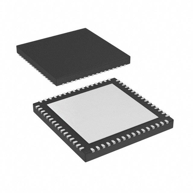


 工商网监
湘ICP备2023018690号
工商网监
湘ICP备2023018690号
