Product
Folder
Order
Now
Support &
Community
Tools &
Software
Technical
Documents
ADS54J60
SBAS706D – APRIL 2015 – REVISED APRIL 2019
ADS54J60 Dual-Channel, 16-Bit, 1.0-GSPS Analog-to-Digital Converter
1 Features
3 Description
•
•
•
The ADS54J60 is a low-power, wide-bandwidth, 16bit,
1.0-GSPS,
dual-channel,
analog-to-digital
converter (ADC). Designed for high signal-to-noise
ratio (SNR), the device delivers a noise floor of
–159 dBFS/Hz for applications aiming for highest
dynamic range over a wide instantaneous bandwidth.
The device supports the JESD204B serial interface
with data rates up to 10 Gbps, supporting two or four
lanes per ADC. The buffered analog input provides
uniform input impedance across a wide frequency
range while minimizing sample-and-hold glitch
energy. Each ADC channel optionally can be
connected to a wideband digital down-converter
(DDC) block. The ADS54J60 provides excellent
spurious-free dynamic range (SFDR) over a large
input frequency range with very low power
consumption.
1
•
•
•
•
•
•
•
•
•
16-bit resolution, dual-channel, 1-GSPS ADC
Noise floor: –159 dBFS/Hz
Spectral performance (fIN = 170 MHz at –1 dBFS):
– SNR: 70 dBFS
– NSD: –157 dBFS/Hz
– SFDR: 86 dBc (including interleaving tones)
– SFDR: 89 dBc (except HD2, HD3, and
interleaving tones)
Spectral performance (fIN = 350 MHz at –1 dBFS):
– SNR: 67.5 dBFS
– NSD: –154.5 dBFS/Hz
– SFDR: 75 dBc
– SFDR: 85 dBc (except HD2, HD3, and
interleaving tones)
Channel isolation: 100 dBc at fIN = 170 MHz
Input full-scale: 1.9 VPP
Input bandwidth (3 dB): 1.2 GHz
On-chip dither
Integrated wideband DDC block
JESD204B interface with subclass 1 support:
– 2 lanes per ADC at 10.0 Gbps
– 4 lanes per ADC at 5.0 Gbps
– Support for multi-chip synchronization
Power dissipation: 1.35 W/Ch at 1 GSPS
Package: 72-pin VQFNP (10 mm × 10 mm)
The JESD204B interface reduces the number of
interface lines, allowing high system integration
density. An internal phase-locked loop (PLL)
multiplies the ADC sampling clock to derive the bit
clock that is used to serialize the 16-bit data from
each channel.
Device Information
PART NUMBER
ADS54J60
FFT for 170-MHz Input Signal
0
SNR = 70 dBFS
SFDR = 86 dBc
Non HD2,HD3 = 89 dBc
-20
Amplitude (dBFS)
Radar and antenna arrays
Broadband wireless
Cable CMTS, DOCSIS 3.1 receivers
Communications test equipment
Microwave receivers
Software-defined radio (SDR)
Digitizers
Medical imaging and diagnostics
BODY SIZE (NOM)
10.00 mm × 10.00 mm
(1) For all available packages, see the orderable addendum at
the end of the data sheet.
2 Applications
•
•
•
•
•
•
•
•
PACKAGE
VQFNP (72)
-40
-60
-80
-100
-120
0
100
200
300
Input Frequency (MHz)
400
500
D000
1
An IMPORTANT NOTICE at the end of this data sheet addresses availability, warranty, changes, use in safety-critical applications,
intellectual property matters and other important disclaimers. PRODUCTION DATA.
�ADS54J60
SBAS706D – APRIL 2015 – REVISED APRIL 2019
www.ti.com
Table of Contents
1
2
3
4
5
6
7
Features ..................................................................
Applications ...........................................................
Description .............................................................
Revision History.....................................................
Device Comparison Table.....................................
Pin Configuration and Functions .........................
Specifications.........................................................
7.1
7.2
7.3
7.4
7.5
7.6
7.7
7.8
7.9
7.10
8
1
1
1
2
5
5
7
Absolute Maximum Ratings ...................................... 7
ESD Ratings.............................................................. 7
Recommended Operating Conditions....................... 7
Thermal Information .................................................. 8
Electrical Characteristics........................................... 8
AC Characteristics .................................................... 9
Digital Characteristics ............................................. 12
Timing Requirements .............................................. 13
Typical Characteristics ............................................ 15
Typical Characteristics: Contour ........................... 24
Detailed Description ............................................ 25
8.1 Overview ................................................................. 25
8.2 Functional Block Diagram ....................................... 25
8.3 Feature Description................................................. 26
8.4 Device Functional Modes........................................ 34
8.5 Register Maps ......................................................... 45
9
Application and Implementation ........................ 74
9.1 Application Information............................................ 74
9.2 Typical Application .................................................. 83
10 Power Supply Recommendations ..................... 85
10.1 Power Sequencing and Initialization ..................... 86
11 Layout................................................................... 87
11.1 Layout Guidelines ................................................. 87
11.2 Layout Example .................................................... 88
12 Device and Documentation Support ................. 89
12.1
12.2
12.3
12.4
12.5
12.6
Documentation Support ........................................
Receiving Notification of Documentation Updates
Community Resources..........................................
Trademarks ...........................................................
Electrostatic Discharge Caution ............................
Glossary ................................................................
89
89
89
89
89
89
13 Mechanical, Packaging, and Orderable
Information ........................................................... 89
4 Revision History
NOTE: Page numbers for previous revisions may differ from page numbers in the current version.
Changes from Revision C (January 2017) to Revision D
Page
•
Changed FFT for 170-MHz Input Signal figure ...................................................................................................................... 1
•
Changed the description of the CLKINM, CLKINP, SYSREFM, SYSREFP, and PDN pins in Pin Functions table .............. 6
•
Changed typical values across parameters in AC Characteristics table................................................................................ 9
•
Changed value of AIN from –1 dBFS to –3 dBFS in 470 MHz test condition across all parameters in AC
Characteristics table ............................................................................................................................................................... 9
•
Added ENOB parameter to AC Characteristics table .......................................................................................................... 11
•
Changed the first footnote in Timing Characteristics table................................................................................................... 13
•
Changed the typical value of FOVR latency from 18 + 4 ns to 18 in Timing Characteristics table ..................................... 13
•
Changed parameter name from tPD to tPDI in Timing Characteristics table .......................................................................... 13
•
Changed FFT for 170-MHz Input Signal figure .................................................................................................................... 15
•
Changed FFT for 470-MHz Input Signal at –3 dBFS figure, title, and conditions ................................................................ 16
•
Changed conditions of FFT for 720-MHz Input Signal at –6 dBFS figure............................................................................ 16
•
Changed Spurious-Free Dynamic Range vs Input Frequency figure................................................................................... 17
•
Changed DDC Block figure .................................................................................................................................................. 27
•
Deleted register address 53 from Register Address for Power-Down Modes table............................................................. 33
•
Added last sentence to Step 4 in Serial Register Readout: Analog Bank section ............................................................... 36
•
Added last sentence to Step 4 in Serial Register Readout: JESD Bank section ................................................................ 37
•
Added SDOUT Timing Diagram figure ................................................................................................................................. 38
•
Deleted unrelated patterns in in JESD204B Test Patterns section...................................................................................... 40
•
Changed Serial Interface Registers figure............................................................................................................................ 45
•
Added register addresses 1h and 2h and their descriptions to GENERAL REGISTERS in Register Map section ............. 46
•
Changed the name of MASTER PAGE (80h) to MASTER PAGE (ANALOG BANK PAGE SEL= 80h in Register Map
table ...................................................................................................................................................................................... 46
•
Changed register 53h and 54h, and their descriptions to MASTER PAGE (ANALOG BANK PAGE SEL = 80h) in
2
Submit Documentation Feedback
Copyright © 2015–2019, Texas Instruments Incorporated
Product Folder Links: ADS54J60
�ADS54J60
www.ti.com
SBAS706D – APRIL 2015 – REVISED APRIL 2019
Revision History (continued)
Register Map section............................................................................................................................................................ 46
•
Changed the name of ADC PAGE (0Fh) to ADC PAGE (ANALOG BANK PAGE SEL= 0Fh) in Register Map table......... 46
•
Changed the name of MAIN DIGITAL PAGE (6800h) to MAIN DIGITAL PAGE (JESD BANK PAGE SEL=6800h) in
Register Map table ............................................................................................................................................................... 46
•
Changed bit 5, register 4E of MAIN DIGITAL PAGE (JESD BANK PAGE SEL = 6800h) from 0 to IMPROVE IL
PERF ................................................................................................................................................................................... 46
•
Changed the name of JESD DIGITAL PAGE (6900h) to JESD DIGITAL PAGE (JESD BANK PAGE SEL=6900h) in
Register Map table ............................................................................................................................................................... 47
•
Changed the name of JESD ANALOG PAGE (6A00h) to JESD ANALOG PAGE (JESD BANK PAGE SEL=6A00h)
in Register Map table............................................................................................................................................................ 47
•
Changed bit 1, register 12 of JESD ANALOG PAGE (6A00h) from 0 to ALWAYS WRITE 1 ............................................. 47
•
Changed bits 5 and 3, register 17 of JESD ANALOG PAGE (JESD BANK PAGE SEL = 6A00h) from 0 to LANE
PDN 1 and from 0 to LANE PDN 0 respectively .................................................................................................................. 47
•
Added OFFSET READ Page and OFFSET LOAD Page registers to Register Map table................................................... 47
•
Added ADS54J60 Access Type Codes table, deleted legends from Register Descriptions section ................................... 49
•
Added register 1h and 2h to Register Descriptions section ................................................................................................ 50
•
Changed description of Registers 3h and 4h (address = 3h and 4h) in General Registers Page ....................................... 51
•
Changed description of bit 0 in Register 4Fh (address = 4Fh), Master Page (080h) .......................................................... 55
•
Changed the description of registers 53h and 54h .............................................................................................................. 56
•
Changed 9.5 dB to 12 dB in description of bits 6-0 in Register 44h (address = 44h), Main Digital Page (6800h).............. 59
•
Changed bit 5 from 0 the IMPROVE IL PERF and changed Register 4Eh Field Descriptions table in Register 4Eh
(address = 4Eh), Main Digital Page (6800h) ........................................................................................................................ 61
•
Changed bit 1 from 0 to ALWAYS WRITE 1 in Register 12h (address = 12h), JESD Analog Page (6A00h) ..................... 68
•
Changed bit 1 from ALWAYS WRITE 1 to 0 in register 15h bit register ............................................................................. 69
•
Added x (where x = 0, 2, or 3) to bits 7-2 in Register 13h-15h Field Descriptions table of Registers 13h-15h
(address = 13h-15h), JESD Analog Page (6A00h) .............................................................................................................. 69
•
Changed bit 6 from W to R/W, bit 5 from 0 to LANE PDN 1 and from W to R/W, and changed bit 3 from 0 to LANE
PDN 0 and from W to R/W in Register 17h bit register table of Register 17h (address = 17h), JESD Analog Page
(6A00h) ................................................................................................................................................................................. 70
•
Changed bits 5-0 of Register 17h Field Descriptions table in Register 17h (address = 17h), JESD Analog Page
(6A00h) ................................................................................................................................................................................. 70
•
Added Offset Read Page Register and Offset Load Page Register sections to Register Descriptions section .................. 72
•
Added DC Offset Correction Block in the ADS54J60 section .............................................................................................. 78
•
Changed ±512 codes to ±1024 codes in DC Offset Correction Block in the ADS54J60 section......................................... 78
•
Added Idle Channel Histogram section ................................................................................................................................ 82
•
Added transformer TC1-1-13M+ to Transformer-Coupled Circuits section.......................................................................... 84
•
Added note to Layout Guidelines section............................................................................................................................. 87
Changes from Revision B (August 2015) to Revision C
Page
•
Changed the SFDR value in the last sub-bullet of the Spectral Performance Features bullet .............................................. 1
•
Changed Device Information table ......................................................................................................................................... 1
•
Added CDM row to ESD Ratings table................................................................................................................................... 7
•
Changed the minimum value for the input clock frequency in the Recommended Operating Conditions table ................... 7
•
Added minimum value to the ADC sampling rate parameter in the Electrical Characteristics table...................................... 8
•
Added 720 -MHz test condition rows to SNR, NSD, SINAD, SFDR, HD2, HD3, Non HD2, HD3, THD, and SFDR_IL
parameters of AC Characteristics table.................................................................................................................................. 9
•
Changed typical specification of SFDR parameter in AC Characteristics table ................................................................... 10
Submit Documentation Feedback
Copyright © 2015–2019, Texas Instruments Incorporated
Product Folder Links: ADS54J60
3
�ADS54J60
SBAS706D – APRIL 2015 – REVISED APRIL 2019
www.ti.com
•
Changed Sample Timing, Aperture jitter parameter typical specification in Timing Characteristics section........................ 13
•
Added the FOVR latency parameter to the Timing Characteristics table............................................................................. 13
•
Added FFT for 720-MHz Input Signal at –6 dBFS figure ..................................................................................................... 16
•
Added Typical Characteristics: Contour section................................................................................................................... 24
•
Changed Overview section .................................................................................................................................................. 25
•
Changed Functional Block Diagram section: changed Control and SPI block and added dashed outline to FOVR traces 25
•
Added Figure 60 and text reference to Analog Inputs section ............................................................................................. 27
•
Changed SYSREF Signal section: changed Table 4 and added last paragraph................................................................. 30
•
Added SYSREF Not Present (Subclass 0, 2) section .......................................................................................................... 31
•
Changed the number of clock cycles in the Fast OVR section ............................................................................................ 32
•
Changed Table 10 and Table 11.......................................................................................................................................... 41
•
Changed Table 12 and Table 13.......................................................................................................................................... 42
•
Deleted Lane Enable with Decimation subsection .............................................................................................................. 42
•
Added the Program Summary of DDC Modes and JESD Link Configuration table............................................................. 43
•
Added Figure 84 to Register Maps section .......................................................................................................................... 45
•
Changed Table 15 ................................................................................................................................................................ 46
•
Deleted register 39h, 3Ah, and 56h ..................................................................................................................................... 46
•
Changed Example Register Writes section .......................................................................................................................... 49
•
Updated register descriptions .............................................................................................................................................. 50
•
Added Table 54 .................................................................................................................................................................... 64
•
Deleted row for bit 1 in Table 64 as bit 1 is included in last table row ................................................................................ 69
•
Changed Table 75 ................................................................................................................................................................ 75
•
Changed internal aperture jitter value in SNR and Clock Jitter section ............................................................................... 78
•
Changed Figure 141............................................................................................................................................................. 78
•
Changed Power Supply Recommendations section ........................................................................................................... 85
•
Added the Power Sequencing and Initialization section....................................................................................................... 86
•
Added Documentation Support and Receiving Notification of Documentation Updates sections........................................ 89
Changes from Revision A (May 2015) to Revision B
•
4
Page
Released to production .......................................................................................................................................................... 1
Submit Documentation Feedback
Copyright © 2015–2019, Texas Instruments Incorporated
Product Folder Links: ADS54J60
�ADS54J60
www.ti.com
SBAS706D – APRIL 2015 – REVISED APRIL 2019
5 Device Comparison Table
PART NUMBER
SPEED GRADE (MSPS)
RESOLUTION (Bits)
CHANNEL
ADS54J20
1000
12
2
ADS54J42
625
14
2
ADS54J40
1000
14
2
ADS54J60
1000
16
2
ADS54J66
500
14
4
ADS54J69
500
16
2
6 Pin Configuration and Functions
DB2P
DB2M
IOVDD
DB1P
DB1M
DGND
DB0P
DB0M
IOVDD
SYNC
DA0M
DA0P
DGND
DA1M
DA1P
IOVDD
DA2M
DA2P
RMP Package
72-Pin VQFNP
Top View
72
71
70
69
68
67
66
65
64
63
62
61
60
59
58
57
56
55
DB3M
1
54
DA3M
DB3P
2
53
DA3P
DGND
3
52
DGND
IOVDD
4
51
IOVDD
SDIN
5
50
PDN
SCLK
6
49
RES
SEN
7
48
RESET
DVDD
8
47
DVDD
AVDD
9
46
AVDD
AVDD3V
10
45
AVDD3V
SDOUT
11
44
AVDD
AVDD
12
43
AVDD
INBP
13
42
INAP
INBM
14
41
INAM
AVDD
15
40
AVDD
AVDD3V
16
39
AVDD3V
AVDD
17
38
AVDD
AGND
18
37
AGND
22
23
24
25
26
27
28
29
30
31
32
33
NC
NC
VCM
AGND
AVDD3V
AVDD
AGND
CLKINP
CLKINM
AGND
AVDD
AVDD3V
AGND
SYSREFP
34
35
36
AGND
21
AVDD
20
SYSREFM
19
NC
GND Pad
(Back Side)
Submit Documentation Feedback
Copyright © 2015–2019, Texas Instruments Incorporated
Product Folder Links: ADS54J60
5
�ADS54J60
SBAS706D – APRIL 2015 – REVISED APRIL 2019
www.ti.com
Pin Functions
PIN
NAME
NO.
I/O
DESCRIPTION
CLOCK, SYSREF
CLKINM
28
I
Negative differential clock input for the ADC. The device has an internal 100-Ω termination
resistor between the CLKINP and CLKINM pins.
CLKINP
27
I
Positive differential clock input for the ADC. The device has an internal 100-Ω termination
resistor between the CLKINP and CLKINM pins.
SYSREFM
34
I
Negative external SYSREF input. Connect this pin to GND if not used.
SYSREFP
33
I
Positive external SYSREF input. Connect this pin to 1.8 V if not used.
PDN
50
I/O
RESET
48
I
Hardware reset; active high. This pin has an internal 20-kΩ pulldown resistor.
SCLK
6
I
Serial interface clock input
SDIN
5
I
Serial interface data input
SDOUT
11
O
Serial interface data output.
Can be configured to fast overrange output for channel B via the SPI.
SEN
7
I
Serial interface enable
O
JESD204B serial data negative outputs for channel A
O
JESD204B serial data positive outputs for channel A
O
JESD204B serial data negative outputs for channel B
O
JESD204B serial data positive outputs for channel B
CONTROL, SERIAL
Power down, active low pin. Can be configured via an SPI register setting.
Can be configured to fast overrange output for channel A via the SPI.
DATA INTERFACE
DA0M
62
DA1M
59
DA2M
56
DA3M
54
DA0P
61
DA1P
58
DA2P
55
DA3P
53
DB0M
65
DB1M
68
DB2M
71
DB3M
1
DB0P
66
DB1P
69
DB2P
72
DB3P
2
SYNC
63
I
Synchronization input for JESD204B port
INAM
41
I
Differential analog negative input for channel A
INAP
42
I
Differential analog positive input for channel A
INBM
14
I
Differential analog negative input for channel B
INBP
13
I
Differential analog positive input for channel B
VCM
22
O
Common-mode voltage, 2.1 V.
Note that analog inputs are internally biased to this pin through 600 Ω (effective), no external
connection from the VCM pin to the INxP or INxM pin is required.
AGND
18, 23, 26, 29, 32, 36, 37
I
Analog ground
AVDD
9, 12, 15, 17, 25, 30, 35, 38,
40, 43, 44, 46
I
Analog 1.9-V power supply
INPUT, COMMON MODE
POWER SUPPLY
AVDD3V
10, 16, 24, 31, 39, 45
I
Analog 3.0-V power supply for the analog buffer
DGND
3, 52, 60, 67
I
Digital ground
DVDD
8, 47
I
Digital 1.9-V power supply
IOVDD
4, 51, 57, 64, 70
I
Digital 1.15-V power supply for the JESD204B transmitter
19-21
—
49
I
NC, RES
NC
RES
6
Unused pins, do not connect
Reserved pin. Connect to DGND.
Submit Documentation Feedback
Copyright © 2015–2019, Texas Instruments Incorporated
Product Folder Links: ADS54J60
�ADS54J60
www.ti.com
SBAS706D – APRIL 2015 – REVISED APRIL 2019
7 Specifications
7.1 Absolute Maximum Ratings
over operating free-air temperature range (unless otherwise noted) (1)
Supply voltage range
MIN
MAX
AVDD3V
–0.3
3.6
AVDD
–0.3
2.1
DVDD
–0.3
2.1
IOVDD
–0.2
1.4
Voltage between AGND and DGND
Voltage applied to input pins
–0.3
0.3
INAP, INBP, INAM, INBM
–0.3
3
CLKINP, CLKINM
–0.3
AVDD + 0.3
SYSREFP, SYSREFM
–0.3
AVDD + 0.3
SCLK, SEN, SDIN, RESET, SYNC, PDN
–0.2
2.1
–65
150
Storage temperature, Tstg
(1)
UNIT
V
V
V
°C
Stresses beyond those listed under Absolute Maximum Ratings may cause permanent damage to the device. These are stress ratings
only, which do not imply functional operation of the device at these or any other conditions beyond those indicated under Recommended
Operating Conditions. Exposure to absolute-maximum-rated conditions for extended periods may affect device reliability.
7.2 ESD Ratings
VALUE
V(ESD)
(1)
(2)
Electrostatic discharge
Human-body model (HBM), per ANSI/ESDA/JEDEC JS-001 (1)
±1000
Charged-device model (CDM), per JEDEC specification JESD22-C101 (2)
±500
UNIT
V
JEDEC document JEP155 states that 500-V HBM allows safe manufacturing with a standard ESD control process.
JEDEC document JEP157 states that 250-V HBM allows safe manufacturing with a standard ESD control process.
7.3 Recommended Operating Conditions
over operating free-air temperature range (unless otherwise noted) (1) (2)
MIN
NOM
MAX
2.85
3.0
3.6
AVDD
1.8
1.9
2.0
DVDD
1.7
1.9
2.0
IOVDD
1.1
1.15
1.2
AVDD3V
Supply voltage range
Analog inputs
1.9
VPP
Input common-mode voltage
2.0
V
(3) (4)
Input clock frequency, device clock frequency
Sine wave, ac-coupled
Input clock amplitude differential
(VCLKP – VCLKM)
LVPECL, ac-coupled
400
250 (5)
Input device clock duty cycle
1.5
0.8
1.6
(1)
(2)
(3)
(4)
(5)
(6)
50%
–40
Operating junction, TJ
MHz
VPP
0.7
45%
Operating free-air, TA
MHz
1000
0.75
LVDS, ac-coupled
Temperature
V
Differential input voltage range
Maximum analog input frequency for 1.9-VPP input amplitude
Clock inputs
UNIT
55%
85
105
(6)
125
ºC
SYSREF must be applied for the device to initialize; see the SYSREF Signal section for details.
After power-up, always use a hardware reset to reset the device for the first time; see Table 75 for details.
Operating 0.5 dB below the maximum-supported amplitude is recommended to accommodate gain mismatch in interleaving ADCs.
At high frequencies, the maximum supported input amplitude reduces; see Figure 37 for details.
See Table 10.
Prolonged use above the nominal junction temperature can increase the device failure-in-time (FIT) rate.
Submit Documentation Feedback
Copyright © 2015–2019, Texas Instruments Incorporated
Product Folder Links: ADS54J60
7
�ADS54J60
SBAS706D – APRIL 2015 – REVISED APRIL 2019
www.ti.com
7.4 Thermal Information
ADS54J60
THERMAL METRIC (1)
RMP (VQFNP)
UNIT
72 PINS
RθJA
Junction-to-ambient thermal resistance
22.3
°C/W
RθJC(top)
Junction-to-case (top) thermal resistance
5.1
°C/W
RθJB
Junction-to-board thermal resistance
2.4
°C/W
ψJT
Junction-to-top characterization parameter
0.1
°C/W
ψJB
Junction-to-board characterization parameter
2.3
°C/W
RθJC(bot)
Junction-to-case (bottom) thermal resistance
0.4
°C/W
(1)
For more information about traditional and new thermal metrics, see the Semiconductor and IC Package Thermal Metrics application
report.
7.5 Electrical Characteristics
typical values are at TA = 25°C, full temperature range is from TMIN = –40°C to TMAX = 85°C, ADC sampling rate = 1.0 GSPS,
50% clock duty cycle, AVDD3V = 3.0 V, AVDD = DVDD = 1.9 V, IOVDD = 1.15 V, –1-dBFS differential input, and 0-dB digital
gain (unless otherwise noted)
PARAMETER
TEST CONDITIONS
MIN
TYP
MAX
UNIT
1000
MSPS
GENERAL
ADC sampling rate
250
Resolution
16
Bits
POWER SUPPLIES
AVDD3V
3.0-V analog supply
2.85
3.0
3.6
V
AVDD
1.9-V analog supply
1.8
1.9
2.0
V
DVDD
1.9-V digital supply
1.7
1.9
2.0
V
IOVDD
1.15-V SERDES supply
1.1
1.15
1.2
V
IAVDD3V
3.0-V analog supply current
VIN = full-scale on both channels
334
360
mA
IAVDD
1.9-V analog supply current
VIN = full-scale on both channels
359
510
mA
IDVDD
1.9-V digital supply current
Eight lanes active (LMFS = 8224)
197
260
mA
IIOVDD
1.15-V SERDES supply current
Eight lanes active (LMFS = 8224)
566
920
mA
Pdis
Total power dissipation
Eight lanes active (LMFS = 8224)
2.71
3.1
W
IDVDD
1.9-V digital supply current
Four lanes active (LMFS = 4244)
211
mA
IIOVDD
1.15-V SERDES supply current
Four lanes active (LMFS = 4244)
618
mA
Pdis
Total power dissipation
Four lanes active (LMFS = 4244)
2.80
W
IDVDD
1.9-V digital supply current
Four lanes active (LMFS = 4222),
2X decimation
197
mA
IIOVDD
1.15-V SERDES supply current
Four lanes active (LMFS = 4222),
2X decimation
593
mA
Pdis
Total power dissipation
Four lanes active (LMFS = 4222),
2X decimation
2.74
W
IDVDD
1.9-V digital supply current
Two lanes active (LMFS = 2221),
4X decimation
176
mA
IIOVDD
1.15-V SERDES supply current
Two lanes active (LMFS = 2221),
4X decimation
562
mA
Pdis (1)
Total power dissipation
Two lanes active (LMFS = 2221),
4X decimation
2.66
W
Global power-down power dissipation
(1)
8
139
315
mW
See the Power-Down Mode section for details.
Submit Documentation Feedback
Copyright © 2015–2019, Texas Instruments Incorporated
Product Folder Links: ADS54J60
�ADS54J60
www.ti.com
SBAS706D – APRIL 2015 – REVISED APRIL 2019
Electrical Characteristics (continued)
typical values are at TA = 25°C, full temperature range is from TMIN = –40°C to TMAX = 85°C, ADC sampling rate = 1.0 GSPS,
50% clock duty cycle, AVDD3V = 3.0 V, AVDD = DVDD = 1.9 V, IOVDD = 1.15 V, –1-dBFS differential input, and 0-dB digital
gain (unless otherwise noted)
PARAMETER
TEST CONDITIONS
MIN
TYP
MAX
UNIT
ANALOG INPUTS (INAP, INAM, INBP, INBM)
Differential input full-scale voltage
1.9
VPP
VIC
Common-mode input voltage
2.0
V
RIN
Differential input resistance
At 170-MHz input frequency
0.6
kΩ
CIN
Differential input capacitance
At 170-MHz input frequency
4.7
pF
Analog input bandwidth (3 dB)
50-Ω source driving ADC inputs
terminated with 50-Ω
1.2
GHz
1.15
V
CLOCK INPUT (CLKINP, CLKINM)
Internal clock biasing
CLKINP and CLKINM are
connected to internal biasing
voltage through 400-Ω
7.6 AC Characteristics
typical values are at TA = 25°C, full temperature range is from TMIN = –40°C to TMAX = 85°C, ADC sampling rate = 1.0 GSPS,
50% clock duty cycle, AVDD3V = 3.0 V, AVDD = DVDD = 1.9 V, IOVDD = 1.15 V, –1-dBFS differential input, and 0-dB digital
gain (unless otherwise noted)
PARAMETER
TEST CONDITIONS
MIN
fIN = 10 MHz, AIN = –1 dBFS
SNR
Signal-to-noise ratio
fIN = 270 MHz, AIN = –1 dBFS
68.7
fIN = 300 MHz, AIN = –1 dBFS
68.1
fIN = 370 MHz, AIN = –1 dBFS
67.1
fIN = 470 MHz, AIN = –3 dBFS
67.6
fIN = 720 MHz, AIN = –6 dBFS
66
fIN = 720 MHz, AIN = –6 dBFS,
gain = 5 dB
64.4
dBFS
157.9
fIN = 100 MHz, AIN = –1 dBFS
Noise spectral density
70
69.2
fIN = 10 MHz, AIN = –1 dBFS
NSD
UNIT
70.6
67.2
fIN = 230 MHz, AIN = –1 dBFS
fIN = 170 MHz, AIN = –1 dBFS
MAX
70.9
fIN = 100 MHz, AIN = –1 dBFS
fIN = 170 MHz, AIN = –1 dBFS
TYP
157.6
154.2
157
fIN = 230 MHz, AIN = –1 dBFS
156.2
fIN = 270 MHz, AIN = –1 dBFS
155.7
fIN = 300 MHz, AIN = –1 dBFS
155.1
fIN = 370 MHz, AIN = –1 dBFS
154.1
fIN = 470 MHz, AIN = –3 dBFS
154.6
fIN = 720 MHz, AIN = –6 dBFS
153
fIN = 720 MHz, AIN = –6 dBFS,
gain = 5 dB
151.4
dBFS/Hz
Submit Documentation Feedback
Copyright © 2015–2019, Texas Instruments Incorporated
Product Folder Links: ADS54J60
9
�ADS54J60
SBAS706D – APRIL 2015 – REVISED APRIL 2019
www.ti.com
AC Characteristics (continued)
typical values are at TA = 25°C, full temperature range is from TMIN = –40°C to TMAX = 85°C, ADC sampling rate = 1.0 GSPS,
50% clock duty cycle, AVDD3V = 3.0 V, AVDD = DVDD = 1.9 V, IOVDD = 1.15 V, –1-dBFS differential input, and 0-dB digital
gain (unless otherwise noted)
PARAMETER
TEST CONDITIONS
Signal-to-noise and distortion ratio
fIN = 100 MHz, AIN = –1 dBFS
70.4
67
69.1
fIN = 270 MHz, AIN = –1 dBFS
68.3
fIN = 300 MHz, AIN = –1 dBFS
67.6
fIN = 370 MHz, AIN = –1 dBFS
66
fIN = 470 MHz, AIN = –3 dBFS
66.8
fIN = 720 MHz, AIN = –6 dBFS
65.2
fIN = 720 MHz, AIN = –6 dBFS,
gain = 5 dB
64.3
Spurious-free dynamic range
(excluding IL spurs)
Second-order harmonic distortion
fIN = 270 MHz, AIN = –1 dBFS
81
fIN = 300 MHz, AIN = –1 dBFS
78
fIN = 370 MHz, AIN = –1 dBFS
73
fIN = 470 MHz, AIN = –3 dBFS
72
fIN = 720 MHz, AIN = –6 dBFS
68
fIN = 720 MHz, AIN = –6 dBFS,
gain = 5 dB
72
fIN = 10 MHz, AIN = –1 dBFS
85
10
Third-order harmonic distortion
95
fIN = 230 MHz, AIN = –1 dBFS
86
fIN = 270 MHz, AIN = –1 dBFS
81
fIN = 300 MHz, AIN = –1 dBFS
81
fIN = 370 MHz, AIN = –1 dBFS
76
fIN = 470 MHz, AIN = –3 dBFS
72
fIN = 720 MHz, AIN = –6 dBFS
68
fIN = 720 MHz, AIN = –6 dBFS,
gain = 5 dB
72
fIN = 10 MHz, AIN = –1 dBFS
87
fIN = 170 MHz, AIN = –1 dBFS
dBc
84
82
89
fIN = 230 MHz, AIN = –1 dBFS
92
fIN = 270 MHz, AIN = –1 dBFS
82
fIN = 300 MHz, AIN = –1 dBFS
78
fIN = 370 MHz, AIN = –1 dBFS
73
fIN = 470 MHz, AIN = –3 dBFS
70
fIN = 720 MHz, AIN = –6 dBFS
75
fIN = 720 MHz, AIN = –6 dBFS,
gain = 5 dB
84
Submit Documentation Feedback
dBc
92
79
fIN = 100 MHz, AIN = –1 dBFS
HD3
88
86
fIN = 100 MHz, AIN = –1 dBFS
HD2
dBFS
84
78
fIN = 230 MHz, AIN = –1 dBFS
fIN = 170 MHz, AIN = –1 dBFS
UNIT
85
fIN = 100 MHz, AIN = –1 dBFS
fIN = 170 MHz, AIN = –1 dBFS
MAX
69.8
fIN = 230 MHz, AIN = –1 dBFS
fIN = 10 MHz, AIN = –1 dBFS
SFDR
TYP
70.7
fIN = 170 MHz, AIN = –1 dBFS
SINAD
MIN
fIN = 10 MHz, AIN = –1 dBFS
dBc
Copyright © 2015–2019, Texas Instruments Incorporated
Product Folder Links: ADS54J60
�ADS54J60
www.ti.com
SBAS706D – APRIL 2015 – REVISED APRIL 2019
AC Characteristics (continued)
typical values are at TA = 25°C, full temperature range is from TMIN = –40°C to TMAX = 85°C, ADC sampling rate = 1.0 GSPS,
50% clock duty cycle, AVDD3V = 3.0 V, AVDD = DVDD = 1.9 V, IOVDD = 1.15 V, –1-dBFS differential input, and 0-dB digital
gain (unless otherwise noted)
PARAMETER
TEST CONDITIONS
Spurious-free dynamic range
(excluding HD2, HD3, and IL spur)
fIN = 100 MHz, AIN = –1 dBFS
97
79
95
fIN = 270 MHz, AIN = –1 dBFS
95
fIN = 300 MHz, AIN = –1 dBFS
91
fIN = 370 MHz, AIN = –1 dBFS
85
fIN = 470 MHz, AIN = –3 dBFS
90
fIN = 720 MHz, AIN = –6 dBFS
90
fIN = 720 MHz, AIN = –6 dBFS,
gain = 5 dB
96
fIN = 10 MHz, AIN = –1 dBFS
83
fIN = 170 MHz, AIN = –1 dBFS
ENOB
Total harmonic distortion
Effective number of bits
fIN = 270 MHz, AIN = –1 dBFS
78
fIN = 300 MHz, AIN = –1 dBFS
76
fIN = 370 MHz, AIN = –1 dBFS
71
fIN = 470 MHz, AIN = –3 dBFS
71
fIN = 720 MHz, AIN = –6 dBFS
67
fIN = 720 MHz, AIN = –6 dBFS,
gain = 5 dB
71
fIN = 10 MHz, AIN = –1 dBFS
11.5
fIN = 100 MHz, AIN = –1 dBFS
11.4
fIN = 170 MHz, AIN = –1 dBFS
11.3
fIN = 230 MHz, AIN = –1 dBFS
11.2
fIN = 270 MHz, AIN = –1 dBFS
11.0
fIN = 300 MHz, AIN = –1 dBFS
10.9
fIN = 370 MHz, AIN = –1 dBFS
10.7
fIN = 470 MHz, AIN = –3 dBFS
10.8
fIN = 720 MHz, AIN = –6 dBFS
10.5
fIN = 720 MHz, AIN = –6 dBFS,
gain = 5 dB
10.4
87
85
fIN = 270 MHz, AIN = –1 dBFS
84
fIN = 300 MHz, AIN = –1 dBFS
82
fIN = 370 MHz, AIN = –1 dBFS
82
fIN = 470 MHz, AIN = –3 dBFS
79
fIN = 720 MHz, AIN = –6 dBFS
79
fIN = 720 MHz, AIN = –6 dBFS,
gain = 5 dB
75
Submit Documentation Feedback
Product Folder Links: ADS54J60
Bits
90
69
fIN = 230 MHz, AIN = –1 dBFS
Copyright © 2015–2019, Texas Instruments Incorporated
dBc
88
fIN = 100 MHz, AIN = –1 dBFS
Interleaving spur
dBFS
87
84
fIN = 10 MHz, AIN = –1 dBFS
SFDR_IL
UNIT
83
74
fIN = 230 MHz, AIN = –1 dBFS
fIN = 170 MHz, AIN = –1 dBFS
MAX
93
fIN = 230 MHz, AIN = –1 dBFS
fIN = 100 MHz, AIN = –1 dBFS
THD
TYP
94
fIN = 170 MHz, AIN = –1 dBFS
Non HD2,
HD3
MIN
fIN = 10 MHz, AIN = –1 dBFS
dBc
11
�ADS54J60
SBAS706D – APRIL 2015 – REVISED APRIL 2019
www.ti.com
AC Characteristics (continued)
typical values are at TA = 25°C, full temperature range is from TMIN = –40°C to TMAX = 85°C, ADC sampling rate = 1.0 GSPS,
50% clock duty cycle, AVDD3V = 3.0 V, AVDD = DVDD = 1.9 V, IOVDD = 1.15 V, –1-dBFS differential input, and 0-dB digital
gain (unless otherwise noted)
PARAMETER
TEST CONDITIONS
Two-tone, third-order
intermodulation distortion
IMD3
Crosstalk isolation between channel
A and B
MIN
TYP
fIN1 = 185 MHz, fIN2 = 190 MHz,
AIN = –7 dBFS
–88
fIN1 = 365 MHz, fIN2 = 370 MHz,
AIN = –7 dBFS
–79
fIN1 = 465 MHz, fIN2 = 470 MHz,
AIN = –7 dBFS
–75
Full-scale, 170-MHz signal on
aggressor; idle channel is victim
100
MAX
UNIT
dBFS
dB
7.7 Digital Characteristics
typical values are at TA = 25°C, full temperature range is from TMIN = –40°C to TMAX = 85°C, ADC sampling rate = 1.0 GSPS,
50% clock duty cycle, AVDD3V = 3.0 V, AVDD = DVDD = 1.9 V, IOVDD = 1.15 V, –1-dBFS differential input, and 0-dB digital
gain (unless otherwise noted)
PARAMETER
TEST CONDITIONS
MIN
0.8
TYP
MAX
UNITS
DIGITAL INPUTS (RESET, SCLK, SEN, SDIN, SYNC, PDN) (1)
VIH
High-level input voltage
All digital inputs support 1.2-V and 1.8-V logic levels
VIL
Low-level input voltage
All digital inputs support 1.2-V and 1.8-V logic levels
IIH
High-level input current
IIL
Low-level input current
V
0.4
SEN
0
RESET, SCLK, SDIN, PDN, SYNC
50
SEN
50
RESET, SCLK, SDIN, PDN, SYNC
V
µA
µA
0
DIGITAL INPUTS (SYSREFP, SYSREFM)
VD
Differential input voltage
V(CM_DIG)
Common-mode voltage for SYSREF
0.35
0.45
1.4
V
1.3
V
DVDD
V
DIGITAL OUTPUTS (SDOUT, PDN (2))
VOH
High-level output voltage
VOL
Low-level output voltage
DVDD –
0.1
0.1
DIGITAL OUTPUTS (JESD204B Interface: DxP, DxM)
VOD
Output differential voltage
VOC
Output common-mode voltage
Transmitter short-circuit current
zos
(1)
(2)
(3)
12
With default swing setting
Transmitter pins shorted to any voltage between
–0.25 V and 1.45 V
Single-ended output impedance
Output capacitance
V
(3)
Output capacitance inside the device,
from either output to ground
700
mVPP
450
mV
–100
100
mA
50
Ω
2
pF
The RESET, SCLK, SDIN, and PDN pins have a 20-kΩ (typical) internal pulldown resistor to ground, and the SEN pin has a 20-kΩ
(typical) pullup resistor to IOVDD.
When functioning as an OVR pin for channel B.
100-Ω differential termination.
Submit Documentation Feedback
Copyright © 2015–2019, Texas Instruments Incorporated
Product Folder Links: ADS54J60
�ADS54J60
www.ti.com
SBAS706D – APRIL 2015 – REVISED APRIL 2019
7.8 Timing Requirements
typical values are at TA = 25°C, full temperature range is from TMIN = –40°C to TMAX = 85°C, ADC sampling rate = 1.0 GSPS,
50% clock duty cycle, AVDD3V = 3.0 V, AVDD = DVDD = 1.9 V, IOVDD = 1.15 V, and –1-dBFS differential input (unless
otherwise noted)
MIN
TYP
MAX
UNITS
SAMPLE TIMING
Aperture delay
0.75
Aperture delay matching between two channels on the same device
1.6
ns
±70
Aperture delay matching between two devices at the same temperature and supply voltage
ps
±270
ps
120
fS rms
150
µs
134
Input
clock
cycles
OVR latency: ADC sample to OVR bit
62
Input
clock
cycles
FOVR latency: ADC sample to FOVR signal on pin
18
Input
clock
cycles
4
ns
Aperture jitter
WAKE-UP TIMING
Wake-up time to valid data after coming out of global power-down
LATENCY
(1)
Data latency: ADC sample to digital output
tPDI
Propagation delay: logic gates and output buffers delay (does not change with fS)
SYSREF TIMING
tSU_SYSREF
Setup time for SYSREF, referenced to the input clock falling edge
300
tH_SYSREF
Hold time for SYSREF, referenced to the input clock falling edge
100
900
ps
ps
JESD OUTPUT INTERFACE TIMING CHARACTERISTICS
Unit interval
100
400
ps
Serial output data rate
2.5
10
Gbps
Total jitter for BER of 1E-15 and lane rate = 10 Gbps
26
Random jitter for BER of 1E-15 and lane rate = 10 Gbps
tR, tF
(1)
0.75
ps
ps rms
Deterministic jitter for BER of 1E-15 and lane rate = 10 Gbps
12
ps, pk-pk
Data rise time, data fall time: rise and fall times are measured from 20% to 80%,
differential output waveform, 2.5 Gbps ≤ bit rate ≤ 10 Gbps
35
ps
Overall latency = latency + tPDI.
Sample N
ts_min
ts_max
CLKIN
1.0 GSPS
SYSREF
Figure 1. SYSREF Timing
Submit Documentation Feedback
Copyright © 2015–2019, Texas Instruments Incorporated
Product Folder Links: ADS54J60
13
�ADS54J60
SBAS706D – APRIL 2015 – REVISED APRIL 2019
N+1
www.ti.com
N+2
N
N+3
Sample
tPD
Data Latency: 134 Clock Cycles
CLKINM
CLKINP
DA0P, DA0M,
DB0P, DB0M
D
20
Sample N-1
DA1P, DA1M,
DB1P, DB1M
Sample N-1
D
11
D
20
Sample N
D
10
D
11
D
20
Sample N+1
D
1
D
10
Sample N
Sample N+2
D
1
Sample N+1
D
10
Sample N+2
Figure 2. Sample Timing Requirements Diagram
14
Submit Documentation Feedback
Copyright © 2015–2019, Texas Instruments Incorporated
Product Folder Links: ADS54J60
�ADS54J60
www.ti.com
SBAS706D – APRIL 2015 – REVISED APRIL 2019
7.9 Typical Characteristics
0
0
-20
-20
Amplitude (dBFS)
Amplitude (dBFS)
typical values are at TA = 25°C, full temperature range is from TMIN = –40°C to TMAX = 85°C, ADC sampling rate = 1.0 GSPS,
50% clock duty cycle, AVDD3V = 3.0 V, AVDD = DVDD = 1.9 V, IOVDD = 1.15 V, and –1-dBFS differential input (unless
otherwise noted)
-40
-60
-80
-40
-60
-80
-100
-100
-120
-120
0
100
200
300
Input Frequency (MHz)
400
0
500
SNR = 71 dBFS; SFDR = 86 dBc;
IL spur = 94 dBc; non HD2, HD3 spur = 89 dBc
400
500
D002
Figure 4. FFT for 140-MHz Input Signal
0
0
-20
-20
Amplitude (dBFS)
Amplitude (dBFS)
200
300
Input Frequency (MHz)
SNR = 70.3 dBFS; SFDR = 90 dBc;
IL spur = 95 dBc; non HD2, HD3 spur = 94 dBc
Figure 3. FFT for 10-MHz Input Signal
-40
-60
-80
-100
-40
-60
-80
-100
-120
-120
0
100
200
300
Input Frequency (MHz)
400
500
0
100
D003
SNR = 69.8 dBFS; SFDR = 88 dBc;
IL spur = 86 dBc; non HD2, HD3 spur = 89 dBc
200
300
Input Frequency (MHz)
400
500
D004
SNR = 68.9 dBFS; SFDR = 85 dBc;
IL spur = 85 dBc; non HD2, HD3 spur = 86 dBc
Figure 5. FFT for 170-MHz Input Signal
Figure 6. FFT for 230-MHz Input Signal
0
0
-20
-20
Amplitude (dBFS)
Amplitude (dBFS)
100
D001
-40
-60
-80
-100
-40
-60
-80
-100
-120
-120
0
100
200
300
Input Frequency (MHz)
400
500
0
D005
100
200
300
Input Frequency (MHz)
400
SNR = 68 dBFS; SFDR = 77 dBc;
IL spur = 84 dBc; non HD2, HD3 spur = 85 dBc
SNR = 66.7 dBFS; SFDR = 71 dBc;
IL spur = 87 dBc; non HD2, HD3 spur = 78 dBc
Figure 7. FFT for 300-MHz Input Signal
Figure 8. FFT for 370-MHz Input Signal
500
D006
Submit Documentation Feedback
Copyright © 2015–2019, Texas Instruments Incorporated
Product Folder Links: ADS54J60
15
�ADS54J60
SBAS706D – APRIL 2015 – REVISED APRIL 2019
www.ti.com
Typical Characteristics (continued)
0
0
-20
-20
Amplitude (dBFS)
Amplitude (dBFS)
typical values are at TA = 25°C, full temperature range is from TMIN = –40°C to TMAX = 85°C, ADC sampling rate = 1.0 GSPS,
50% clock duty cycle, AVDD3V = 3.0 V, AVDD = DVDD = 1.9 V, IOVDD = 1.15 V, and –1-dBFS differential input (unless
otherwise noted)
-40
-60
-80
0
100
200
300
Input Frequency (MHz)
400
0
500
100
D007
200
300
Input Frequency (MHz)
400
500
D058
SNR = 66.3 dBFS, SINAD = 65.3 dBFS, THD = 70 dBc,
IL spur = 84 dBc, SFDR = 73 dBc, non HD2, HD3 spur = 90 dBFS
SNR = 67.9 dBFS; SFDR = 74 dBc;
IL spur = 82 dBc; non HD2, HD3 spur = 89 dBc
Figure 10. FFT for 720-MHz Input Signal at –6 dBFS
Figure 9. FFT for 470-MHz Input Signal at –3 dBFS
0
0
-20
-20
Amplitude (dBFS)
Amplitude (dBFS)
-80
-120
-120
-40
-60
-80
-100
-40
-60
-80
-100
-120
-120
0
100
200
300
Input Frequency (MHz)
400
500
0
100
D008
fIN1 = 185 MHz, fIN2 = 190 MHz, each tone at –7 dBFS,
IMD3 = 88 dBFS
-20
-20
Amplitude (dBFS)
0
-60
-80
-100
400
500
D009
Figure 12. FFT for Two-Tone Input Signal (–36 dBFS)
0
-40
200
300
Input Frequency (MHz)
fIN1 = 185 MHz, fIN2 = 190 MHz, each tone at –36 dBFS,
IMD3 = 106 dBFS
Figure 11. FFT for Two-Tone Input Signal (–7 dBFS)
Amplitude (dBFS)
-60
-100
-100
-40
-60
-80
-100
-120
-120
0
100
200
300
Input Frequency (MHz)
400
500
0
D010
fIN1 = 365 MHz, fIN2 = 370 MHz, each tone at –7 dBFS,
IMD3 = 80 dBFS
Figure 13. FFT for Two-Tone Input Signal (–7 dBFS)
16
-40
100
200
300
Input Frequency (MHz)
400
500
D011
fIN1 = 365 MHz, fIN2 = 370 MHz, each tone at –36 dBFS,
IMD3 = 105 dBFS
Figure 14. FFT for Two-Tone Input Signal (–36 dBFS)
Submit Documentation Feedback
Copyright © 2015–2019, Texas Instruments Incorporated
Product Folder Links: ADS54J60
�ADS54J60
www.ti.com
SBAS706D – APRIL 2015 – REVISED APRIL 2019
Typical Characteristics (continued)
0
0
-20
-20
Amplitude (dBFS)
Amplitude (dBFS)
typical values are at TA = 25°C, full temperature range is from TMIN = –40°C to TMAX = 85°C, ADC sampling rate = 1.0 GSPS,
50% clock duty cycle, AVDD3V = 3.0 V, AVDD = DVDD = 1.9 V, IOVDD = 1.15 V, and –1-dBFS differential input (unless
otherwise noted)
-40
-60
-80
-100
-60
-80
-100
-120
-120
0
100
200
300
Input Frequency (MHz)
400
500
0
100
D012
fIN1 = 465 MHz, fIN2 = 470 MHz, each tone at –7 dBFS,
IMD3 = 75 dBFS
400
500
D013
Figure 15. FFT for Two-Tone Input Signal (–7 dBFS)
Figure 16. FFT for Two-Tone Input Signal (–36 dBFS)
-82
-76
-86
-80
-84
IMD (dBFS)
-94
-98
-102
-110
-35
-88
-92
-96
-100
-106
-104
-31
-27
-23
-19
-15
Each Tone Amplitude (dBFS)
-11
-108
-35
-7
-27
-23
-19
-15
Each Tone Amplitude (dBFS)
-11
-7
D015
fIN1 = 365 MHz, fIN2 = 370 MHz
Figure 17. Intermodulation Distortion vs
Input Tone Amplitude
Figure 18. Intermodulation Distortion vs
Input Tone Amplitude
-70
95
-74
90
-78
AIN = -6 dBFS
AIN = -3 dBFS
AIN = -1 dBFS
85
SFDR (dBc)
-82
-86
-90
-94
80
75
70
65
-98
60
-102
-106
-35
-31
D014
fIN1 = 185 MHz, fIN2 = 190 MHz
IMD (dBFS)
200
300
Input Frequency (MHz)
fIN1 = 465 MHz, fIN2 = 470 MHz, each tone at –36 dBFS,
IMD3 = 106 dBFS
-90
IMD (dBFS)
-40
55
-31
-27
-23
-19
-15
Each Tone Amplitude (dBFS)
-11
-7
0
100
D016
200
300
400
500
Input Frequency (MHz)
600
700
D043
fIN1 = 465 MHz, fIN2 = 470 MHz
Figure 19. Intermodulation Distortion vs
Input Tone Amplitude
Figure 20. Spurious-Free Dynamic Range vs
Input Frequency
Submit Documentation Feedback
Copyright © 2015–2019, Texas Instruments Incorporated
Product Folder Links: ADS54J60
17
�ADS54J60
SBAS706D – APRIL 2015 – REVISED APRIL 2019
www.ti.com
Typical Characteristics (continued)
typical values are at TA = 25°C, full temperature range is from TMIN = –40°C to TMAX = 85°C, ADC sampling rate = 1.0 GSPS,
50% clock duty cycle, AVDD3V = 3.0 V, AVDD = DVDD = 1.9 V, IOVDD = 1.15 V, and –1-dBFS differential input (unless
otherwise noted)
72
95
SNR (dBFS)
Interleaving Spur (dBc)
91
87
83
70
69
68
79
67
66
75
0
40
0
80 120 160 200 240 280 320 360 400 440 480
Input Frequency (MHz)
D018
200
300
400
500
Input Frequency (MHz)
600
700
D042
96
AVDD = 1.8 V
AVDD = 1.85 V
AVDD = 1.9 V
71.5
AVDD = 1.95 V
AVDD = 2 V
92
90
SFDR (dBc)
71
70
69.5
86
84
68.5
82
10
35
Temperature (°C)
60
80
-40
85
AVDD = 1.95 V
AVDD = 2 V
88
69
-15
AVDD = 1.8 V
AVDD = 1.85 V
AVDD = 1.9 V
94
70.5
68
-40
100
Figure 22. Signal-to-Noise Ratio vs Input Frequency
Figure 21. IL Spur vs Input Frequency
72
SNR (dBFS)
AIN = -6 dBFS
AIN = -3 dBFS
AIN = -1 dBFS
71
-15
D020
fIN = 170 MHz
10
35
Temperature (°C)
60
85
D021
fIN = 170 MHz
Figure 23. Signal-to-Noise Ratio vs
AVDD Supply and Temperature
Figure 24. Spurious-Free Dynamic Range vs
AVDD Supply and Temperature
78
72
AVDD = 1.8 V
AVDD = 1.85 V
AVDD = 1.9 V
71
AVDD = 1.95 V
AVDD = 2 V
AVDD = 1.8 V
AVDD = 1.85 V
AVDD = 1.9 V
77
AVDD = 1.95 V
AVDD = 2 V
69
SFDR (dBc)
SNR (dBFS)
70
68
67
76
75
74
66
73
65
64
-40
-15
10
35
Temperature (°C)
60
85
72
-40
-15
D022
fIN = 350 MHz
60
85
D023
fIN = 350 MHz
Figure 25. Signal-to-Noise Ratio vs
AVDD Supply and Temperature
18
10
35
Temperature (°C)
Figure 26. Spurious-Free Dynamic Range vs
AVDD Supply and Temperature
Submit Documentation Feedback
Copyright © 2015–2019, Texas Instruments Incorporated
Product Folder Links: ADS54J60
�ADS54J60
www.ti.com
SBAS706D – APRIL 2015 – REVISED APRIL 2019
Typical Characteristics (continued)
typical values are at TA = 25°C, full temperature range is from TMIN = –40°C to TMAX = 85°C, ADC sampling rate = 1.0 GSPS,
50% clock duty cycle, AVDD3V = 3.0 V, AVDD = DVDD = 1.9 V, IOVDD = 1.15 V, and –1-dBFS differential input (unless
otherwise noted)
72
94
DVDD = 1.75 V
DVDD = 1.8 V
DVDD = 1.85 V
70.4
69.6
68.8
68
-40
DVDD = 1.75 V
DVDD = 1.8 V
DVDD = 1.85 V
92
SFDR (dBc)
SNR (dBFS)
71.2
DVDD = 1.9 V
DVDD = 1.95 V
DVDD = 2 V
90
88
86
-15
10
35
Temperature (°C)
60
84
-40
85
-15
D024
fIN = 170 MHz
10
35
Temperature (°C)
60
85
D025
fIN = 170 MHz
Figure 27. Signal-to-Noise Ratio vs
DVDD Supply and Temperature
Figure 28. Spurious-Free Dynamic Range vs
DVDD Supply and Temperature
72
82
DVDD = 1.75 V
DVDD = 1.8 V
DVDD = 1.85 V
71
DVDD = 1.9 V
DVDD = 1.95 V
DVDD = 2 V
DVDD = 1.75 V
DVDD = 1.8 V
DVDD = 1.85 V
80
70
SFDR (dBc)
SNR (dBFS)
DVDD = 1.9 V
DVDD = 1.95 V
DVDD = 2 V
69
DVDD = 1.9 V
DVDD = 1.95 V
DVDD = 2 V
78
76
68
74
67
66
-40
-15
10
35
Temperature (°C)
60
72
-40
85
-15
D026
fIN = 350 MHz
85
D027
Figure 30. Spurious-Free Dynamic Range vs
DVDD Supply and Temperature
72
97
AVDD3V = 2.85 V
AVDD3V = 3 V
AVDD3V = 3.1 V
AVDD3V = 3.2 V
71.5
AVDD3V = 3.3 V
AVDD3V = 3.4 V
AVDD3V = 3.5 V
AVDD3V = 3.6 V
AVDD3V = 2.85 V
AVDD3V = 3 V
AVDD3V = 3.1 V
AVDD3V = 3.2 V
95
93
71
SFDR (dBc)
SNR (dBFS)
60
fIN = 350 MHz
Figure 29. Signal-to-Noise Ratio vs
DVDD Supply and Temperature
70.5
70
AVDD3V = 3.3 V
AVDD3V = 3.4 V
AVDD3V = 3.5 V
AVDD3V = 3.6 V
91
89
87
69.5
69
-40
10
35
Temperature (°C)
85
-15
10
35
Temperature (°C)
60
85
83
-40
-15
D028
fIN = 170 MHz
10
35
Temperature (°C)
60
85
D029
fIN = 170 MHz
Figure 31. Signal-to-Noise Ratio vs
AVDD3V Supply and Temperature
Figure 32. Spurious-Free Dynamic Range vs
AVDD3V Supply and Temperature
Submit Documentation Feedback
Copyright © 2015–2019, Texas Instruments Incorporated
Product Folder Links: ADS54J60
19
�ADS54J60
SBAS706D – APRIL 2015 – REVISED APRIL 2019
www.ti.com
Typical Characteristics (continued)
typical values are at TA = 25°C, full temperature range is from TMIN = –40°C to TMAX = 85°C, ADC sampling rate = 1.0 GSPS,
50% clock duty cycle, AVDD3V = 3.0 V, AVDD = DVDD = 1.9 V, IOVDD = 1.15 V, and –1-dBFS differential input (unless
otherwise noted)
72
82
AVDD3V = 2.85 V
AVDD3V = 3 V
AVDD3V = 3.1 V
AVDD3V = 3.2 V
71
AVDD3V = 2.85 V
AVDD3V = 3 V
AVDD3V = 3.1 V
AVDD3V = 3.2 V
80
SFDR (dBc)
SNR (dBFS)
70
AVDD3V = 3.3 V
AVDD3V = 3.4 V
AVDD3V = 3.5 V
AVDD3V = 3.6 V
69
68
AVDD3V = 3.3 V
AVDD3V = 3.4 V
AVDD3V = 3.5 V
AVDD3V = 3.6 V
78
76
67
74
66
65
-40
-15
10
35
Temperature (°C)
60
72
-40
85
-15
fIN = 350 MHz
60
85
D031
fIN = 350 MHz
Figure 33. Signal-to-Noise Ratio vs
AVDD3V Supply and Temperature
Figure 34. Spurious-Free Dynamic Range vs
AVDD3V Supply and Temperature
110
85
Gain = 0 dB
Gain = 2 dB
Gain = 4 dB
80
Gain = 6 dB
Gain = 8 dB
Gain = 10 dB
Gain = 0 dB
Gain = 2 dB
Gain = 4 dB
Gain = 12 dB
105
100
75
SFDR (dBc)
SNRFS (dB)
10
35
Temperature (°C)
D030
70
Gain = 6 dB
Gain = 8 dB
Gain = 10 dB
Gain = 12 dB
95
90
85
80
65
75
60
70
65
55
80
160
240
320
Input Frequency (MHz)
400
0
480
Figure 35. Signal-to-Noise Ratio vs
Gain and Input Frequency
160
240
320
Input Frequency (MHz)
400
480
D054
Figure 36. Spurious-Free Dynamic Range vs
Gain and Input Frequency
75
2
0
-2
SNR (dBFS)
Fundamental Amplitude (dBFS)
80
D053
-4
73
200
SNR (dBFS)
SFDR (dBc)
SFDR (dBFS) 160
71
120
69
80
67
40
-6
-8
-10
0
100
200
300 400 500 600 700
Input Frequency (MHz)
800
900 1000
65
-70
SFDR (dBc,dBFS)
0
0
-60
D046
-50
-40
-30
Amplitude (dBFS)
-20
-10
0
D032
fIN = 170 MHz
Figure 37. Maximum Supported Amplitude vs Frequency
20
Figure 38. Performance vs Input Amplitude
Submit Documentation Feedback
Copyright © 2015–2019, Texas Instruments Incorporated
Product Folder Links: ADS54J60
�ADS54J60
www.ti.com
SBAS706D – APRIL 2015 – REVISED APRIL 2019
Typical Characteristics (continued)
typical values are at TA = 25°C, full temperature range is from TMIN = –40°C to TMAX = 85°C, ADC sampling rate = 1.0 GSPS,
50% clock duty cycle, AVDD3V = 3.0 V, AVDD = DVDD = 1.9 V, IOVDD = 1.15 V, and –1-dBFS differential input (unless
otherwise noted)
120
70.5
90
69
60
67.5
30
-50
-40
-30
Amplitude (dBFS)
-20
-10
100
72
90
70
80
68
70
66
0.2
0
-60
74
0
D033
fIN = 350 MHz
Figure 39. Performance vs Input Amplitude
Figure 40. Performance vs Sampling Clock Amplitude
125
73
100
72
100
69
75
66
50
63
25
0
2.2
0.6
1
1.4
1.8
Differential Clock Amplitude (Vpp)
SNR (dBFS)
SNR
SFDR
SFDR (dBc)
SNR
SFDR
SNR (dBFS)
D034
fIN = 170 MHz
75
60
0.2
60
2.2
0.6
1
1.4
1.8
Differential Clock Amplitude (Vpp)
72
95
71
90
70
85
69
80
68
30
35
40
D035
fIN = 350 MHz
45
50
55
60
Input Clock Duty Cycle (%)
65
SFDR (dBc)
66
-70
110
SNR
SFDR
SFDR (dBc)
72
76
SNR (dBFS)
73.5
180
SNR (dBFS)
SFDR (dBc)
SFDR (dBFS) 150
SFDR (dBc,dBFS)
SNR (dBFS)
75
75
70
D036
fIN = 170 MHz
Figure 41. Performance vs Sampling Clock Amplitude
Figure 42. Performance vs Clock Duty Cycle
72
88
-10
71
SNR
SFDR 84
-15
70
80
69
76
68
72
67
68
66
64
PSRR with 50-mVPP Signal on AVDD
PSRR with 50-mVPP Signal on AVDD3V
PSRR (dB)
-25
SFDR (dBc)
SNR (dBFS)
-20
-30
-35
-40
-45
-50
65
30
35
40
45
50
55
60
Input Clock Duty Cycle (%)
65
60
70
-55
-60
0
50
D037
fIN = 350 MHz
100
150
200
250
Frequency of Signal on Supply (MHz)
300
D038
fIN = 170 MHz
Figure 43. Performance vs Clock Duty Cycle
Figure 44. Power-Supply Rejection Ratio vs
Test Signal Frequency
Submit Documentation Feedback
Copyright © 2015–2019, Texas Instruments Incorporated
Product Folder Links: ADS54J60
21
�ADS54J60
SBAS706D – APRIL 2015 – REVISED APRIL 2019
www.ti.com
Typical Characteristics (continued)
0
-20
-20
-25
-40
-30
CMRR (dB)
Amplitude (dBFS)
typical values are at TA = 25°C, full temperature range is from TMIN = –40°C to TMAX = 85°C, ADC sampling rate = 1.0 GSPS,
50% clock duty cycle, AVDD3V = 3.0 V, AVDD = DVDD = 1.9 V, IOVDD = 1.15 V, and –1-dBFS differential input (unless
otherwise noted)
-60
-80
-35
-40
-45
-100
-50
-120
0
100
200
300
Input Frequency (MHz)
400
500
-55
D039
0
fIN = 170 MHz , AIN = –1 dBFS, SINAD = 67 dBFS,
SFDR = 79 dBc, fPSRR = 5 MHz, APSRR = 25 mVPP,
amplitude of fIN – fPSRR = –74 dBFS,
amplitude of fIN + fPSRR = –76 dBFS
300
D040
fIN = 170 MHz
Figure 46. Common-Mode Rejection Ratio vs
Test Signal Frequency
Figure 45. Power-Supply Rejection Ratio FFT for
Test Signals on the AVDD Supply
0
4
-20
3.5
Power Consumption (W)
Amplitude (dBFS)
50
100
150
200
250
Frequency of Input Common-Mode Signal (MHz)
-40
-60
-80
-100
3
2.5
2
1.5
-120
0
100
200
300
Input Frequency (MHz)
400
500
1
500
D041
fIN = 170 MHz , AIN = –1 dBFS, fCMRR = 5 MHz, ACMRR = 50 mVPP,
SINAD = 69.1 dBFS, SFDR = 86 dBc,
amplitude of fIN ± fCMRR= –80 dBFS
550
700
I AVDD3 (mA)
Total Power (W)
2.78
0
2.76
-20
2.74
500
2.72
400
2.7
300
2.68
200
2.66
-100
2.64
85
-120
100
-40
-15
10
35
Temperature (°C)
60
Amplitude (dBFS)
600
Total Power (W)
IAVDD,IDVDD,IAVDD3,IIOVDD (mA)
I DVDD (mA)
I AVDD (mA)
I IOVDD (mA)
650 700 750 800 850
Sampling Speed (MSPS)
900
950 1000
D042
Figure 48. Power vs Sampling Speed
Figure 47. Common-Mode Rejection Ratio FFT
800
600
-40
-60
-80
0
D045
25
50
75
Input Frequency (MHz)
100
125
D047
SNR = 76.4 dBFS, SFDR = 99 dBc
Figure 49. Power vs Temperature
22
Submit Documentation Feedback
Figure 50. FFT for 60-MHz Input Signal in
Decimate-by-4 Mode
Copyright © 2015–2019, Texas Instruments Incorporated
Product Folder Links: ADS54J60
�ADS54J60
www.ti.com
SBAS706D – APRIL 2015 – REVISED APRIL 2019
Typical Characteristics (continued)
0
0
-20
-20
Amplitude (dBFS)
Amplitude (dBFS)
typical values are at TA = 25°C, full temperature range is from TMIN = –40°C to TMAX = 85°C, ADC sampling rate = 1.0 GSPS,
50% clock duty cycle, AVDD3V = 3.0 V, AVDD = DVDD = 1.9 V, IOVDD = 1.15 V, and –1-dBFS differential input (unless
otherwise noted)
-40
-60
-80
-100
-40
-60
-80
-100
-120
-120
0
25
50
75
Input Frequency (MHz)
100
125
0
25
SNR = 75.2 dBFS, SFDR = 90 dBc
100
125
D049
SNR = 72.8 dBFS, SFDR = 91 dBc
Figure 51. FFT for 170-MHz Input Signal in
Decimate-by-4 Mode
Figure 52. FFT for 300-MHz Input Signal in
Decimate-by-4 Mode
0
0
-20
-20
Amplitude (dBFS)
Amplitude (dBFS)
50
75
Input Frequency (MHz)
D048
-40
-60
-80
-100
-40
-60
-80
-100
-120
-120
0
25
50
75
Input Frequency (MHz)
100
125
0
50
100
150
Input Frequency (MHz)
D050
SNR = 69.6 dBFS, SFDR = 84 dBc
200
250
D051
SNR = 71.9 dBFS, SFDR = 89 dBc
Figure 53. FFT for 450-MHz Input Signal in
Decimate-by-4 Mode
Figure 54. FFT for 170-MHz Input Signal in
Decimate-by-2 Mode
0
Amplitude (dBFS)
-20
-40
-60
-80
-100
-120
0
50
100
150
Input Frequency (MHz)
200
250
D052
SNR = 68.3 dBFS, SFDR = 80 dBc
Figure 55. FFT for 350-MHz Input Signal in
Decimate-by-2 Mode
Submit Documentation Feedback
Copyright © 2015–2019, Texas Instruments Incorporated
Product Folder Links: ADS54J60
23
�ADS54J60
SBAS706D – APRIL 2015 – REVISED APRIL 2019
www.ti.com
7.10 Typical Characteristics: Contour
typical values are at TA = 25°C, full temperature range is from TMIN = –40°C to TMAX = 85°C, ADC sampling rate = 1.0 GSPS,
50% clock duty cycle, AVDD3V = 3.0 V, AVDD = DVDD = 1.9 V, IOVDD = 1.15 V, –1-dBFS differential input, and 0-dB digital
gain (unless otherwise noted)
1000
1000
950
84 84
88
88
88
84
80
76
72
900
850
71.2
800 92
70.4
70.8
88
88 88
69.6
70
84
80
69.2
68.8
68.4
76
68
72
68
950
68.8
68.0
67.2
850
70.4
71.2
69.6
68.8
68.0
68.8
68.0
67.2
800
92
88
71.2
50
70.8
100
72
150
76
70.4
84
8070
69.6 69.2
200
250
300
Input Frequency (MHz)
80
84
88
68.8
76
68.4
350
72
400
92
96
68
71.2
700
450
65.6
50
100
66.4
Figure 56. Spurious Free Dynamic Range
24
69.6
70.4
71.2
900
750
750
700
Sampling Frequency (MSPS)
Sampling Frequency (MSPS)
66.4
68
Submit Documentation Feedback
150
67.2
69.6
70.4
200
250
300
Input Frequency (MHz)
68.0
68.8
69.6
350
70.4
67.2
400
71.2
450
72.0
Figure 57. Signal-to-Noise-Ratio
Copyright © 2015–2019, Texas Instruments Incorporated
Product Folder Links: ADS54J60
�ADS54J60
www.ti.com
SBAS706D – APRIL 2015 – REVISED APRIL 2019
8 Detailed Description
8.1 Overview
The ADS54J60 is a low-power, wide-bandwidth, 16-bit, 1.0-GSPS, dual-channel, analog-to-digital converter
(ADC). The ADS54J60 employs four interleaving ADCs for each channel to achieve a noise floor of
–159 dBFS/Hz. The ADS54J60 uses TI's proprietary interleaving and dither algorithms to achieve a clean
spectrum with a high spurious-free dynamic range (SFDR). The device also offers various programmable
decimation filtering options for systems requiring higher signal-to-noise ratio (SNR) and SFDR over a wide range
of frequencies.
Analog input buffers isolate the ADC driver from glitch energy generated from sampling process, thereby simplify
the driving network on-board. The JESD204B interface reduces the number of interface lines with two-lane and
four-lane options, allowing a high system integration density. The JESD204B interface operates in subclass 1,
enabling multi-chip synchronization with the SYSREF input.
8.2 Functional Block Diagram
ADC
ADC
ADC
INAP, INAM
ADC
Interleaving
Correction
DA2P, DA2M,
DA3P, DA3M
PLL:
x20
x40
Divide-by4
CLKINP,
CLKINM
SYSREFP,
SYSREFM
Buffer
ADC
ADC
ADC
ADC
INBP, INBM
DA0P, DA0M,
DA1P, DA1M
DDC Block:
2x, 4x Decimation
Mixer: fS / 16, fS / 4
Digital Block
DDC Block:
2X, 4X Decimation
Mixer: fS / 16, fS / 4
Digital Block
Interleaving
Correction
JESD204B
Interface
Buffer
SYNC
DB0P, DB0M,
DB1P, DB1M
DB2P, DB2M,
DB3P, DB3M
FOVR
SCLK
SEN
SDIN
RESET
PDN
Control and SPI
Common
Mode
SDOUT
VCM
Submit Documentation Feedback
Copyright © 2015–2019, Texas Instruments Incorporated
Product Folder Links: ADS54J60
25
�ADS54J60
SBAS706D – APRIL 2015 – REVISED APRIL 2019
www.ti.com
8.3 Feature Description
8.3.1 Analog Inputs
The ADS54J60 analog signal inputs are designed to be driven differentially. The analog input pins have internal
analog buffers that drive the sampling circuit. As a result of the analog buffer, the input pins present a high
impedance input across a very wide frequency range to the external driving source, which enables great flexibility
in the external analog filter design as well as excellent 50-Ω matching for RF applications. The buffer also helps
isolate the external driving circuit from the internal switching currents of the sampling circuit, resulting in a more
constant SFDR performance across input frequencies.
The common-mode voltage of the signal inputs is internally biased to VCM using 600-Ω resistors, allowing for accoupling of the input drive network. Each input pin (INP, INM) must swing symmetrically between (VCM +
0.475 V) and (VCM – 0.475 V), resulting in a 1.9-VPP (default) differential input swing. The input sampling circuit
has a 3-dB bandwidth that extends up to 1.2 GHz. An equivalent analog input network diagram is shown in
Figure 58.
0.77 :
2 nH
0.6 :
500 fF
150 fF
150 fF
1:
3.3 :
200 fF
3 pF
375 fF
INP
40 :
0.77 :
1:
150 fF
200 fF
3.3 :
600 :
3 pF
375 fF
VCM
40 :
600 :
0.77 :
150 fF
2 nH
0.6 :
500 fF
150 fF
1:
3.3 :
200 fF
3 pF
375 fF
INM
40 :
0.77 :
1:
150 fF
200 fF
3.3 :
3 pF
375 fF
40 :
Figure 58. Analog Input Network
26
Submit Documentation Feedback
Copyright © 2015–2019, Texas Instruments Incorporated
Product Folder Links: ADS54J60
�ADS54J60
www.ti.com
SBAS706D – APRIL 2015 – REVISED APRIL 2019
Feature Description (continued)
The input bandwidth shown in Figure 59 is measured with respect to a 50-Ω differential input termination at the
ADC input pins. Figure 60 shows the signal processing done inside the DDC block of the ADS54J60.
Output Power/Input Power (dB)
0
-3
-6
-9
-12
-15
-18
0
200
400
600 800 1000 1200 1400 1600 1800 2000
Input Frequency (MHz)
D056
Figure 59. Transfer Function versus Frequency
Default 14-Bit Data (At 1 GSPS)
Decimate-by-2 Data (At 500 MSPS)
LPF
2
BPF
4
Decimate-by-4 Data (At 250 MSPS)
Interleaving
Engine,
Digital
Features
Ch X
1 GSPS Data,
x(n)
To JESD
Encoder
4
LPF
Decimate-by-4, I-Data (At 250 MSPS)
cos(2 n Πfmix / fS)(1)
sin(2 n Πfmix / fS)(1)
LPF
Decimate-by-4 Q-Data (At 250 MSPS)
4
Mode Selection Using DECFIL
MODE[3:0] Register Bits
(1)
In IQ decimate-by-4 mode, the mixer frequency is fixed at fmix = fS / 4. For fS = 1 GSPS and fmix = 250 MHz.
Figure 60. DDC Block
Submit Documentation Feedback
Copyright © 2015–2019, Texas Instruments Incorporated
Product Folder Links: ADS54J60
27
�ADS54J60
SBAS706D – APRIL 2015 – REVISED APRIL 2019
www.ti.com
Feature Description (continued)
8.3.2 DDC Block
The ADS54J60 has an optional DDC block that can be enabled via an SPI register write. Each ADC channel is
followed by a DDC block consisting of three different decimate-by-2 and by-4 finite impulse response (FIR) halfband filter options. The different decimation filter options can be selected via SPI programming.
8.3.2.1 Decimate-by-2 Filter
This decimation filter has 41 taps. The stop-band attenuation is approximately 90 dB and the pass-band flatness
is ±0.05 dB. Table 1 shows corner frequencies for low-pass and high-pass filter options.
Table 1. Corner Frequencies for the Decimate-by-2 Filter
CORNERS (dB)
LOW PASS
HIGH PASS
–0.1
0.202 × fS
0.298 × fS
–0.5
0.210 × fS
0.290 × fS
–1
0.215 × fS
0.285 × fS
–3
0.227 × fS
0.273 × fS
Figure 61 and Figure 62 show the frequency response of decimate-by-2 filter from dc to fS / 2.
5
0.5
0
-20
Magnitude (dB)
Magnitude (dB)
-0.5
-45
-70
-1
-1.5
-2
-95
-2.5
-120
-3
0
0.05
0.1
0.15 0.2 0.25 0.3 0.35
Frequency Response
0.4
0.45
0.5
Figure 61. Decimate-by-2 Filter Response
28
0
D013
0.05
0.1
0.15
Frequency Response
0.2
0.25
D014
Figure 62. Decimate-by-2 Filter Response (Zoomed)
Submit Documentation Feedback
Copyright © 2015–2019, Texas Instruments Incorporated
Product Folder Links: ADS54J60
�ADS54J60
www.ti.com
SBAS706D – APRIL 2015 – REVISED APRIL 2019
8.3.2.2 Decimate-by-4 Filter Using a Digital Mixer
This band-pass decimation filter consists of a digital mixer and three concatenated FIR filters with a combined
latency of approximately 28 output clock cycles. The alias band attenuation is approximately
55 dB and the pass-band flatness is ±0.1 dB. By default after reset, the band-pass filter is centered at fS / 16.
Using the SPI, the center frequency can be programmed at N × fS / 16 (where N = 1, 3, 5, or 7). Table 2 shows
corner frequencies for two extreme options. Figure 63 and Figure 64 show frequency response of decimate-by-4
filter for center frequencies fS/16 and 3 × fS/16 (N =1 and 3).
Table 2. Corner frequencies for the Decimate-by-4 Filter
CORNERS (dB)
CORNER FREQUENCY AT LOWER SIDE
(Center Frequency fS / 16)
CORNER FREQUENCY AT HIGHER SIDE
(Center Frequency fS / 16)
–0.1
0.011 × fS
0.114 × fS
–0.5
0.010 × fS
0.116 × fS
–1
0.008 × fS
0.117 × fS
–3
0.006 × fS
0.120 × fS
Figure 63 and Figure 64 show the frequency response of a decimate-by-4 filter from dc to fS / 2.
10
0.2
0.1
0
0
-0.1
-20
Magnitude (dB)
Magnitude (dB)
-10
-30
-40
-50
-0.2
-0.3
-0.4
-0.5
-0.6
-0.7
-60
-0.8
-70
-0.9
-80
-1
0
0.05
0.1
0.15 0.2 0.25 0.3 0.35
Frequency Response
0.4
0.45
0.5
0
D015
Figure 63. Decimate-by-4 Filter Response
0.05
0.1
0.15
Frequency Response
0.2
0.25
D016
Figure 64. Decimate-by-4 Filter Response (Zoomed)
8.3.2.3 Decimate-by-4 Filter with IQ Outputs
In this configuration, the DDC block includes a fixed digital fS / 4 mixer. Thus, the IQ pass band is approximately
±110 MHz, centered at fS / 4. This decimation filter has 41 taps with a latency of approximately ten output clock
cycles. The stop-band attenuation is approximately 90 dB and the pass-band flatness is ±0.05 dB. Table 3 shows
the corner frequencies for a low-pass decimate-by-4 with IQ filter.
Table 3. Corner Frequencies for a Decimate-by-4 IQ Output Filter
CORNERS (dB)
LOW PASS
–0.1
0.107 × fS
–0.5
0.112 × fS
–1
0.115 × fS
–3
0.120 × fS
Submit Documentation Feedback
Copyright © 2015–2019, Texas Instruments Incorporated
Product Folder Links: ADS54J60
29
�ADS54J60
SBAS706D – APRIL 2015 – REVISED APRIL 2019
www.ti.com
Figure 65 and Figure 66 show the frequency response of a decimate-by-4 IQ output filter from dc to fS / 2.
5
0.5
0
-20
Magnitude (dB)
Magnitude (dB)
-0.5
-45
-70
-1
-1.5
-2
-95
-2.5
-120
-3
0
0.05
0.1
0.15 0.2 0.25 0.3 0.35
Frequency Response
0.4
0.45
0.5
0
0.025
D011
Figure 65. Decimate-by-4 with IQ Outputs Filter Response
0.05
0.075
Frequency Response
0.1
0.125
D012
Figure 66. Decimate-by-4 with IQ Outputs Filter Response
(Zoomed)
8.3.3 SYSREF Signal
The SYSREF signal is a periodic signal that is sampled by the ADS54J60 device clock and used to align the
boundary of the local multi-frame clock inside the data converter. SYSREF is required to be a sub-harmonic of
the local multiframe clock (LMFC) internal timing. To meet this requirement, the timing of SYSREF is dependent
on the device clock frequency and the LMFC frequency, as determined by the selected DDC decimation and
frames per multi-frame settings. TI recommends that the SYSREF signal be a low-frequency signal in the range
of 1 MHz to 5 MHz in order to reduce coupling to the signal path both on the printed circuit board (PCB) as well
as internal in the device.
The external SYSREF signal must be a sub-harmonic of the internal LMFC clock, as shown in Equation 1 and
Table 4.
SYSREF = LMFC / 2N
where
•
N = 0, 1, 2, and so forth.
(1)
Table 4. Local Multi-Frame Clock Frequency
(1)
(2)
30
LMFS CONFIGURATION
DECIMATION
LMFC CLOCK (1) (2)
4211
—
fS / K
4244
—
(fS / 4) / K
8224
—
(fS / 4) / K
4222
2X
(fS / 4) / K
2242
2X
(fS / 4) / K
2221
4X
(fS / 4) / K
2441
4X (IQ)
(fS / 4) / K
4421
4X (IQ)
(fS / 4) / K
1241
4X
(fS / 4) / K
K = Number of frames per multi frame (JESD digital page 6900h, address 06h, bits 4-0).
fS = sampling (device) clock frequency.
Submit Documentation Feedback
Copyright © 2015–2019, Texas Instruments Incorporated
Product Folder Links: ADS54J60
�ADS54J60
www.ti.com
SBAS706D – APRIL 2015 – REVISED APRIL 2019
For example, if LMFS = 8224 then the programmed value of K is 9 (the actual value is 9 + 1 = 10 because the
actual value for K = the value set in the SPI register +1). If the device clock frequency is fS = 1000 MSPS, then
the local multi-frame clock frequency becomes (1000 / 4) / 10 = 25 MHz. The SYSREF signal frequency can be
chosen as the LMFC frequency / 8 = 3.125 MHz.
8.3.3.1 SYSREF Not Present (Subclass 0, 2)
A SYSREF pulse is required by the ADS54J60 to reset internal counters. If SYSREF is not present, as can be
the case in subclass 0 or 2, this pulse can be done by doing the following register writes shown in Table 5.
Table 5. Internally Pulsing SYSREF Twice Using Register Writes
ADDRESS (Hex)
DATA (Hex)
COMMENT
0-011h
80h
Set the master page
0-054h
80h
Enable manual SYSREF
0-053h
01h
Set SYSREF high
0-053h
00h
Set SYSREF low
0-053h
01h
Set SYSREF high
0-053h
00h
Set SYSREF low
Submit Documentation Feedback
Copyright © 2015–2019, Texas Instruments Incorporated
Product Folder Links: ADS54J60
31
�ADS54J60
SBAS706D – APRIL 2015 – REVISED APRIL 2019
www.ti.com
8.3.4 Overrange Indication
The ADS54J60 provides a fast overrange indication that can be presented in the digital output data stream via
SPI configuration. Alternatively, if not used, the SDOUT (pin 11) and PDN (pin 50) pins can be configured via the
SPI to output the fast OVR indicator.
When the FOVR indication is embedded in the output data stream, it replaces the LSB of the 16-bit data stream
going to the 8b/10b encoder, as shown in Figure 67.
16-Bit Data Output
D15
D14
D13
D12
D11
D10
D9
D8
D7
D6
D5
D4
D3
D2
D1
D0/
OVR
16-Bit Data Going to 8b/10b Encoder
Figure 67. Overrange Indication in a Data Stream
8.3.4.1 Fast OVR
The fast OVR is triggered if the input voltage exceeds the programmable overrange threshold and is presented
after only 18 clock cycles + tPD (tPD of the gates and buffers is approximately 4 ns), thus enabling a quicker
reaction to an overrange event.
The input voltage level at which the overload is detected is referred to as the threshold. The threshold is
programmable using the FOVR THRESHOLD bits, as shown in Figure 68. The FOVR is triggered 18 clock cycles
+ tPD (tPD of the gates and buffers is approximately 4 ns) after the overload condition occurs.
0
FOVR Threshold (dBFS)
-5
-10
-15
-20
-25
-30
-35
-40
-45
-50
0
32
64
96
128
160
192
Threshold Decimal Value
224
255
D055
Figure 68. Programming Fast OVR Thresholds
The input voltage level at which the fast OVR is triggered is defined by Equation 2:
Full-Scale × [Decimal Value of the FOVR Threshold Bits] / 255)
(2)
The default threshold is E3h (227d), corresponding to a threshold of –1 dBFS.
In terms of full-scale input, the fast OVR threshold can be calculated as Equation 3:
20log (FOVR Threshold / 255)
32
(3)
Submit Documentation Feedback
Copyright © 2015–2019, Texas Instruments Incorporated
Product Folder Links: ADS54J60
�ADS54J60
www.ti.com
SBAS706D – APRIL 2015 – REVISED APRIL 2019
8.3.5 Power-Down Mode
The ADS54J60 provides a highly-configurable power-down mode. Power-down can be enabled using the PDN
pin or SPI register writes.
A power-down mask can be configured, which allows a trade-off between wake-up time and power consumption
in power-down mode. Two independent power-down masks can be configured: MASK 1 and MASK 2 as shown
in Table 6. See the master page registers in Table 15 for further details.
Table 6. Register Address for Power-Down Modes
REGISTER
ADDRESS
REGISTER DATA
COMMENT
A[7:0] (Hex)
7
6
5
4
3
2
0
0
1
0
MASTER PAGE (80h)
20
21
23
24
26
MASK 1
MASK 2
CONFIG
55
PDN ADC CHA
PDN BUFFER CHB
PDN ADC CHB
PDN BUFFER CHA
PDN ADC CHA
PDN BUFFER CHB
PDN BUFFER CHA
GLOBAL
PDN
OVERRIDE
PDN PIN
PDN MASK
SEL
0
0
0
0
0
PDN ADC CHB
0
0
0
0
0
0
0
0
0
PDN MASK
0
0
0
0
To save power, the device can be put in complete power down by using the GLOBAL PDN register bit. However,
when JESD must remain linked up while putting the device in power down, the ADC and analog buffer can be
powered down by using the PDN ADC CHx and PDN BUFFER CHx register bits after enabling the PDN MASK
register bit. The PDN MASK SEL register bit can be used to select between MASK 1 or MASK 2. Table 7 shows
power consumption for different combinations of the GLOBAL PDN, PDN ADC CHx, and PDN BUFF CHx
register bits.
Table 7. Power Consumption in Different Power-Down Settings
REGISTER BIT
COMMENT
IAVDD3V
(mA)
IAVDD (mA)
IDVDD (mA)
IIOVDD (mA)
TOTAL
POWER
(W)
336
358
198
533
2.68
2
6
22
199
0.29
Default
After reset, with a full-scale input signal to
both channels
GBL PDN = 1
The device is in complete power-down
state
GBL PDN = 0,
PDN ADC CHx = 1
(x = A or B)
The ADC of one channel is powered down
274
223
135
512
2.09
GBL PDN = 0,
PDN BUFF CHx = 1
(x = A or B)
The input buffer of one channel is powered
down
262
352
194
545
2.45
GBL PDN = 0,
PDN ADC CHx = 1,
PDN BUFF CHx = 1
(x = A or B)
The ADC and input buffer of one channel
is powered down
198
222
132
508
1.85
GBL PDN = 0,
PDN ADC CHx = 1,
PDN BUFF CHx = 1
(x = A and B)
The ADC and input buffer of both channels
are powered down
60
85
66
484
1.02
Submit Documentation Feedback
Copyright © 2015–2019, Texas Instruments Incorporated
Product Folder Links: ADS54J60
33
�ADS54J60
SBAS706D – APRIL 2015 – REVISED APRIL 2019
www.ti.com
8.4 Device Functional Modes
8.4.1 Device Configuration
The ADS54J60 can be configured by using a serial programming interface, as described in the Serial Interface
section. In addition, the device has one dedicated parallel pin (PDN) for controlling the power-down mode.
The ADS54J60 supports a 24-bit (16-bit address, 8-bit data) SPI operation and uses paging (see the Register
Maps section) to access all register bits.
8.4.1.1 Serial Interface
The ADC has a set of internal registers that can be accessed by the serial interface formed by the SEN (serial
interface enable), SCLK (serial interface clock), and SDIN (serial interface data) pins, as shown in Figure 69.
Legends used in Figure 69 are explained in Table 8. Serially shifting bits into the device is enabled when SEN is
low. Serial data on SDIN are latched at every SCLK rising edge when SEN is active (low). The interface can
function with SCLK frequencies from 2 MHz down to very low speeds (of a few Hertz) and also with a non-50%
SCLK duty cycle.
Register Address[11:0]
SDIN
R/W
M
P
CH
A11
A10
A9
A8
A7
A6
A5
A4
Register Data[7:0]
A3
A2
A1
A0
D7
D6
D5
D4
D3
D2
D1
D0
tDH
tSCLK
tDSU
SCLK
tSLOADS
tSLOADH
SEN
RESET
Figure 69. SPI Timing Diagram
Table 8. SPI Timing Diagram Legend
SPI BITS
BIT SETTINGS
Read/write bit
0 = SPI write
1 = SPI read back
M
SPI bank access
0 = Analog SPI bank (master and ADC pages)
1 = JESD SPI bank (main digital, JESD analog, and
JESD digital pages)
P
JESD page selection bit
0 = Page access
1 = Register access
SPI access for a specific channel of the JESD SPI
bank
0 = Channel A
1 = Channel B
By default, both channels are being addressed.
A[11:0]
SPI address bits
—
D[7:0]
SPI data bits
—
R/W
CH
34
DESCRIPTION
Submit Documentation Feedback
Copyright © 2015–2019, Texas Instruments Incorporated
Product Folder Links: ADS54J60
�ADS54J60
www.ti.com
SBAS706D – APRIL 2015 – REVISED APRIL 2019
Table 9 shows the timing requirements for the serial interface signals in Figure 69.
Table 9. SPI Timing Requirements
MIN
TYP
MAX
UNIT
2
MHz
fSCLK
SCLK frequency (equal to 1 / tSCLK)
> dc
tSLOADS
SEN to SCLK setup time
100
ns
tSLOADH
SCLK to SEN hold time
100
ns
tDSU
SDIN setup time
100
ns
tDH
SDIN hold time
100
ns
8.4.1.2 Serial Register Write: Analog Bank
The analog SPI bank contains of two pages (the master and ADC page). The internal register of the ADS54J60
analog SPI bank can be programmed by:
1. Driving the SEN pin low.
2. Initiating a serial interface cycle specifying the page address of the register whose content must be written.
– Master page: write address 0011h with 80h.
– ADC page: write address 0011h with 0Fh.
3. Writing the register content as shown in Figure 70. When a page is selected, multiple writes into the same
page can be done.
SDIN
0
0
0
0
R/W
M
P
CH
Register Address[11:0]
A11
A10
A9
A8
A7
A6
A5
A4
Register Data[7:0]
A3
A2
A1
A0
D7
D6
D5
D4
D3
D2
D1
D0
SCLK
SEN
RESET
Figure 70. Serial Register Write Timing Diagram
Submit Documentation Feedback
Copyright © 2015–2019, Texas Instruments Incorporated
Product Folder Links: ADS54J60
35
�ADS54J60
SBAS706D – APRIL 2015 – REVISED APRIL 2019
www.ti.com
8.4.1.3 Serial Register Readout: Analog Bank
The content from one of the two analog banks can be read out by:
1. Driving the SEN pin low.
2. Selecting the page address of the register whose content must be read.
– Master page: write address 0011h with 80h.
– ADC page: write address 0011h with 0Fh.
3. Setting the R/W bit to 1 and write the address to be read back.
4. Reading back the register content on the SDOUT pin, as shown in Figure 71. When a page is selected,
multiple read backs from the same page can be done. SDOUT comes out at the SCLK falling edge with an
approximate delay (tSD_DELAY) of 68 ns; see Figure 75.
SDIN
1
0
0
0
R/W
M
P
CH
Register Address[11:0]
A11
A10
A9
A8
A7
A6
A5
A4
Register Data[7:0] = XX
A3
A2
A1
A0
D7
D6
D5
D7
D6
D5
D4
D3
D2
D1
D0
D4
D3
D2
D1
D0
SCLK
SEN
RESET
SDOUT
SDOUT[7:0]
Figure 71. Serial Register Read Timing Diagram
8.4.1.4 JESD Bank SPI Page Selection
The JESD SPI bank contains four pages (main digital, JESD digital, and JESD analog pages). The individual
pages can be selected by:
1. Driving the SEN pin low.
2. Setting the M bit to 1 and specifying the page with two register writes. Note that the P bit must be set to 0, as
shown in Figure 72.
– Write address 4003h with 00h (LSB byte of the page address).
– Write address 4004h with the MSB byte of the page address.
– For the main digital page: write address 4004h with 68h.
– For the JESD digital page: write address 4004h with 69h.
– For the JESD analog page: write address 4004h with 6Ah.
SDIN
0
1
0
0
R/W
M
P
CH
Register Address[11:0]
A11
A10
A9
A8
A7
A6
A5
A4
Register Data[7:0]
A3
A2
A1
A0
D7
D6
D5
D4
D3
D2
D1
D0
SCLK
SEN
RESET
Figure 72. SPI Page Selection
36
Submit Documentation Feedback
Copyright © 2015–2019, Texas Instruments Incorporated
Product Folder Links: ADS54J60
�ADS54J60
www.ti.com
SBAS706D – APRIL 2015 – REVISED APRIL 2019
8.4.1.5 Serial Register Write: JESD Bank
The ADS54J60 is a dual-channel device and the JESD204B portion is configured individually for each channel by
using the CH bit. Note that the P bit must be set to 1 for register writes.
1. Drive the SEN pin low.
2. Select the JESD bank page. Note that the M bit = 1 and the P bit = 0.
– Write address 4003h with 00h.
– Write address 4005h with 01h to enable separate control for both channels.
– For the main digital page: write address 4004h with 68h.
– For the JESD digital page: write address 4004h with 69h.
– For the JESD analog page: write address 4004h with 6Ah.
3. Set the M and P bits to 1, select channel A (CH = 0) or channel B (CH = 1), and write the register content as
shown in Figure 73. When a page is selected, multiple writes into the same page can be done.
SDIN
0
1
1
0
R/W
M
P
CH
Register Address[11:0]
A11
A10
A9
A8
A7
A6
A5
A4
Register Data[7:0]
A3
A2
A1
A0
D7
D6
D5
D4
D3
D2
D1
D0
SCLK
SEN
RESET
Figure 73. JESD Serial Register Write Timing Diagram
8.4.1.5.1 Individual Channel Programming
By default, register writes are applied to both channels. To enable individual channel writes, write address 4005h
with 01h (default is 00h).
8.4.1.6 Serial Register Readout: JESD Bank
The content from one of the pages of the JESD bank can be read out by:
1. Driving the SEN pin low.
2. Selecting the JESD bank page. Note that the M bit = 1 and the P bit = 0.
– Write address 4003h with 00h.
– Write address 4005h with 01h to enable separate control for both channels.
– For the main digital page: write address 4004h with 68h.
– For the JESD digital page: write address 4004h with 69h.
– For the JESD analog page: write address 4004h with 6Ah.
3. Setting the R/W, M, and P bits to 1, selecting channel A or channel B, and writing the address to be read
back.
4. Reading back the register content on the SDOUT pin; see Figure 74. When a page is selected, multiple read
backs from the same page can be done. SDOUT comes out at the SCLK falling edge with an approximate
delay (tSD_DELAY) of 68 ns; see Figure 75.
Submit Documentation Feedback
Copyright © 2015–2019, Texas Instruments Incorporated
Product Folder Links: ADS54J60
37
�ADS54J60
SBAS706D – APRIL 2015 – REVISED APRIL 2019
SDIN
1
1
1
0
R/W
M
P
CH
www.ti.com
Register Address[11:0]
A11
A10
A9
A8
A7
A6
A5
A4
Register Data[7:0] = XX
A3
A2
A1
A0
D7
D6
D5
D4
D3
D2
D1
D0
D7
D6
D5
D4
D3
D2
D1
D0
SCLK
SEN
RESET
SDOUT
SDOUT[7:0]
Figure 74. JESD Serial Register Read Timing Diagram
SCLK
tSD_DELAY
SDOUT
Figure 75. SDOUT Timing Diagram
8.4.2 JESD204B Interface
The ADS54J60 supports device subclass 1 with a maximum output data rate of 10.0 Gbps for each serial
transmitter.
An external SYSREF signal is used to align all internal clock phases and the local multi-frame clock to a specific
sampling clock edge, allowing synchronization of multiple devices in a system and minimizing timing and
alignment uncertainty. The SYNC input is used to control the JESD204B SERDES blocks.
Depending on the ADC output data rate, the JESD204B output interface can be operated with either two or four
lanes per single ADC; see Figure 76. The JESD204B setup and configuration of the frame assembly parameters
is controlled via the SPI interface.
38
Submit Documentation Feedback
Copyright © 2015–2019, Texas Instruments Incorporated
Product Folder Links: ADS54J60
�ADS54J60
www.ti.com
SBAS706D – APRIL 2015 – REVISED APRIL 2019
SYSREF
SYNC
INA
JESD204B
JESD204B
DA[3:0]
INB
JESD204B
JESD204B
DB[3:0]
Sample Clock
Figure 76. ADS54J60 Block Diagram
The JESD204B transmitter block shown in Figure 77 consists of the transport layer, the data scrambler, and the
link layer. The transport layer maps the ADC output data into the selected JESD204B frame data format. The link
layer performs the 8b/10b data encoding as well as the synchronization and initial lane alignment using the
SYNC input signal. Optionally, data from the transport layer can be scrambled.
JESD204B Block
Transport Layer
Link Layer
8b, 10b
Encoding
Frame Data
Mapping
Scrambler
1 + x14 + x15
D[3:0]
Comma Characters,
Initial Lane Alignment
SYNC
Figure 77. JESD204B Transmitter Block
Submit Documentation Feedback
Copyright © 2015–2019, Texas Instruments Incorporated
Product Folder Links: ADS54J60
39
�ADS54J60
SBAS706D – APRIL 2015 – REVISED APRIL 2019
www.ti.com
8.4.2.1 JESD204B Initial Lane Alignment (ILA)
The initial lane alignment process is started when the receiving device de-asserts the SYNC signal, as shown in
Figure 78. When a logic low is detected on the SYNC input pin, the ADS54J60 starts transmitting comma (K28.5)
characters to establish a code group synchronization.
When synchronization is complete, the receiving device asserts the SYNC signal and the ADS54J60 starts the
initial lane alignment sequence with the next local multi-frame clock boundary. The ADS54J60 transmits four
multi-frames, each containing K frames (K is SPI programmable). Each of the multi-frames contains the frame
start and end symbols and the second multi-frame also contains the JESD204 link configuration data.
SYSREF
LMFC Clock
LMFC Boundary
Multi
Frame
SYNC
Transmit Data
xxx
K28.5
Code Group
Synchronization
K28.5
ILA
Initial Lane
Alignment
ILA
DATA
DATA
Data Transmission
Figure 78. Lane Alignment Sequence
8.4.2.2 JESD204B Test Patterns
There are three different test patterns available in the transport layer of the JESD204B interface. The ADS54J60
supports a clock output, encoded test pattern, and an 12-octet RPAT pattern. These test patterns can be
enabled via an SPI register write and are located in the JESD digital page of the JESD bank.
40
Submit Documentation Feedback
Copyright © 2015–2019, Texas Instruments Incorporated
Product Folder Links: ADS54J60
�ADS54J60
www.ti.com
SBAS706D – APRIL 2015 – REVISED APRIL 2019
8.4.2.3 JESD204B Frame
The JESD204B standard defines the following parameters:
• L is the number of lanes per link.
• M is the number of converters per device.
• F is the number of octets per frame clock period, per lane.
• S is the number of samples per frame per converter.
8.4.2.4 JESD204B Frame
Table 10 lists the available JESD204B formats and valid ranges for the ADS54J60 when the decimation filter is
not used. The ranges are limited by the SERDES lane rate and the maximum ADC sample frequency.
Table 10. Default Interface Rates
MINIMUM RATES
MAXIMUM RATES
L
M
F
S
DECIMATION
SAMPLING
RATE (MSPS)
SERDES BIT
RATE (Gbps)
SAMPLING
RATE (MSPS)
SERDES BIT
RATE (Gbps)
4
2
1
1
Not used
250
2.5
1000
10.0
4
2
4
4
Not used
250
2.5
1000
10.0
8
2
2
4
Not used
500
2.5
1000
5.0
NOTE
In the LMFS = 8224 row of Table 10, the sample order in lane DA2 and DA3 are
swapped.
The detailed frame assembly is shown in Table 11.
Table 11. Default Frame Assembly
PIN
LMFS = 4211
LMFS = 4244
LMFS = 8224
DA0
A3[15:8]
A3[7:0]
DA1
A0[7:0]
A2[15:8]
A2[7:0]
A3[15:8]
A3[7:0]
A2[15:8]
A2[7:0]
DA2
A0[15:8]
A0[15:8]
A0[7:0]
A1[15:8]
A1[7:0]
A0[15:8]
A0[7:0]
DA3
A1[15:8]
A1[7:0]
DB0
B3[15:8]
B3[7:0]
DB1
B0[7:0]
B2[15:8]
B2[7:0]
B3[15:8]
B3[7:0]
B2[15:8]
B2[7:0]
DB2
B0[15:8]
B0[15:8]
B0[7:0]
B1[15:8]
B1[7:0]
B0[15:8]
B0[7:0]
B1[15:8]
B1[7:0]
DB3
Submit Documentation Feedback
Copyright © 2015–2019, Texas Instruments Incorporated
Product Folder Links: ADS54J60
41
�ADS54J60
SBAS706D – APRIL 2015 – REVISED APRIL 2019
www.ti.com
8.4.2.5 JESD204B Frame Assembly with Decimation
Table 12 lists the available JESD204B formats and valid ranges for the ADS54J60 when enabling the decimation
filter. The ranges are limited by the SERDES line rate and the maximum ADC sample frequency.
Table 13 lists the detailed frame assembly with different decimation options.
Table 12. Interface Rates with Decimation Filter
MINIMUM RATES
DEVICE
CLOCK
FREQUENCY
(MSPS)
OUTPUT
SAMPLE
RATE (MSPS)
MAXIMUM RATES
SERDES BIT
RATE (Gbps)
DEVICE
CLOCK
FREQUENCY
(MSPS)
OUTPUT
SAMPLE
RATE (MSPS)
SERDES BIT
RATE (Gbps)
5.0
L
M
F
S
DECIMATION
4
4
2
1
4X (IQ)
500
125
2.5
1000
250
4
2
2
2
2X
500
250
2.5
1000
500
5.0
2
2
4
2
2X
300
150
3
1000
500
10.0
2
2
2
1
4X
500
125
2.5
1000
250
5.0
2
4
4
1
4X (IQ)
300
75
3
1000
250
10.0
1
2
4
1
4X
300
75
3
1000
250
10.0
Table 13. Frame Assembly with Decimation Filter
PIN
LMFS = 4222, 2X
DECIMATION
DA0
A1
[15:8]
A1
[7:0]
DA1
A0
[15:8]
A0
[7:0]
DB0
B1
[15:8]
B1
[7:0]
DB1
B0
[15:8]
B0
[7:0]
LMFS = 2242, 2X
DECIMATION
A0
[15:8]
A0
[7:0]
A1
[15:8]
LMFS = 2221, 4X
DECIMATION
A1
[7:0]
A0
[15:8]
A0
[7:0]
LMFS = 2441, 4X
DECIMATION (IQ)
AI0
[15:8]
AI0
[7:0]
AQ0
[15:8]
LMFS = 4421, 4X
DECIMATION (IQ)
AQ0
[7:0]
AQ0
[15:8]
AQ0
[7:0]
AI0
[15:8]
AI0
[7:0]
BQ0
[15:8]
BQ0
[7:0]
BI0
[15:8]
BI0
[7:0]
LMFS = 1241, 4X
DECIMATION
A0
[15:8]
A0
[7:0]
B0
[15:8]
B0
[7:0]
DA2
DA3
B0
[15:8]
B0
[7:0]
B1
[15:8]
B1
[7:0]
B0
[15:8]
B0
[7:0]
BI0
[15:8]
BI0
[7:0]
BQ0
[15:8]
BQ0
[7:0]
DB2
DB3
42
Submit Documentation Feedback
Copyright © 2015–2019, Texas Instruments Incorporated
Product Folder Links: ADS54J60
�ADS54J60
www.ti.com
SBAS706D – APRIL 2015 – REVISED APRIL 2019
Table 14. Program Summary of DDC Modes and JESD Link Configuration (1) (2)
LMFS OPTIONS
DDC MODES PROGRAMMING
DEC MODE EN,
DECFIL EN (3)
JESD LINK (LMFS) PROGRAMMING
L
M
F
S
DECIMATION
OPTIONS
4
2
1
1
No decimation
00
00
000
100
10
0
00h
00h
0
0
4
2
4
4
No decimation
00
00
000
010
10
0
00h
00h
0
0
00
00
000
001
00
0
00h
00h
0
0
DECFIL MODE[3:0]
(4)
JESD FILTER
(5)
JESD MODE
(6)
JESD PLL
MODE (7)
LANE SHARE (8)
DA_BUS_
REORDER (9)
DB_BUS_
REORDER (10)
BUS_REORDER
EN1 (11)
BUS_REORDER
EN2 (12)
8
2
2
4
No decimation
(default after
reset)
4
4
2
1
4X (IQ)
11
0011 (LPF with fS / 4 mixer)
111
001
00
0
0Ah
0Ah
1
1
4
2
2
2
2X
11
0010 (LPF) or 0110 (HPF)
110
001
00
0
0Ah
0Ah
1
1
2
2
4
2
2X
11
0010 (LPF) or 0110 (HPF)
110
010
10
0
0Ah
0Ah
1
1
100
001
00
0
0Ah
0Ah
1
1
2
2
2
1
4X
11
0000, 0100, 1000, or 1100
(all BPFs with different
center frequencies).
2
4
4
1
4X (IQ)
11
0011 (LPF with an fS / 4
mixer)
111
010
10
0
0Ah
0Ah
1
1
1
2
4
1
4X
11
0000, 0100, 1000, or 1100
(all BPFs with different
center frequencies)
100
010
10
1
0Ah
0Ah
1
1
(1)
(2)
(3)
(4)
(5)
(6)
(7)
(8)
(9)
(10)
(11)
(12)
Keeping the same LMFS settings for both channels is recommended.
The PULSE RESET register bit must be pulsed after the registers in the main digital page are programmed.
The DEC MODE EN and DECFIL EN register bits are located in the main digital page, register 04Dh (bit 3) and register 041h (bit 4).
The DECFIL MODE[3:0] register bits are located in the main digital page, register 041h (bits 5 and 2-0).
The JESD FILTER register bits are located in the JESD digital page, register 001h (bits 5-3).
The JESD MODE register bits are located in the JESD digital page, register 001h (bits 2:0).
The JESD PLL MODE register bits are located in the JESD analog page, register 016h (bits 1-0).
The LANE SHARE register bit is located in the JESD digital page, register 016h (bit 4).
The DA_BUS_REORDER register bits are located in the JESD digital page, register 031h (bits 7-0).
The DB_BUS_REORDER register bits are located in the JESD digital page, register 032h (bits 7-0).
The BUS_REORDER EN1 register bit is located in the main digital page, register 052h (bit 7).
The BUS_REORDER EN2 register bit is located in the main digital page, register 072h (bit 3).
Submit Documentation Feedback
Copyright © 2015–2019, Texas Instruments Incorporated
Product Folder Links: ADS54J60
43
�ADS54J60
SBAS706D – APRIL 2015 – REVISED APRIL 2019
www.ti.com
8.4.2.5.1 JESD Transmitter Interface
Each of the 10.0-Gbps SERDES JESD transmitter outputs requires ac coupling between the transmitter and
receiver. The differential pair must be terminated with 100-Ω resistors as close to the receiving device as
possible to avoid unwanted reflections and signal degradation, as shown in Figure 79.
0.1 PF
DA[3:0]P,
DB[3:0]P
R t = ZO
Transmission Line, Zo
VCM
Receiver
R t = ZO
DA[3:0]M,
DB[3:0]M
0.1 PF
Figure 79. Output Connection to Receiver
8.4.2.5.2 Eye Diagram
Figure 80 to Figure 83 show the serial output eye diagrams of the ADS54J60 at 5.0 Gbps and 10 Gbps with
default and increased output voltage swing against the JESD204B mask.
44
Figure 80. Eye at 5-Gbps Bit Rate with
Default Output Swing
Figure 81. Eye at 5-Gbps Bit Rate with
Increased Output Swing
Figure 82. Eye at 10-Gbps Bit Rate with
Default Output Swing
Figure 83. Eye at 10-Gbps Bit Rate with
Increased Output Swing
Submit Documentation Feedback
Copyright © 2015–2019, Texas Instruments Incorporated
Product Folder Links: ADS54J60
�ADS54J60
www.ti.com
SBAS706D – APRIL 2015 – REVISED APRIL 2019
8.5 Register Maps
Figure 84 shows a conceptual diagram of the serial registers.
Initiate an SPI Cycle
R/W, M, P, CH, Bits Decoder
M=0
M=1
JESD Bank
Analog Bank
General Register
(Address 00h,
Keep M = 0, P = 0)
Analog Bank Page Selection
(Address 011h, Keep M = 0, P = 0)
Value 80h
Addr 20h
Keep
M = 0, P = 0
Value 6800h
Value 0Fh
Addr 0h
Addr 5Fh
Master Page
(PDN, OVR,
DC Coupling)
JESD Bank Page Selection
(Address 003h and Address 004h,
Keep M = 1, P = 0)
General Register
(Address 005h,
Keep M = 1, P = 0)
Addr 59h
Addr F7h
Keep M = 1,
P=1
Keep M = 1,
P=1
JESD Bank Page Selection1
(Address 001h and Address 002h,
Keep M = 1, P = 0)
JESD
Analog Page
(PLL Configuration,
Output Swing,
Pre-Emphasis)
(JESD
Configuration)
Addr 32h
Value 6100h
Addr 12h
JESD
Digital Page
(Nyquist Zone,
Gain,
OVR, Filter)
Keep
M = 0, P = 0
Value 6A00h
Value 6900h
Addr 0h
Main
Digital Page
ADC Page
(Fast OVR)
Unused Registers
(Address 01h, Address 02h.
Keep M = 1, P = 0)
Addr 00h
Offset Read Page
(Freeze, Bypass
and read internal
estimate of DC
Offset correction
block)
Keep M = 1,
P=1
Addr 1Bh
Addr 7Bh
(1)
Value 0500h
Value 0000h
Addr 68h
Keep M = 1,
P=1
R/W=0/1(1)
Offset Load Page
(Load external
estimate into DC
Offset correction
block)
Keep M = 1,
P=1
Addr 0Dh
Set the R/W bit to 1 when reading an estimate of the dc offset correction block, otherwise keep this bit at 0.
Figure 84. Serial Interface Registers
The ADS54J60 contains two main SPI banks. The analog SPI bank gives access to the ADC analog blocks and the digital SPI bank controls the
interleaving engine and anything related to the JESD204B serial interface. The analog SPI bank is divided into two pages (master and ADC) and the
digital SPI bank is divided into three pages (main digital, JESD digital, and JESD analog). Table 15 lists a register map for the ADS54J60.
Submit Documentation Feedback
Copyright © 2015–2019, Texas Instruments Incorporated
Product Folder Links: ADS54J60
45
�ADS54J60
SBAS706D – APRIL 2015 – REVISED APRIL 2019
www.ti.com
Register Maps (continued)
Table 15. Register Map
REGISTER
ADDRESS
A[11:0] (Hex)
REGISTER DATA
7
6
5
RESET
0
0
4
3
2
1
0
0
0
0
0
RESET
0
0
DISABLE
BROADCAST
0
0
0
GENERAL REGISTERS
0
1
JESD BANK PAGE SEL1[7:0]
2
JESD BANK PAGE SEL1[15:8]
3
JESD BANK PAGE SEL[7:0]
4
JESD BANK PAGE SEL[15:8]
5
0
0
0
0
11
0
ANALOG BANK PAGE SEL
MASTER PAGE (ANALOG BANK PAGE SEL = 80h)
20
PDN ADC CHA
21
PDN BUFFER CHA
23
0
0
PDN ADC CHA
24
26
PDN ADC CHB
PDN BUFFER CHB
PDN ADC CHB
PDN BUFFER CHB
GLOBAL PDN
PDN BUFFER CHA
OVERRIDE PDN PIN
PDN MASK SEL
0
0
0
0
0
0
0
0
4F
0
0
0
0
0
0
0
EN INPUT DC
COUPLING
53
0
0
0
0
0
0
EN SYSREF DC
COUPLING
MANUAL SYSREF
54
ENABLE MANUAL
SYSREF
0
0
0
0
0
55
0
0
0
PDN MASK
0
0
0
0
59
FOVR CHB
0
ALWAYS WRITE 1
0
0
0
0
0
0
PULSE RESET
MASK SYSREF
ADC PAGE (ANALOG BANK PAGE SEL = 0Fh)
5F
FOVR THRESHOLD PROG
MAIN DIGITAL PAGE (JESD BANK PAGE SEL = 6800h)
46
0
0
0
0
0
0
41
0
0
DECFIL MODE[3]
DECFIL EN
0
42
0
0
0
0
0
43
0
0
0
0
0
44
0
4B
0
0
4D
0
4E
CTRL NYQUIST
0
DECFIL MODE[2:0]
NYQUIST ZONE
0
0
FORMAT SEL
DIGITAL GAIN
FORMAT EN
0
0
0
0
0
0
0
0
DEC MODE EN
0
0
0
0
IMPROVE IL PERF
0
0
0
0
0
Submit Documentation Feedback
Copyright © 2015–2019, Texas Instruments Incorporated
Product Folder Links: ADS54J60
�ADS54J60
www.ti.com
SBAS706D – APRIL 2015 – REVISED APRIL 2019
Register Maps (continued)
Table 15. Register Map (continued)
REGISTER
ADDRESS
REGISTER DATA
A[11:0] (Hex)
7
6
5
4
3
2
1
0
52
BUS_
REORDER EN1
0
0
0
0
0
0
DIG GAIN EN
72
0
0
0
0
BUS_
REORDER EN2
0
0
0
0
AB
0
0
0
0
0
0
AD
0
0
0
0
0
0
LSB SEL EN
F7
0
0
0
0
0
0
0
DIG RESET
0
TESTMODE EN
FLIP ADC DATA
LANE ALIGN
FRAME ALIGN
TX LINK DIS
LSB SELECT
JESD DIGITAL PAGE (JESD BANK PAGE SEL = 6900h)
0
CTRL K
0
1
SYNC REG
SYNC REG EN
JESD FILTER
LINK LAYER TESTMODE
LINK LAYER RPAT
2
JESD MODE
LMFC MASK RESET
3
FORCE LMFC
COUNT
5
SCRAMBLE EN
0
0
6
0
0
0
7
0
0
0
0
SUBCLASS
16
1
0
0
LANE SHARE
0
0
0
LMFC COUNT INIT
0
RELEASE ILANE SEQ
0
0
0
0
0
0
0
0
0
0
0
FRAMES PER MULTI FRAME (K)
31
DA_BUS_REORDER[7:0]
32
DB_BUS_REORDER[7:0]
JESD ANALOG PAGE (JESD BANK PAGE SEL = 6A00h)
12
SEL EMP LANE 1
ALWAYS WRITE 1
0
13
SEL EMP LANE 0
0
0
14
SEL EMP LANE 2
0
0
15
SEL EMP LANE 3
0
0
16
0
0
0
0
0
0
17
0
PLL RESET
LANE PDN 1
0
LANE PDN 0
0
0
0
1A
0
0
0
0
0
0
FOVR CHA
0
0
FOVR CHA EN
0
0
0
BYPASS CORR
ALWAYS WRITE 1
0
0
0
EXT CORR EN
1B
JESD SWING
JESD PLL MODE
OFFSET READ PAGE (JESD BANK PAGE SEL = 6100h, JESD BANK PAGE SEL1 = 0000h)
68
FREEZE CORR
69
0
DC OFFSET CORR BW
0
0
74
75
0
0
ADC0_CORR_INT_EST[7:0]
0
76
0
0
0
0
ADC0_CORR_INT_EST[10:8]
ADC1_CORR_INT_EST[7:0]
Submit Documentation Feedback
Copyright © 2015–2019, Texas Instruments Incorporated
Product Folder Links: ADS54J60
47
�ADS54J60
SBAS706D – APRIL 2015 – REVISED APRIL 2019
www.ti.com
Register Maps (continued)
Table 15. Register Map (continued)
REGISTER
ADDRESS
REGISTER DATA
A[11:0] (Hex)
7
6
5
4
3
77
0
0
0
0
0
0
0
0
78
79
1
0
ADC1_CORR_INT_EST[10:8]
ADC2_CORR_INT_EST[7:0]
0
7A
7B
2
0
ADC2_CORR_INT_EST[10:8]
ADC3_CORR_INT_EST[7:0]
0
0
0
0
0
ADC3_CORR_INT_EST[10:8]
OFFSET LOAD PAGE (JESD BANK PAGE SEL = 6100h, JESD BANK PAGE SEL1 = 0500h)
00
01
ADC0_LOAD_INT_EST[7:0]
0
0
0
04
05
0
0
0
08
09
48
0
ADC0_CORR_INT_EST[10:8]
0
0
ADC1_CORR_INT_EST[10:8]
ADC2_LOAD_INT_EST[7:0]
0
0
0
0C
0D
0
ADC1_LOAD_INT_EST[7:0]
0
0
ADC2_CORR_INT_EST[10:8]
ADC3_LOAD_INT_EST[7:0]
0
0
0
0
Submit Documentation Feedback
0
ADC3_CORR_INT_EST[10:8]
Copyright © 2015–2019, Texas Instruments Incorporated
Product Folder Links: ADS54J60
�ADS54J60
www.ti.com
SBAS706D – APRIL 2015 – REVISED APRIL 2019
8.5.1 Example Register Writes
This section provides three different example register writes. Table 16 describes a global power-down register
write, Table 17 describes the register writes when the default lane setting (eight active lanes per device) is
changed to four active lanes (LMFS = 4211), and Table 18 describes the register writes for 2X decimation with
four active lanes (LMFS = 4222).
Table 16. Global Power Down
ADDRESS (Hex)
DATA (Hex)
0-011h
80h
Set the master page
COMMENT
0-026h
C0h
Set the global power-down
Table 17. Two Lanes per Channel Mode (LMFS = 4211)
ADDRESS (Hex)
DATA (Hex)
4-004h
69h
Select the JESD digital page
COMMENT
4-003h
00h
Select the JESD digital page
6-001h
02h
Select the digital to 40X mode
4-004h
6Ah
Select the JESD analog page
6-016h
02h
Set the SERDES PLL to 40X mode
Table 18. 2X Decimation (LPF for Both Channels) with Four Active Lanes (LMFS = 4222)
ADDRESS (Hex)
DATA (Hex)
4-004h
68h
Select the main digital page (6800h)
COMMENT
4-003h
00h
Select the main digital page (6800h)
6-041h
12h
Set decimate-by-2 (low-pass filter)
6-04Dh
08h
Enable decimation filter control
6-072h
08h
BUS_REORDER EN2
6-052h
80h
BUS_REORDER EN1
6-000h
01h
6-000h
00h
4-004h
69h
Select the JESD digital page (6900h)
4-003h
00h
Select the JESD digital page (6900h)
6-031h
0Ah
Output bus reorder for channel A
6-032h
0Ah
Output bus reorder for channel B
6-001h
31h
Program the JESD MODE and JESD FILTER register bits for LMFS = 4222.
Pulse the PULSE RESET bit (so that register writes to the main digital page go into effect).
Table 19 lists the access codes for the ADS54J60 registers.
Table 19. ADS54J60 Access Type Codes
Access Type
Code
Description
R
R
Read
R/W
R-W
Read or write
W
Write
Read Type
Write Type
W
Reset or Default Value
-n
Value after reset or the default value
Submit Documentation Feedback
Copyright © 2015–2019, Texas Instruments Incorporated
Product Folder Links: ADS54J60
49
�ADS54J60
SBAS706D – APRIL 2015 – REVISED APRIL 2019
www.ti.com
8.5.2 Register Descriptions
8.5.2.1 General Registers
8.5.2.1.1 Register 0h (address = 0h)
Figure 85. Register 0h
7
RESET
W-0h
6
0
W-0h
5
0
W-0h
4
0
W-0h
3
0
W-0h
2
0
W-0h
1
0
W-0h
0
RESET
W-0h
Table 20. Register 0h Field Descriptions
Bit
7
6-1
0
Field
Type
Reset
Description
RESET
W
0h
0 = Normal operation
1 = Internal software reset, clears back to 0
0
W
0h
Must write 0
RESET
W
0h
0 = Normal operation
1 = Internal software reset, clears back to 0
8.5.2.1.2 Register 1h (address = 1h)
Figure 86. Register 1h
7
6
5
4
3
JESD BANK PAGE SEL1[7:0]
R/W-0h
2
1
0
Table 21. Register 1h Field Descriptions
Bit
Field
Type
Reset
Description
7-0
JESD BANK PAGE SEL1[7:0]
R/W
0h
Program these bits to access the desired page in the JESD
bank.
0000h = OFFSET READ Page
0500h = OFFSET LOAD Page
8.5.2.1.3 Register 2h (address = 2h)
Figure 87. Register 2h
7
6
5
4
3
JESD BANK PAGE SEL1[15:8]
R/W-0h
2
1
0
Table 22. Register 2h Field Descriptions
50
Bit
Field
Type
Reset
Description
7-0
JESD BANK PAGE SEL1[15:8]
R/W
0h
Program these bits to access the desired page in the JESD
bank.
0000h = OFFSET READ Page
0500h = OFFSET LOAD Page
Submit Documentation Feedback
Copyright © 2015–2019, Texas Instruments Incorporated
Product Folder Links: ADS54J60
�ADS54J60
www.ti.com
SBAS706D – APRIL 2015 – REVISED APRIL 2019
8.5.2.1.4 Register 3h (address = 3h)
Figure 88. Register 3h
7
6
5
4
3
JESD BANK PAGE SEL[7:0]
R/W-0h
2
1
0
Table 23. Register 3h Field Descriptions
Bit
Field
Type
Reset
Description
7-0
JESD BANK PAGE SEL[7:0]
R/W
0h
Program these bits to access the desired page in the JESD
bank.
6800h = Main digital page selected
6900h = JESD digital page selected
6A00h = JESD analog page selected
6100h = OFFSET READ or LOAD Page
8.5.2.1.5 Register 4h (address = 4h)
Figure 89. Register 4h
7
6
5
4
3
JESD BANK PAGE SEL[15:8]
R/W-0h
2
1
0
Table 24. Register 4h Field Descriptions
Bit
Field
Type
Reset
Description
7-0
JESD BANK PAGE SEL[15:8]
R/W
0h
Program these bits to access the desired page in the JESD
bank.
6800h = Main digital page selected
6900h = JESD digital page selected
6A00h = JESD analog page selected
6100h = OFFSET READ or LOAD Page
8.5.2.1.6 Register 5h (address = 5h)
Figure 90. Register 5h
7
0
W-0h
6
0
W-0h
5
0
W-0h
4
0
W-0h
3
0
W-0h
2
0
W-0h
1
0
W-0h
0
DISABLE BROADCAST
R/W-0h
Table 25. Register 5h Field Descriptions
Bit
Field
Type
Reset
Description
7-1
0
W
0h
Must write 0
DISABLE BROADCAST
R/W
0h
0 = Normal operation. Channel A and B are programmed as a pair.
1 = Channel A and B can be individually programmed based on the
CH bit.
0
Submit Documentation Feedback
Copyright © 2015–2019, Texas Instruments Incorporated
Product Folder Links: ADS54J60
51
�ADS54J60
SBAS706D – APRIL 2015 – REVISED APRIL 2019
www.ti.com
8.5.2.1.7 Register 11h (address = 11h)
Figure 91. Register 11h
7
6
5
4
3
ANALOG PAGE SEL
R/W-0h
2
1
0
Table 26. Register 11h Field Descriptions
Bit
Field
Type
Reset
Description
7-0
ANALOG BANK PAGE SEL
R/W
0h
Program these bits to access the desired page in the analog bank.
Master page = 80h
ADC page = 0Fh
8.5.2.2 Master Page (080h) Registers
8.5.2.2.1 Register 20h (address = 20h), Master Page (080h)
Figure 92. Register 20h
7
6
5
4
3
PDN ADC CHA
R/W-0h
2
1
0
PDN ADC CHB
R/W-0h
Table 27. Registers 20h Field Descriptions
52
Bit
Field
Type
Reset
Description
7-4
PDN ADC CHA
R/W
0h
3-0
PDN ADC CHB
R/W
0h
There are two power-down masks that are controlled via the
PDN mask register bit in address 55h. The power-down mask 1
or mask 2 are selected via register bit 5 in address 26h.
Power-down mask 1: addresses 20h and 21h.
Power-down mask 2: addresses 23h and 24h.
0Fh = Power-down CHB only.
F0h = Power-down CHA only.
FFh = Power-down both.
Submit Documentation Feedback
Copyright © 2015–2019, Texas Instruments Incorporated
Product Folder Links: ADS54J60
�ADS54J60
www.ti.com
SBAS706D – APRIL 2015 – REVISED APRIL 2019
8.5.2.2.2 Register 21h (address = 21h), Master Page (080h)
Figure 93. Register 21h
7
6
PDN BUFFER CHB
R/W-0h
5
4
PDN BUFFER CHA
R/W-0h
3
0
W-0h
2
0
W-0h
1
0
W-0h
0
0
W-0h
Table 28. Register 21h Field Descriptions
Bit
Field
Type
Reset
Description
7-6
PDN BUFFER CHB
R/W
0h
5-4
PDN BUFFER CHA
R/W
0h
There are two power-down masks that are controlled via the
PDN mask register bit in address 55h. The power-down mask 1
or mask 2 are selected via register address 26h, bit 5.
Power-down mask 1: addresses 20h and 21h.
Power-down mask 2: addresses 23h and 24h.
There are two buffers per channel. One buffer drives two ADC
cores.
PDN BUFFER CHx:
00 = Both buffers of a channel are active.
11 = Both buffers are powered down.
01–10 = Do not use.
3-0
0
W
0h
Must write 0.
8.5.2.2.3 Register 23h (address = 23h), Master Page (080h)
Figure 94. Register 23h
7
6
5
4
3
2
PDN ADC CHA
R/W-0h
1
0
PDN ADC CHB
R/W-0h
Table 29. Register 23h Field Descriptions
Bit
Field
Type
Reset
Description
7-4
PDN ADC CHA
R/W
0h
3-0
PDN ADC CHB
R/W
0h
There are two power-down masks that are controlled via the
PDN mask register bit in address 55h. The power-down mask 1
or mask 2 are selected via register address 26h, bit 5.
Power-down mask 1: addresses 20h and 21h.
Power-down mask 2: addresses 23h and 24h.
0Fh = Power-down CHB only.
F0h = Power-down CHA only.
FFh = Power-down both.
Submit Documentation Feedback
Copyright © 2015–2019, Texas Instruments Incorporated
Product Folder Links: ADS54J60
53
�ADS54J60
SBAS706D – APRIL 2015 – REVISED APRIL 2019
www.ti.com
8.5.2.2.4 Register 24h (address = 24h), Master Page (080h)
Figure 95. Register 24h
7
6
PDN BUFFER CHB
R/W-0h
5
4
PDN BUFFER CHA
R/W-0h
3
0
W-0h
2
0
W-0h
1
0
W-0h
0
0
W-0h
Table 30. Register 24h Field Descriptions
54
Bit
Field
Type
Reset
Description
7-6
PDN BUFFER CHB
R/W
0h
5-4
PDN BUFFER CHA
R/W
0h
There are two power-down masks that are controlled via the
PDN mask register bit in address 55h. The power-down mask 1
or mask 2 are selected via register address 26h, bit 5.
Power-down mask 1: addresses 20h and 21h.
Power-down mask 2: addresses 23h and 24h.
Power-down mask 2: addresses 23h and 24h.
There are two buffers per channel. One buffer drives two ADC
cores.
PDN BUFFER CHx:
00 = Both buffers of a channel are active.
11 = Both buffers are powered down.
01–10 = Do not use.
3-0
0
W
0h
Must write 0.
Submit Documentation Feedback
Copyright © 2015–2019, Texas Instruments Incorporated
Product Folder Links: ADS54J60
�ADS54J60
www.ti.com
SBAS706D – APRIL 2015 – REVISED APRIL 2019
8.5.2.2.5 Register 26h (address = 26h), Master Page (080h)
Figure 96. Register 26h
7
GLOBAL PDN
R/W-0h
6
OVERRIDE
PDN PIN
R/W-0h
5
PDN MASK
SEL
R/W-0h
4
3
2
1
0
0
0
0
0
0
W-0h
W-0h
W-0h
W-0h
W-0h
Table 31. Register 26h Field Descriptions
Bit
Field
Type
Reset
Description
7
GLOBAL PDN
R/W
0h
Bit 6 (OVERRIDE PDN PIN) must be set before this bit can be
programmed.
0 = Normal operation
1 = Global power-down via the SPI
6
OVERRIDE PDN PIN
R/W
0h
This bit ignores the power-down pin control.
0 = Normal operation
1 = Ignores inputs on the power-down pin
5
PDN MASK SEL
R/W
0h
This bit selects power-down mask 1 or mask 2.
0 = Power-down mask 1
1 = Power-down mask 2
0
W
0h
Must write 0
4-0
8.5.2.2.6 Register 4Fh (address = 4Fh), Master Page (080h)
Figure 97. Register 4Fh
7
0
W-0h
6
0
W-0h
5
0
W-0h
4
0
W-0h
3
0
W-0h
2
0
W-0h
1
0
W-0h
0
EN INPUT DC COUPLING
R/W-0h
Table 32. Register 4Fh Field Descriptions
Bit
Field
Type
Reset
Description
7-1
0
W
0h
Must write 0
EN INPUT DC COUPLING
R/W
0h
The device has an internal biasing resistor of 600 Ω from VCM
to the INP and INM pins. A small common-mode current flows
through these resistors causing approximately a 100-mV drop.
To compensate for the drop, the device raises the VCM voltage
by 100 mV by default. This compensation is particularly helpful
in AC-coupling applications where the common-mode voltage on
the INP and INM pins is established by internal biasing resistors.
In DC-coupling applications, because the common-mode voltage
is established by external circuit, there is no need to raise VCM
by 100 mV.
0 = Device raises VCM voltage by 100 mV, useful in ACcoupling applications
1 = Device does not raise the VCM voltage, useful in DCcoupling applications
0
Submit Documentation Feedback
Copyright © 2015–2019, Texas Instruments Incorporated
Product Folder Links: ADS54J60
55
�ADS54J60
SBAS706D – APRIL 2015 – REVISED APRIL 2019
www.ti.com
8.5.2.2.7 Register 53h (address = 53h), Master Page (080h)
Figure 98. Register 53h
7
6
5
4
3
2
0
0
0
0
0
0
W-0h
R/W-0h
W-0h
W-0h
W-0h
W-0h
1
EN SYSREF
DC COUPLING
R/W-0h
0
MANUAL
SYSREF
R/W-0h
Table 33. Register 53h Field Descriptions
Bit
Field
Type
Reset
Description
7-2
0
W
0h
Must write 0
1
EN SYSREF DC COUPLING
R/W
0h
Enables a higher common-mode voltage input on the SYSREF
signal (up to 1.6 V).
0 = Normal operation
1 = Enables a higher SYSREF common-mode voltage support
0
MANUAL SYSREF
R/W
0h
The device has a feature to apply the SYSREF signal manually
through the serial interface instead of the SYREFP, SYREFM
pins. This application can be done by first setting the ENABLE
MANUAL SYSREF register bit, then using the MANUAL
SYSREF bit to set the SYSREF signal high or low.
0 = Set SYSREF low
1 = Set SYSREF high
8.5.2.2.8 Register 54h (address = 54h), Master Page (080h)
Figure 99. Register 54h
7
ENABLE
MANUAL
SYSREF
R/W-0h
6
5
4
3
2
1
0
0
MASK SYSREF
0
0
0
0
W-0h
R/W-0h
W-0h
W-0h
W-0h
W-0h
Table 34. Register 54h Field Descriptions
Bit
56
Field
Type
Reset
Description
7
ENABLE MANUAL SYSREF
R/W
0h
Enables the SYSREF input from the serial interface, thus
disabling pin control. Use the MANUAL SYSREF register bit to
apply SYSREF manually.
6
0
W
0h
Must write 0
5-4
MASK SYSREF
R/W
0h
00 = Normal operation
11 = The SYSREF signal is ignored by the device irrespective of
how the signal was applied (through a pin or manually by the
serial interface)
3-0
0
W
0h
Must write 0
Submit Documentation Feedback
Copyright © 2015–2019, Texas Instruments Incorporated
Product Folder Links: ADS54J60
�ADS54J60
www.ti.com
SBAS706D – APRIL 2015 – REVISED APRIL 2019
8.5.2.2.9 Register 55h (address = 55h), Master Page (080h)
Figure 100. Register 55h
7
0
W-0h
6
0
W-0h
5
0
W-0h
4
PDN MASK
R/W-0h
3
0
W-0h
2
0
W-0h
1
0
W-0h
0
0
W-0h
Table 35. Register 55h Field Descriptions
Bit
Field
Type
Reset
Description
7-5
0
W
0h
Must write 0
PDN MASK
R/W
0h
This bit enables power-down via a register bit.
0 = Normal operation
1 = Power-down is enabled by powering down internal blocks as
specified in the selected power-down mask
0
W
0h
Must write 0
4
3-0
8.5.2.2.10 Register 59h (address = 59h), Master Page (080h)
Figure 101. Register 59h
7
FOVR CHB
W-0h
6
0
W-0h
5
ALWAYS WRITE 1
R/W-0h
4
0
W-0h
3
0
W-0h
2
0
W-0h
1
0
W-0h
0
0
W-0h
Table 36. Register 59h Field Descriptions
Bit
Field
Type
Reset
Description
7
FOVR CHB
W
0h
Outputs FOVR signal for channel B on the SDOUT pin.
0 = normal operation
1 = FOVR on SDOUT pin
6
0
W
0h
Must write 0
5
ALWAYS WRITE 1
R/W
0h
Must write 1
0
W
0h
Must write 0
4-0
8.5.2.3 ADC Page (0Fh) Register
8.5.2.3.1 Register 5F (address = 5F), ADC Page (0Fh)
Figure 102. Register 5F
7
6
5
4
3
FOVR THRESHOLD PROG
R/W-E3h
2
1
0
Table 37. Register 5F Field Descriptions
Bit
Field
Type
Reset
Description
7-0
FOVR THRESHOLD PROG
R/W
E3h
Program the fast OVR thresholds together for channel A and B,
as described in the Overrange Indication section.
Submit Documentation Feedback
Copyright © 2015–2019, Texas Instruments Incorporated
Product Folder Links: ADS54J60
57
�ADS54J60
SBAS706D – APRIL 2015 – REVISED APRIL 2019
www.ti.com
8.5.2.4 Main Digital Page (6800h) Registers
8.5.2.4.1 Register 0h (address = 0h), Main Digital Page (6800h)
Figure 103. Register 0h
7
0
W-0h
6
0
W-0h
5
0
W-0h
4
0
W-0h
3
0
W-0h
2
0
W-0h
1
0
W-0h
0
PULSE RESET
R/W-0h
Table 38. Register 0h Field Descriptions
Bit
Field
Type
Reset
Description
7-1
0
W
0h
Must write 0
PULSE RESET
R/W
0h
Must be pulsed after power-up or after configuring registers in
the main digital page of the JESD bank. Any register bits in the
main digital page (6800h) take effect only after this bit is pulsed;
see the Start-Up Sequence section for the correct sequence.
0 = Normal operation
0 → 1 → 0 = Bit is pulsed
0
8.5.2.4.2 Register 41h (address = 41h), Main Digital Page (6800h)
Figure 104. Register 41h
7
0
W-0h
6
0
W-0h
5
DECFIL MODE[3]
R/W-0h
4
DECFIL EN
R/W-0h
3
0
W-0h
2
1
DECFIL MODE[2:0]
R/W-0h
0
Table 39. Register 41h Field Descriptions
Bit
Field
Type
Reset
Description
7-6
0
W
0h
Must write 0
5
DECFIL MODE[3]
R/W
0h
This bit selects the decimation filter mode. Table 40 lists the bit
settings.
The decimation filter control (DEC MODE EN, register 4Dh, bit 3) and
decimation filter enable (DECFIL EN, register 41h, bit 4) must be
enabled.
4
DECFIL EN
R/W
0h
Enables the digital decimation filter
0 = Normal operation, full rate output
1 = Digital decimation enabled
3
0
W
0h
Must write 0
DECFIL MODE[2:0]
R/W
0h
These bits select the decimation filter mode. Table 40 lists the bit
settings.
The decimation filter control (DEC MODE EN, register 4Dh, bit 3) and
decimation filter enable (DECFIL EN, register 41h, bit 4) must be
enabled.
2-0
Table 40. DECFIL MODE Bit Settings
BITS (5, 2-0)
58
FILTER MODE
DECIMATION
0000
Band-pass filter centered on 3 × fS / 16
4X
0100
Band-pass filter centered on 5 × fS / 16
4X
1000
Band-pass filter centered on 1 × fS / 16
4X
1100
Band-pass filter centered on 7 × fS / 16
4X
0010
Low-pass filter
2X
0110
High-pass filter
0011
Low-pass filter with fS / 4 mixer
2X
Submit Documentation Feedback
4X (IQ)
Copyright © 2015–2019, Texas Instruments Incorporated
Product Folder Links: ADS54J60
�ADS54J60
www.ti.com
SBAS706D – APRIL 2015 – REVISED APRIL 2019
8.5.2.4.3 Register 42h (address = 42h), Main Digital Page (6800h)
Figure 105. Register 42h
7
0
W-0h
6
0
W-0h
5
0
W-0h
4
0
W-0h
3
0
W-0h
2
1
NYQUIST ZONE
R/W-0h
0
Table 41. Register 42h Field Descriptions
Bit
Field
Type
Reset
Description
7-3
0
W
0h
Must write 0
2-0
NYQUIST ZONE
R/W
0h
The Nyquist zone must be selected for proper interleaving
correction. Control must be enabled (register 4Eh, bit 7).
000 = 1st Nyquist zone (0 MHz to 500 MHz)
001 = 2nd Nyquist zone (500 MHz to 1000 MHz)
010 = 3rd Nyquist zone (1000 MHz to 1500 MHz)
All others = Not used
8.5.2.4.4 Register 43h (address = 43h), Main Digital Page (6800h)
Figure 106. Register 43h
7
0
W-0h
6
0
W-0h
5
0
W-0h
4
0
W-0h
3
0
W-0h
2
0
W-0h
1
0
W-0h
0
FORMAT SEL
R/W-0h
Table 42. Register 43h Field Descriptions
Bit
Field
Type
Reset
Description
7-1
0
W
0h
Must write 0
FORMAT SEL
R/W
0h
Changes the output format. Set the FORMAT EN bit to enable
control using this bit.
0 = Twos complement
1 = Offset binary
0
8.5.2.4.5 Register 44h (address = 44h), Main Digital Page (6800h)
Figure 107. Register 44h
7
0
R/W-0h
6
5
4
3
DIGITAL GAIN
R/W-0h
2
1
0
Table 43. Register 44h Field Descriptions
Bit
7
6-0
Field
Type
Reset
Description
0
R/W
0h
Must write 0
DIGITAL GAIN
R/W
0h
Digital gain setting. Digital gain must be enabled (register 52h,
bit 0).
Gain in dB = 20log (digital gain / 32)
7Fh = 127 which equals digital gain of 12 dB
Submit Documentation Feedback
Copyright © 2015–2019, Texas Instruments Incorporated
Product Folder Links: ADS54J60
59
�ADS54J60
SBAS706D – APRIL 2015 – REVISED APRIL 2019
www.ti.com
8.5.2.4.6 Register 4Bh (address = 4Bh), Main Digital Page (6800h)
Figure 108. Register 4Bh
7
0
W-0h
6
0
W-0h
5
FORMAT EN
R/W-0h
4
0
W-0h
3
0
W-0h
2
0
W-0h
1
0
W-0h
0
0
W-0h
Table 44. Register 4Bh Field Descriptions
Bit
Field
Type
Reset
Description
7-6
0
W
0h
Must write 0
FORMAT EN
R/W
0h
This bit enables control for data format selection using the
FORMAT SEL register bit.
0 = Default, output is in twos complement format
1 = Output is in offset binary format after FORMAT SEL bit is
also set
0
W
0h
Must write 0
5
4-0
8.5.2.4.7 Register 4Dh (address = 4Dh), Main Digital Page (6800h)
Figure 109. Register 4Dh
7
0
W-0h
6
0
W-0h
5
0
W-0h
4
0
W-0h
3
DEC MOD EN
R/W-0h
2
0
W-0h
1
0
W-0h
0
0
W-0h
Table 45. Register 4Dh Field Descriptions
Bit
Field
Type
Reset
Description
7-4
0
W
0h
Must write 0
DEC MOD EN
R/W
0h
This bit enables control of decimation filter mode via the DECFIL
MODE[3:0] register bits.
0 = Default
1 = Decimation modes control is enabled
0
W
0h
Must write 0
3
2-0
60
Submit Documentation Feedback
Copyright © 2015–2019, Texas Instruments Incorporated
Product Folder Links: ADS54J60
�ADS54J60
www.ti.com
SBAS706D – APRIL 2015 – REVISED APRIL 2019
8.5.2.4.8 Register 4Eh (address = 4Eh), Main Digital Page (6800h)
Figure 110. Register 4Eh
7
CTRL NYQUIST
6
R/W-0h
W-0h
0
5
IMPROVE IL
PERF
W-0h
4
3
2
1
0
0
0
0
0
0
W-0h
W-0h
W-0h
W-0h
W-0h
Table 46. Register 4Eh Field Descriptions
Bit
Field
Type
Reset
Description
7
CTRL NYQUIST
R/W
0h
This bit enables selecting the Nyquist zone using register 42h,
bits 2-0.
0 = Selection disabled
1 = Selection enabled
6
0
W
0h
Must write 0
5
IMPROVE IL PERF
R/W
0h
Improves interleaving performance. Effective only for input
frequencies that are within ± fS / 64 band centered at n × fS / 8
(n = 1, 2, 3, or 4). For example, at a 1-Gsps sampling rate, this
bit may improve IL performance when input frequencies fall
within the ±15.625-MHz band located at 125 MHz, 250 MHz,
375 MHz, and 500 MHz.
0 = Default
1 = Improves IL performance for certain input frequencies
0
W
0h
Must write 0
4-0
8.5.2.4.9 Register 52h (address = 52h), Main Digital Page (6800h)
Figure 111. Register 52h
7
BUS_REORDER_EN1
W-0h
6
0
W-0h
5
0
W-0h
4
0
W-0h
3
0
W-0h
2
0
W-0h
1
0
W-0h
0
DIG GAIN EN
R/W-0h
Table 47. Register 52h Field Descriptions
Bit
7
6-1
0
Field
Type
Reset
Description
BUS_REORDER_EN1
R/W
0h
Must write 1 in DDC mode only
0
W
0h
Must write 0
DIG GAIN EN
R/W
0h
Enables selecting the digital gain for register 44h.
0 = Digital gain disabled
1 = Digital gain enabled
8.5.2.4.10 Register 72h (address = 72h), Main Digital Page (6800h)
Figure 112. Register 72h
7
0
W-0h
6
0
W-0h
5
0
W-0h
4
0
W-0h
3
BUS_REORDER_EN2
R/W-0h
2
0
W-0h
1
0
W-0h
0
0
W-0h
Table 48. Register 72h Field Descriptions
Bit
Field
Type
Reset
Description
7-4
0
W
0h
Must write 0
BUS_REORDER_EN2
R/W
0h
Must write a 1 in DDC mode only
0
W
0h
Must write 0
3
2-0
Submit Documentation Feedback
Copyright © 2015–2019, Texas Instruments Incorporated
Product Folder Links: ADS54J60
61
�ADS54J60
SBAS706D – APRIL 2015 – REVISED APRIL 2019
www.ti.com
8.5.2.4.11 Register ABh (address = ABh), Main Digital Page (6800h)
Figure 113. Register ABh
7
0
W-0h
6
0
W-0h
5
0
W-0h
4
0
W-0h
3
0
W-0h
2
0
W-0h
1
0
W-0h
0
LSB SEL EN
R/W-0h
Table 49. Register ABh Field Descriptions
Bit
Field
Type
Reset
Description
7-1
0
W
0h
Must write 0
LSB SEL EN
R/W
0h
Enable control for the LSB SELECT register bit.
0 = Default
1 = The LSB of 16-bit ADC data can be programmed as fast
OVR using the LSB SELECT bit.
0
8.5.2.4.12 Register ADh (address = ADh), Main Digital Page (6800h)
Figure 114. Register ADh
7
0
W-0h
6
0
W-0h
5
0
W-0h
4
0
W-0h
3
0
W-0h
2
0
W-0h
1
0
LSB SELECT
R/W-0h
Table 50. Register ADh Field Descriptions
Bit
Field
Type
Reset
Description
7-2
0
W
0h
Must write 0
1-0
LSB SELECT
R/W
0h
Enables output of the FOVR flag instead of the output data LSB.
00 = Output is 16-bit data
11 = Output data LSB is replaced by the FOVR information for
each channel
8.5.2.4.13 Register F7h (address = F7h), Main Digital Page (6800h)
Figure 115. Register F7h
7
0
W-0h
6
0
W-0h
5
0
W-0h
4
0
W-0h
3
0
W-0h
2
0
W-0h
1
0
W-0h
0
DIG RESET
W-0h
Table 51. Register F7h Field Descriptions
Bit
Field
Type
Reset
Description
7-1
0
W
0h
Must write 0
DIG RESET
W
0h
Self-clearing reset for the digital block. Does not include the
interleaving correction.
0 = Normal operation
1 = Digital reset
0
62
Submit Documentation Feedback
Copyright © 2015–2019, Texas Instruments Incorporated
Product Folder Links: ADS54J60
�ADS54J60
www.ti.com
SBAS706D – APRIL 2015 – REVISED APRIL 2019
8.5.2.5 JESD Digital Page (6900h) Registers
8.5.2.5.1 Register 0h (address = 0h), JESD Digital Page (6900h)
Figure 116. Register 0h
7
6
5
CTRL K
0
0
R/W-0h
W-0h
W-0h
4
TESTMODE
EN
R/W-0h
3
FLIP ADC
DATA
R/W-0h
2
1
0
LANE ALIGN
FRAME ALIGN
TX LINK DIS
R/W-0h
R/W-0h
R/W-0h
Table 52. Register 0h Field Descriptions
Bit
Field
Type
Reset
Description
CTRL K
R/W
0h
Enable bit for a number of frames per multi frame.
0 = Default is five frames per multi frame
1 = Frames per multi frame can be set in register 06h
0
W
0h
Must write 0
4
TESTMODE EN
R/W
0h
This bit generates the long transport layer test pattern mode, as
per section 5.1.6.3 of the JESD204B specification.
0 = Test mode disabled
1 = Test mode enabled
3
FLIP ADC DATA
R/W
0h
0 = Normal operation
1 = Output data order is reversed: MSB to LSB.
2
LANE ALIGN
R/W
0h
This bit inserts the lane alignment character (K28.3) for the
receiver to align to lane boundary, as per section 5.3.3.5 of the
JESD204B specification.
0 = Normal operation
1 = Inserts lane alignment characters
1
FRAME ALIGN
R/W
0h
This bit inserts the lane alignment character (K28.7) for the
receiver to align to lane boundary, as per section 5.3.3.5 of the
JESD204B specification.
0 = Normal operation
1 = Inserts frame alignment characters
0
TX LINK DIS
R/W
0h
This bit disables sending the initial link alignment (ILA) sequence
when SYNC is de-asserted.
0 = Normal operation
1 = ILA disabled
7
6-5
Submit Documentation Feedback
Copyright © 2015–2019, Texas Instruments Incorporated
Product Folder Links: ADS54J60
63
�ADS54J60
SBAS706D – APRIL 2015 – REVISED APRIL 2019
www.ti.com
8.5.2.5.2 Register 1h (address = 1h), JESD Digital Page (6900h)
Figure 117. Register 1h
7
SYNC REG
R/W-0h
6
SYNC REG EN
R/W-0h
5
4
JESD FILTER
R/W-0h
3
2
1
JESD MODE
R/W-01h
0
Table 53. Register 1h Field Descriptions
Bit
Field
Type
Reset
Description
7
SYNC REG
R/W
0h
Register control for sync request.
0 = Normal operation
1 = ADC output data are replaced with K28.5 characters. Register
bit SYNC REG EN must also be set to 1.
6
SYNC REG EN
R/W
0h
Enables register control for sync request.
0 = Use the SYNC pin for sync requests
1 = Use the SYNC REG register bit for sync requests
5-3
JESD FILTER
R/W
0h
These bits and the JESD MODE bits set the correct LMFS
configuration for the JESD interface. The JESD FILTER setting
must match the configuration in the decimation filter page.
000 = Filter bypass mode
See Table 54 for valid combinations for register bits JESD FILTER
along with JESD MODE.
2-0
JESD MODE
R/W
01h
These bits select the number of serial JESD output lanes per ADC.
The JESD PLL MODE register bit located in the JESD analog page
must also be set accordingly.
001 = Default after reset(Eight active lanes)
See Table 54 for valid combinations for register bits JESD FILTER
along with JESD MODE.
Table 54. Valid Combinations for JESD FILTER and JESD MODE Bits
NUMBER OF ACTIVE LANES
PER DEVICE
REGISTER BIT JESD FILTER
REGISTER BIT JESD MODE
DECIMATION FACTOR
000
100
No decimation
Four lanes are active
000
010
No decimation
Four lanes are active
000
001
No decimation
(default after reset)
Eight lanes are active
111
001
4X (IQ)
Four lanes are active
110
001
2X
Four lanes are active
110
010
2X
Two lanes are active
100
001
4X
Two lanes are active
111
010
4X (IQ)
Two lanes are active
100
010
4X
64
Submit Documentation Feedback
One lane is active
Copyright © 2015–2019, Texas Instruments Incorporated
Product Folder Links: ADS54J60
�ADS54J60
www.ti.com
SBAS706D – APRIL 2015 – REVISED APRIL 2019
8.5.2.5.3 Register 2h (address = 2h), JESD Digital Page (6900h)
Figure 118. Register 2h
7
6
5
LINK LAYER TESTMODE
R/W-0h
4
LINK LAYER RPAT
R/W-0h
3
LMFC MASK RESET
R/W-0h
2
0
W-0h
1
0
W-0h
0
0
W-0h
Table 55. Register 2h Field Descriptions
Bit
Field
Type
Reset
Description
7-5
LINK LAYER TESTMODE
R/W
0h
These bits generate a pattern according to clause 5.3.3.8.2 of the
JESD204B document.
000 = Normal ADC data
001 = D21.5 (high-frequency jitter pattern)
010 = K28.5 (mixed-frequency jitter pattern)
011 = Repeat initial lane alignment (generates a K28.5 character
and continuously repeats lane alignment sequences)
100 = 12 octet RPAT jitter pattern
All others = Not used
4
LINK LAYER RPAT
R/W
0h
This bit changes the running disparity in the modified RPAT pattern
test mode (only when the link layer test mode = 100).
0 = Normal operation
1 = Changes disparity
3
LMFC MASK RESET
R/W
0h
Mask LMFC reset coming to digital block.
0 = LMFC reset is not masked
1 = Ignore LMFC reset request
0
W
0h
Must write 0
2-0
Submit Documentation Feedback
Copyright © 2015–2019, Texas Instruments Incorporated
Product Folder Links: ADS54J60
65
�ADS54J60
SBAS706D – APRIL 2015 – REVISED APRIL 2019
www.ti.com
8.5.2.5.4 Register 3h (address = 3h), JESD Digital Page (6900h)
Figure 119. Register 3h
7
FORCE LMFC
COUNT
R/W-0h
6
5
4
3
2
1
0
LMFC COUNT INIT
RELEASE ILANE SEQ
R/W-0h
R/W-0h
Table 56. Register 3h Field Descriptions
Bit
Field
Type
Reset
Description
FORCE LMFC COUNT
R/W
0h
This bit forces the LMFC count.
0 = Normal operation
1 = Enables using a different starting value for the LMFC
counter
6-2
LMFC COUNT INIT
R/W
0h
When SYSREF transmits to the digital block, the LMFC count
resets to 0 and K28.5 stops transmitting when the LMFC count
reaches 31. The initial value that the LMFC count resets to can
be set using LMFC COUNT INIT. In this manner, the receiver
can be synchronized early because it receives the LANE
ALIGNMENT SEQUENCE early. The FORCE LMFC COUNT
register bit must be enabled.
1-0
RELEASE ILANE SEQ
R/W
0h
These bits delay the generation of the lane alignment sequence
by 0, 1, 2 or 3 multi frames after the code group synchronization.
00 = 0
01 = 1
10 = 2
11 = 3
7
8.5.2.5.5 Register 5h (address = 5h), JESD Digital Page (6900h)
Figure 120. Register 5h
7
SCRAMBLE EN
R/W-Undefined
6
0
W-0h
5
0
W-0h
4
0
W-0h
3
0
W-0h
2
0
W-0h
1
0
W-0h
0
0
W-0h
Table 57. Register 5h Field Descriptions
Bit
7
6-0
66
Field
Type
Reset
Description
SCRAMBLE EN
R/W
Undefined
Scramble enable bit in the JESD204B interface.
0 = Scrambling disabled
1 = Scrambling enabled
0
W
0h
Must write 0
Submit Documentation Feedback
Copyright © 2015–2019, Texas Instruments Incorporated
Product Folder Links: ADS54J60
�ADS54J60
www.ti.com
SBAS706D – APRIL 2015 – REVISED APRIL 2019
8.5.2.5.6 Register 6h (address = 6h), JESD Digital Page (6900h)
Figure 121. Register 6h
7
0
W-0h
6
0
W-0h
5
0
W-0h
4
3
2
1
FRAMES PER MULTI FRAME (K)
R/W-8h
0
Table 58. Register 6h Field Descriptions
Bit
Field
Type
Reset
Description
7-5
0
W
0h
Must write 0
4-0
FRAMES PER MULTI FRAME (K)
R/W
8h
These bits set the number of multi frames.
Actual K is the value in hex + 1 (that is, 0Fh is K = 16).
8.5.2.5.7 Register 7h (address = 7h), JESD Digital Page (6900h)
Figure 122. Register 7h
7
0
W-0h
6
0
W-0h
5
0
W-0h
4
0
W-0h
3
SUBCLASS
R/W-1h
2
0
W-0h
1
0
W-0h
0
0
W-0h
Table 59. Register 7h Field Descriptions
Bit
Field
Type
Reset
Description
7-4
0
W
0h
Must write 0
SUBCLASS
R/W
1h
This bit sets the JESD204B subclass.
000 = Subclass 0 backward compatible with JESD204A
001 = Subclass 1 deterministic latency using the SYSREF signal
0
W
0h
Must write 0
3
2-0
8.5.2.5.8 Register 16h (address = 16h), JESD Digital Page (6900h)
Figure 123. Register 16h
7
1
W-1h
6
0
W-0h
5
0
R/W-0h
4
LANE SHARE
W-0h
3
0
W-0h
2
0
W-0h
1
0
W-0h
0
0
W-0h
Table 60. Register 16h Field Descriptions
Bit
Field
Type
Reset
Description
7
1
W
1h
Must write 1
6-5
0
W
0h
Must write 0
LANE SHARE
R/W
0h
When using decimate-by-4, the data of both channels are output
over one lane (LMFS = 1241).
0 = Normal operation (each channel uses one lane)
1 = Lane sharing is enabled, both channels share one lane
(LMFS = 1241)
0
W
0h
Must write 0
4
3-0
Submit Documentation Feedback
Copyright © 2015–2019, Texas Instruments Incorporated
Product Folder Links: ADS54J60
67
�ADS54J60
SBAS706D – APRIL 2015 – REVISED APRIL 2019
www.ti.com
8.5.2.5.9 Register 31h (address = 31h), JESD Digital Page (6900h)
Figure 124. Register 31h
7
6
5
4
3
DA_BUS_REORDER[7:0]
R/W-0h
2
1
0
Table 61. Register 31h Field Descriptions
Bit
Field
Type
Reset
Description
7-0
DA_BUS_REORDER[7:0]
R/W
0h
Use these bits to program output connections between data
streams and output lanes in decimate-by-2 and decimate-by-4
mode. Table 14 lists the supported combinations of these bits.
8.5.2.5.10 Register 32h (address = 32h), JESD Digital Page (6900h)
Figure 125. Register 32h
7
6
5
4
3
DB_BUS_REORDER[7:0]
R/W-0h
2
1
0
Table 62. Register 32h Field Descriptions
Bit
Field
Type
Reset
Description
7-0
DB_BUS_REORDER[7:0]
R/W
0h
Use these bits to program output connections between data
streams and output lanes in decimate-by-2 and decimate-by-4
mode. Table 14 lists the supported combinations of these bits.
8.5.2.6 JESD Analog Page (6A00h) Registers
8.5.2.6.1 Register 12h (address = 12h), JESD Analog Page (6A00h)
Figure 126. Register 12h
7
6
5
4
SEL EMP LANE 1
3
2
R/W-0h
1
ALWAYS
WRITE 1
W-0h
0
0
W-0h
Table 63. Register 12h-15h Field Descriptions
68
Bit
Field
Type
Reset
Description
7-2
SEL EMP LANE 1
R/W
0h
Selects the amount of de-emphasis for the JESD output
transmitter. The de-emphasis value in dB is measured as the
ratio between the peak value after the signal transition to the
settled value of the voltage in one bit period.
000000 = 0 dB
000001 = –1 dB
000011 = –2 dB
000111 = –4.1 dB
001111 = –6.2 dB
011111 = –8.2 dB
111111 = –11.5 dB
1
ALWAYS WRITE 1
W
0h
1 = Always write 1
0
0
W
0h
0 = Must write 0
Submit Documentation Feedback
Copyright © 2015–2019, Texas Instruments Incorporated
Product Folder Links: ADS54J60
�ADS54J60
www.ti.com
SBAS706D – APRIL 2015 – REVISED APRIL 2019
8.5.2.6.2 Registers 13h-15h (address = 13h-15h), JESD Analog Page (6A00h)
Figure 127. Register 13h
7
6
5
4
SEL EMP LANE 0
R/W-0h
3
2
1
0
W-0h
0
0
W-0h
2
1
0
W-0h
0
0
W-0h
2
1
0
W-0h
0
0
W-0h
Figure 128. Register 14h
7
6
5
4
SEL EMP LANE 2
R/W-0h
3
Figure 129. Register 15h
7
6
5
4
SEL EMP LANE 3
R/W-0h
3
Table 64. Register 13h-15h Field Descriptions
Bit
Field
Type
Reset
Description
7-2
SEL EMP LANE x (where x = 0, 2,
or 3)
R/W
0h
Selects the amount of de-emphasis for the JESD output
transmitter. The de-emphasis value in dB is measured as the
ratio between the peak value after the signal transition to the
settled value of the voltage in one bit period.
000000 = 0 dB
000001 = –1 dB
000011 = –2 dB
000111 = –4.1 dB
001111 = –6.2 dB
011111 = –8.2 dB
111111 = –11.5 dB
1-0
0
W
0h
0 = Must write 0
Submit Documentation Feedback
Copyright © 2015–2019, Texas Instruments Incorporated
Product Folder Links: ADS54J60
69
�ADS54J60
SBAS706D – APRIL 2015 – REVISED APRIL 2019
www.ti.com
8.5.2.6.3 Register 16h (address = 16h), JESD Analog Page (6A00h)
Figure 130. Register 16h
7
0
W-0h
6
0
W-0h
5
0
W-0h
4
0
W-0h
3
0
W-0h
2
0
W-0h
1
0
JESD PLL MODE
R/W-0h
Table 65. Register 16h Field Descriptions
Bit
Field
Type
Reset
Description
7-2
0
W
0h
Must write 0
1-0
JESD PLL MODE
R/W
0h
These bits select the JESD PLL multiplication factor and must
match the JESD MODE setting.
00 = 20X mode, four lanes per ADC
01 = Not used
10 = 40X mode
11 = Not used
Table 14 lists a programming summary of the DDC modes and
JESD link configuration.
8.5.2.6.4 Register 17h (address = 17h), JESD Analog Page (6A00h)
Figure 131. Register 17h
7
0
W-0h
6
PLL RESET
R/W-0h
5
LANE PDN 1
R/W-0h
4
0
W-0h
3
LANE PDN 0
R/W-0h
2
0
W-0h
1
0
W-0h
0
0
W-0h
Table 66. Register 17h Field Descriptions
Bit
Field
Type
Reset
Description
7
0
W
0h
Must write 0
6
PLL RESET
R/W
0h
Pulse this bit after powering up the device; see Table 75.
0 = Default
0 → 1 → 0 = The PLL RESET bit is pulsed.
5
LANE PDN 1
R/W
0h
This bit powers down unused SERDES lanes DA0, DA3, DB0,
and DB3 in certain LMFS settings (applicable for LMFS = 4244,
2242, 2441, 4211, and 2221). Powering down unused lanes puts
the SERDES buffers in tri-state mode and saves approximately
15-mA current on the IOVDD supply.
00 : Default
11 : DA0, DB0, DA3, and DB3 are powered down
Others: Do not use
4
0
W
0h
Must write 0
3
LANE PDN 0
R/W
0h
This bit powers down unused SERDES lanes DA0, DA3, DB0,
and DB3 in certain LMFS settings (applicable for LMFS = 4244,
2242, 2441, 4211, and 2221). Powering down unused lanes puts
the SERDES buffers in tri-state mode and saves approximately
15-mA current on the IOVDD supply.
00 : Default
11 : DA0, DB0, DA3, and DB3 are powered down
Others: Do not use
0
W
0h
Must write 0
2-0
70
Submit Documentation Feedback
Copyright © 2015–2019, Texas Instruments Incorporated
Product Folder Links: ADS54J60
�ADS54J60
www.ti.com
SBAS706D – APRIL 2015 – REVISED APRIL 2019
8.5.2.6.5 Register 1Ah (address = 1Ah), JESD Analog Page (6A00h)
Figure 132. Register 1Ah
7
0
W-0h
6
0
W-0h
5
0
W-0h
4
0
W-0h
3
0
W-0h
2
0
W-0h
1
FOVR CHA
R/W-0h
0
0
W-0h
Table 67. Register 1Ah Field Descriptions
Bit
Field
Type
Reset
Description
7-2
0
W
0h
Must write 0
1
FOVR CHA
R/W
0h
Outputs FOVR signal for channel A on the PDN pin. FOVR CHA
EN (register 1Bh, bit 3) must be enabled.
0 = Normal operation
1 = FOVR on the PDN pin
0
0
W
0h
Must write 0
8.5.2.6.6 Register 1Bh (address = 1Bh), JESD Analog Page (6A00h)
Figure 133. Register 1Bh
7
6
JESD SWING
R/W-0h
5
4
0
W-0h
3
FOVR CHA EN
R/W-0h
2
0
W-0h
1
0
W-0h
0
0
W-0h
Table 68. Register 1Bh Field Descriptions
Bit
Field
Type
Reset
Description
7-5
JESD SWING
R/W
0h
Selects output amplitude VOD (mVpp) of the JESD transmitter
(for all lanes)
0 = 860 mVpp
1 = 810 mVpp
2 = 770 mVpp
3 = 745 mVpp
4 = 960 mVpp
5 = 930 mVpp
6 = 905 mVpp
7 = 880 mVpp
4
0
W
0h
Must write 0
3
FOVR CHA EN
R/W
0h
Enables overwrite of PDN pin with the FOVR signal from ChA.
0 = Normal operation
1 = PDN is being overwritten
0
R/W
0h
Must write 0
2-0
Submit Documentation Feedback
Copyright © 2015–2019, Texas Instruments Incorporated
Product Folder Links: ADS54J60
71
�ADS54J60
SBAS706D – APRIL 2015 – REVISED APRIL 2019
www.ti.com
8.5.2.7 Offset Read Page (JESD BANK PAGE SEL = 6100h, JESD BANK PAGE SEL1 = 0000h) Registers
8.5.2.7.1 Register 068h (address = 068h), Offset Read Page
Figure 134. Register 068h
7
FREEZE
CORR
R/W-0h
6
5
4
DC OFFSET CORR BW
3
R/W-0h
2
BYPASS
CORR
R/W-0h
1
ALWAYS
WRITE 1
R/W-0h
0
0
W-0h
Table 69. Register 068h Field Descriptions
Bit
7
Field
Type Reset
Description
FREEZE CORR
R/W
0h
Offset correction block is enabled by default. Set this bit to freeze the block.
0 = Default after reset
1 = Offset correction block is frozen
See the DC Offset Correction Block in the ADS54J60 section for details.
R/W
0h
These bits allow the user to program the 3-dB bandwidth of the notch filter centered
around k × fS / 4 (k = 0, 1, 2). The notch filter is a first-order digital filter with 3-dB
bandwidth:
3-dB bandwidth normalized to fS
0 = 2.99479E-07
1 = 1.4974E-07
2 = 7.48698E-08
3 = 3.74349E-08
4 = 1.87174E-08
5 = 9.35872E-09
6 = 4.67936E-09
7 = 2.33968E-09
8 = 1.16984E-09
9 = 5.8492E-10
10 = 2.9246E-10
11 = 1.4623E-10
For example, at fS = 1 GSPS, if DC OFFSET CORR BW is set to 1, the notch filter has
a 3-dB bandwidth of 149.74 Hz.
DC OFFSET CORR BW
6-3
2
BYPASS CORR
R/W
0h
0 = Default after reset
1 = Offset correction block is bypassed
See the DC Offset Correction Block in the ADS54J60 section for details.
1
ALWAYS WRITE 1
R/W
0h
Always write 1
0
0
W
0h
Must write 0
8.5.2.7.2 Register 069h (address = 069h), Offset Read Page
Figure 135. Register 069h
7
0
W-0h
6
0
W-0h
5
0
W-0h
4
0
W-0h
3
0
W-0h
2
0
W-0h
1
0
W-0h
0
EXT CORR EN
R/W-0h
Table 70. Register 069h Field Descriptions
Bit
Field
Type
Reset
Description
7-1
0
W
0h
Must write 0
0h
Enables loading of external estimate into offset correction block.
0 = Default after reset (device uses internal estimate for offset
correction)
1 = External estimate can be loaded by using the
ADCx_LOAD_EXT_EST register bits
See the DC Offset Correction Block in the ADS54J60 section for
details.
0
72
EXT CORR EN
R/W
Submit Documentation Feedback
Copyright © 2015–2019, Texas Instruments Incorporated
Product Folder Links: ADS54J60
�ADS54J60
www.ti.com
SBAS706D – APRIL 2015 – REVISED APRIL 2019
8.5.2.7.3 Registers 074h, 076h, 078h, 7Ah (address = 074h, 076h, 078h, 7Ah), Offset Read Page
Figure 136. Registers 074h, 076h, 078h, 7Ah
7
6
5
4
3
ADCx_CORR_INT_EST[7:0]
R/W-0h
2
1
0
Table 71. Registers 074h, 076h, 078h, 7Ah Field Descriptions
Bit
Field
7-0
Type
ADCx_CORR_INT_EST[7:0]
R/W
Reset
Description
0h
Internal estimate for all four interleaving ADC cores of the dc
offset corrector block can be read from these bits.
Keep the R/W bit set to 1 when reading from these registers.
See the DC Offset Correction Block in the ADS54J60 section for
details.
8.5.2.7.4 Registers 075h, 077h, 079h, 7Bh (address = 075h, 077h, 079h, 7Bh), Offset Read Page
Figure 137. Registers 075h, 077h, 079h, 7Bh
7
0
W-0h
6
0
W-0h
5
0
W-0h
4
0
W-0h
3
0
W-0h
2
1
0
ADCx_CORR_INT_EST[10:8]
R/W-0h
Table 72. Registers 075h, 077h, 079h, 7Bh Field Descriptions
Bit
Field
Type
Reset
Description
7-3
0
W
0h
Must write 0
0h
Internal estimate for all four interleaving ADC cores of the dc
offset corrector block can be read from these bits.
Keep the R/W bit set to 1 when reading from these registers.
See the DC Offset Correction Block in the ADS54J60 section for
details.
2-0
ADCx_CORR_INT_EST[10:8]
R/W
8.5.2.8 Offset Load Page (JESD BANK PAGE SEL= 6100h, JESD BANK PAGE SEL1 = 0500h) Registers
8.5.2.8.1 Registers 00h, 04h, 08h, 0Ch (address = 00h, 04h, 08h, 0Ch), Offset Load Page
Figure 138. Registers 00h, 04h, 08h, 0Ch
7
6
5
4
3
ADCx_LOAD_EXT_EST[7:0]
R/W-0h
2
1
0
Table 73. Registers 00h, 04h, 08h, 0Ch Field Descriptions
Bit
7-0
Field
ADCx_LOAD_EXT_EST[7:0]
Type
R/W
Reset
Description
0h
External estimate can be loaded into the dc offset corrector
blocks for all four interleaving ADC cores.
See the DC Offset Correction Block in the ADS54J60 section for
details.
Submit Documentation Feedback
Copyright © 2015–2019, Texas Instruments Incorporated
Product Folder Links: ADS54J60
73
�ADS54J60
SBAS706D – APRIL 2015 – REVISED APRIL 2019
www.ti.com
8.5.2.8.2 Registers 01h, 05h, 09h, 0Dh (address = 01h, 05h, 09h, 0Dh), Offset Load Page
Figure 139. Registers 01h, 05h, 09h, 0Dh
7
0
W-0h
6
0
W-0h
5
0
W-0h
4
0
W-0h
3
0
W-0h
2
1
0
ADCx_LOAD_EXT_EST[10:8]
R/W-0h
Table 74. Registers 01h, 05h, 09h, 0Dh Field Descriptions
Bit
Field
Type
Reset
Description
7-3
0
W
0h
Must write 0
0h
External estimate can be loaded into the dc offset corrector
blocks for all four interleaving ADC cores.
See the DC Offset Correction Block in the ADS54J60 section for
details.
2-0
ADCx_CORR_INT_EST[10:8]
R/W
9 Application and Implementation
NOTE
Information in the following applications sections is not part of the TI component
specification, and TI does not warrant its accuracy or completeness. TI’s customers are
responsible for determining suitability of components for their purposes. Customers should
validate and test their design implementation to confirm system functionality.
9.1 Application Information
9.1.1 Start-Up Sequence
The steps described in Table 75 are recommended as the power-up sequence with the ADS54J60 in 20X mode
(LMFS = 8224).
74
Submit Documentation Feedback
Copyright © 2015–2019, Texas Instruments Incorporated
Product Folder Links: ADS54J60
�ADS54J60
www.ti.com
SBAS706D – APRIL 2015 – REVISED APRIL 2019
Table 75. Initialization Sequence
STEP
1
SEQUENCE
Power-up the device
PAGE BEING
PROGRAMMED
DESCRIPTION
Bring up IOVDD to 1.15 V before applying power to DVDD. Bring up
DVDD to 1.9 V, AVDD to 1.9 V, and AVDD3V to 3.0 V.
COMMENT
—
See the Power Sequencing and Initialization section for power sequence
requirements.
—
A hardware reset clears all registers to their default values.
Hardware reset
Apply a hardware reset by pulsing pin 48 (low → high → low).
Register writes are equivalent to a hardware reset.
Write address 0-000h with 81h.
2
Reset the device
General register
Write address 4-001h with 00h and address 4-002h with 00h.
Unused page
Write address 4-003h with 00h and address 4-004h with 68h.
—
Main digital page
(JESD bank)
Write address 6-000h with 01h, then address 6-000h with 00h.
Performance modes
This bit is a self-clearing bit.
Clear any unwanted content from the unused pages of the JESD bank.
Select the main digital page of the JESD bank.
Use the DIG RESET register bit to reset all pages in the JESD bank.
Write address 6-0F7h with 01h for channel A.
3
Reset registers in the ADC and master pages of the analog bank.
This bit is a self-clearing bit.
Pulse the PULSE RESET register bit for channel A.
Write address 0-011h with 80h.
—
Write address 0-059h with 20h.
Master page
(analog bank)
Select the master page of the analog bank.
Set the ALWAYS WRITE 1 bit.
Default register writes for DDC modes and JESD link configuration (LMFS 8224).
Write address 4-003h with 00h and address 4-004h with 69h.
Write address 6-000h with 80h.
JESD link is configured with LMFS = 8224 by default with no decimation.
Write address 4-003h with 00h and address 4-004h with 6Ah.
4
Program desired registers for
decimation options and
JESD link configuration
JESD link is configured with LMFS = 8224 by default with no decimation.
Write address 6-017h with 40h.
—
JESD
digital page
(JESD bank)
—
JESD
analog page
(JESD bank)
Write address 6-017h with 00h.
Select the JESD digital page.
Set the CTRL K bit for both channels by programming K according to the
SYSREF signal later on in the sequence.
See Table 14 for configuring the JESD digital page registers for the desired
LMFS and programming appropriate DDC mode.
Select the JESD analog page.
See Table 14 for configuring the JESD analog page registers for the desired
LMFS and programming appropriate DDC mode.
PLL reset.
PLL reset clear.
Write address 4-003h with 00h and address 4-004h with 68h.
JESD link is configured with LMFS = 8224 by default with no decimation.
Write address 6-000h with 01h and address 6-000h with 00h.
—
Main digital page
(JESD bank)
Select the main digital page.
See Table 14 for configuring the main digital page registers for the desired
LMFS and programming appropriate DDC mode.
Pulse the PULSE RESET register bit. All settings programmed in the main
digital page take effect only after this bit is pulsed.
Submit Documentation Feedback
Copyright © 2015–2019, Texas Instruments Incorporated
Product Folder Links: ADS54J60
75
�ADS54J60
SBAS706D – APRIL 2015 – REVISED APRIL 2019
www.ti.com
Table 75. Initialization Sequence (continued)
STEP
SEQUENCE
5
Set the value of K and the
SYSREF signal frequency
accordingly
6
JESD lane alignment
PAGE BEING
PROGRAMMED
DESCRIPTION
Write address 4-003h with 00h and address 4-004h with 69h.
Write address 6-006h with XXh (choose the value of K).
—
JESD
digital page
(JESD bank)
Pull the SYNCB pin (pin 63) low.
76
Pull the SYNCB pin high.
COMMENT
Select the JESD digital page.
See the SYSREF Signal section to choose the correct frequency for SYSREF.
Transmit K28.5 characters.
—
Submit Documentation Feedback
After the receiver is synchronized, initiate an ILA phase and subsequent
transmissions of ADC data.
Copyright © 2015–2019, Texas Instruments Incorporated
Product Folder Links: ADS54J60
�ADS54J60
www.ti.com
SBAS706D – APRIL 2015 – REVISED APRIL 2019
9.1.2 Hardware Reset
Figure 140 and Table 76 show the timing for a hardware reset.
Power Supplies
t1
RESET
t2
t3
SEN
Figure 140. Hardware Reset Timing Diagram
Table 76. Timing Requirements for Figure 140
MIN
t1
Power-on delay: delay from power up to active high RESET pulse
t2
Reset pulse duration: active high RESET pulse duration
t3
Register write delay: delay from RESET disable to SEN active
TYP
MAX
UNIT
1
ms
10
ns
100
ns
9.1.3 SNR and Clock Jitter
The signal-to-noise ratio (SNR) of the ADC is limited by three different factors: quantization noise, thermal noise,
and jitter, as shown in Equation 4. The quantization noise is typically not noticeable in pipeline converters and is
98 dB for a 16-bit ADC. The thermal noise limits the SNR at low input frequencies and the clock jitter sets the
SNR for higher input frequencies.
(4)
The SNR limitation resulting from sample clock jitter can be calculated by Equation 5:
(5)
The total clock jitter (TJitter) has two components: the internal aperture jitter (130 fs) is set by the noise of the
clock input buffer and the external clock jitter. TJitter can be calculated by Equation 6:
(6)
External clock jitter can be minimized by using high-quality clock sources and jitter cleaners as well as band-pass
filters at the clock input. A faster clock slew rate also improves the ADC aperture jitter.
Submit Documentation Feedback
Copyright © 2015–2019, Texas Instruments Incorporated
Product Folder Links: ADS54J60
77
�ADS54J60
SBAS706D – APRIL 2015 – REVISED APRIL 2019
www.ti.com
The ADS54J60 has a thermal noise of approximately 71.1 dBFS and an internal aperture jitter of 120 fs. The
SNR, depending on the amount of external jitter for different input frequencies, is shown in Figure 141.
75
35 fS
50 fS
100 fS
SNR (dBFS)
73
150 fS
200 fS
71
69
67
65
10
100
Input Frequency (MHz)
D052
Figure 141. SNR versus Input Frequency and External Clock Jitter
9.1.4 DC Offset Correction Block in the ADS54J60
The ADS54J60 employs eight dc offset correction blocks (four per channel, one per interleaving core).
Figure 142 shows a dc correction block diagram.
Input data, x(n)
(250 MSPS data from each interleaving core)
0
Output data, y(n)
at 250 MSPS
1
+
±
+
DC Corrected data
ALWAYS WRITE 1
(Reg 68h, bit 1)
0
DC Correction
Engine
FREEZE CORR
BYPASS CORR
1
ADCx_LOAD_EXT_EST[10:0]
Internal Estimate
Read back path
ADCx_CORR_INT_EST[10:0]
EXT CORR EN
Figure 142. DC Offset Correction Block Diagram
The purpose of the dc offset correction block is to correct the dc offset of interleaving cores that mainly arise
from the amplifier in the first pipeline stage. Any mismatch in dc offset among interleaving cores results in spurs
at fS / 4 and fS / 2. The dc offset correction blocks estimate and correct the dc offset of an individual core, to the
ideal mid-code value, and thereby remove the effect of offset mismatch.
The dc offset correction block can correct the dc offset of an individual core up to ±1024 codes.
78
Submit Documentation Feedback
Copyright © 2015–2019, Texas Instruments Incorporated
Product Folder Links: ADS54J60
�ADS54J60
www.ti.com
SBAS706D – APRIL 2015 – REVISED APRIL 2019
In applications involving dc-coupling between the ADC and the driver, the dc offset correction block can either be
bypassed or frozen because the block cannot distinguish the external dc signal from the internal dc offset.
Figure 143 shows that when bypassed, the internal dc mismatch appears at dc, fS / 4, and fS / 2 frequency points
and can be as big as –40 dBFS.
0
Amplitude (dBFS)
-20
-40
-60
-80
-100
-120
0
100
200
300
Frequency (MHz)
400
500
D001
Figure 143. FFT After Bypassing the DC Offset Correction Block
9.1.4.1 Freezing the DC Offset Correction Block
After device is powered up, the dc offset correction block estimates the internal dc offset with the idle channel
input before the block is frozen. When frozen, the correction block holds the last estimated value that belongs to
the internal dc offset. After the correction block is frozen, an external signal can be applied.
9.1.4.2 Effect of Temperature
The internal dc offset of the individual cores changes with temperature, resulting in fS / 4 and fS / 2 spurs
appearing again in the spectrum at a different temperature.
Figure 144 shows a variation of the fS / 4 spur over temperature for a typical device.
-40
fs/4 Spur (dBFS)
-50
-60
-70
-80
-90
-40
-15
10
35
Temperature (°C)
60
85
D068
NOTE: The offset correction block was frozen at room temperature, then the temperature was varied from –40°C to +85°C.
Figure 144. Variation of the fS / 4 Spur Over Temperature
Submit Documentation Feedback
Copyright © 2015–2019, Texas Instruments Incorporated
Product Folder Links: ADS54J60
79
�ADS54J60
SBAS706D – APRIL 2015 – REVISED APRIL 2019
www.ti.com
Although some systems can accept such a variation in the fS / 4 and fS / 2 spurs across temperature, other
systems may require the internal dc offset profile to be calibrated with temperature. To achieve this calibration,
the device provides an option to read the internal estimate values from the correction block for each of the
interleaving cores and also to load the values back to the correction block. For calibration, after power up, a
temperature sweep can be performed with the idle channel input and the internal dc offset can be read back
using the ADCx_CORR_INT_EST register bits for salient temperature points. Then during operation, when
temperature changes, the corresponding estimates can be externally loaded to the correction block using the
ADCx_LOAD_EXT_EST register bits.
The dc offset corrector block is enabled by default. For a given channel, the device can disable and freeze the
block, read the estimate of the block, and load the external estimate.
Table 77 lists an example of required SPI writes for reading an internal estimate of the dc offset correction block,
and then loading the estimate back to the corrector.
Table 77. Format (16-Bit Address, 8-Bit Data)
STEP
ADDRESS
(Hex) (1)
DATA (Hex)
4-005
01
4-004
61
4-003
00
4-002
00
4-001
COMMENT
This setting disables broadcast mode (channel A and B can be individually
programmed)
Selects offset read page (61000000h)
00
Data from the offset read page can be read as below (keep the R/W bit = 1)
Reading an
internal estimate
from both channels
(1)
80
E-074
xx
Reading the internal estimate [7:0] for core 0, channel A on the SDOUT pin
E-075
xx
Reading the internal estimate [10:8] for core 0, channel A on the SDOUT pin
E-076
xx
Reading the internal estimate [7:0] for core 1, channel A on the SDOUT pin
E-077
xx
Reading the internal estimate [10:8] for core 1, channel A on the SDOUT pin
E-078
xx
Reading the internal estimate [7:0] for core 2, channel A on the SDOUT pin
E-079
xx
Reading the internal estimate [10:8] for core 2, channel A on the SDOUT pin
E-07A
xx
Reading the internal estimate [7:0] for core 3, channel A on the SDOUT pin
E-07B
xx
Reading the internal estimate [10:8] for core 3, channel A on the SDOUT pin
F-074
xx
Reading the internal estimate [7:0] for core 0, channel B on the SDOUT pin
F-075
xx
Reading the internal estimate [10:8] for core 0, channel B on the SDOUT pin
F-076
xx
Reading the internal estimate [7:0] for core 1, channel B on the SDOUT pin
F-077
xx
Reading the internal estimate [10:8] for core 1, channel B on the SDOUT pin
F-078
xx
Reading the internal estimate [7:0] for core 2, channel B on the SDOUT pin
F-079
xx
Reading the internal estimate [10:8] for core 2, channel B on the SDOUT pin
F-07A
xx
Reading the internal estimate [7:0] for core 3, channel B on the SDOUT pin
F-07B
xx
Reading the internal estimate [10:8] for core 3, channel B on the SDOUT pin
The address field is represented in four hex bits in a-bcd format, where a contains information about the R/W, M, P, and CH bits, and
bcd contain the actual address of the register.
Submit Documentation Feedback
Copyright © 2015–2019, Texas Instruments Incorporated
Product Folder Links: ADS54J60
�ADS54J60
www.ti.com
SBAS706D – APRIL 2015 – REVISED APRIL 2019
Table 77. Format (16-Bit Address, 8-Bit Data) (continued)
STEP
Loading an
external estimate
to both channels
ADDRESS
(Hex) (1)
DATA (Hex)
6-069
01
Enables the external correction bit located in the offset read page for channel A
7-069
01
Enables the external correction bit located in the offset read page for channel B
4-004
61
4-003
00
4-002
05
4-001
00
6-000
xx
Loading the external estimate [7:0] for core 0, channel A through SPI writes
6-001
xx
Loading the external estimate [10:8] for core 0, channel A through SPI writes
6-004
xx
Loading the external estimate [7:0] for core 1, channel A through SPI writes
6-005
xx
Loading the external estimate [10:8] for core 1, channel A through SPI writes
6-008
xx
Loading the external estimate [7:0] for core 2, channel A through SPI writes
6-009
xx
Loading the external estimate [10:8] for core 2, channel A through SPI writes
6-00C
xx
Loading the external estimate [7:0] for core 3, channel A through SPI writes
6-00D
xx
Loading the external estimate [10:8] for core 3, channel A through SPI writes
7-000
xx
Loading the external estimate [7:0] for core 0, channel B through SPI writes
7-001
xx
Loading the external estimate [10:8] for core 0, channel B through SPI writes
7-004
xx
Loading the external estimate [7:0] for core 1, channel B through SPI writes
7-005
xx
Loading the external estimate [10:8] for core 1, channel B through SPI writes
7-008
xx
Loading the external estimate [7:0] for core 2, channel B through SPI writes
7-009
xx
Loading the external estimate [10:8] for core 2, channel B through SPI writes
7-00C
xx
Loading the external estimate [7:0] for core 3, channel B through SPI writes
7-00D
xx
Loading the external estimate [10:8] for core 3, channel B through SPI writes
COMMENT
Change page to offset load page (61000500h)
Submit Documentation Feedback
Copyright © 2015–2019, Texas Instruments Incorporated
Product Folder Links: ADS54J60
81
�ADS54J60
SBAS706D – APRIL 2015 – REVISED APRIL 2019
www.ti.com
9.1.5 Idle Channel Histogram
Figure 145 shows a histogram of output codes when no signal is applied at the analog inputs of the ADS54J60.
When the dc offset correction block of the device is bypassed, Figure 146 shows that the output code histogram
becomes multi-modal with as many as four peaks because the ADS54J60 is a 4-way interleaved ADC with each
ADC core having a different internal dc offset.
700
2500
2250
600
1750
Code Occurrence
Code Occurrence
2000
1500
1250
1000
750
500
400
300
200
500
100
250
0
32740
32750
32760
32770
Output Code
32780
0
32350 32450 32550 32650 32750 32850 32950 33050 33150
Output Code
D065
32790
D064
Figure 145. Idle Channel Histogram
(No Signal at Analog Inputs, DC Offset Correction is On)
Figure 146. Idle Channel Histogram
(No Signal at Analog Inputs, DC Offset Correction is Off)
When the dc offset correction block is frozen (instead of being bypassed), as shown in Figure 147, the output
code histogram improves (compared to when bypassed). However, when temperature changes, the dc offset
difference among interleaving cores may increase, resulting in increased spacing between peaks in the
histogram.
3500
Code Occurrence
3000
2500
2000
1500
1000
500
0
32740
32750
32760
32770
Output Code
32780
32790
D066
Figure 147. Idle Channel Histogram
(No Signal at Analog Inputs, DC Offset Correction is Frozen)
82
Submit Documentation Feedback
Copyright © 2015–2019, Texas Instruments Incorporated
Product Folder Links: ADS54J60
�ADS54J60
www.ti.com
SBAS706D – APRIL 2015 – REVISED APRIL 2019
9.2 Typical Application
The ADS54J60 is designed for wideband receiver applications demanding excellent dynamic range over a large
input frequency range. A typical schematic for an ac-coupled receiver is shown in Figure 148.
DVDD
10 k
5:
50 :
Driver
0.1 PF
0.1 PF
2 pF
50 :
SPI Master
5:
GND
GND
0.1 PF
GND
0.1 PF
IOVDD
0.1 PF
100 :
SYSREFM
AVDD
AVDD
AGND
3
DB3M
AGND
SYSREFP
4
DB3P
0.1 PF
GND
5
DGND
AVDD3V
AVDD3V
6
IOVDD
AVDD
7
SDIN
GND
0.1 PF
Low-Jitter Clock
Generator
8
SCLK
AGND
9
SEN
CLKINM
DVDD
CLKINP
10
AVDD
AGND
11
AVDD3V
AVDD
AVDD
0.1 PF
GND
12
SDOUT
10 nF
AVDD3V
13
AVDD
GND
0.1 PF
AVDD3V
14
INBP
AGND
15
INBM
0.1 PF
16
AVDD
VCM
DVDD
AVDD3V
NC
NC
AVDD
AGND
NC
17
10nF
AVDD
AVDD3V
18
GND
0.1 PF
AVDD3V
AVDD
2
100-: Differential
1
10 nF
DB2P
19
72
20
71
21
70
22
69
DB2M
IOVDD
IOVDD
10 nF
DB1P
10 nF
GND
DB1M
23
68
24
67
25
66
DGND
DB0P
10 nF
GND
DB0M
26
65
IOVDD
27
64
GND Pad
(Back Side)
28
IOVDD
0.1 PF
SYNC
63
GND
DA0M
29
62
30
61
31
60
32
59
FPGA
DA0P
DGND
DA1M
10 nF
GND
DA1P
33
58
34
57
IOVDD
35
IOVDD
10 nF
10 nF
DA2M
56
GND
DA2P
36
55
GND
37
38
39
40
42
43
44
45
46
47
49
51
52
53
10 nF
54
DA3M
DA3P
DGND
IOVDD
PDN
RES
RESET
AVDD3V
GND
50
100-: Differential
10 nF
DVDD
AVDD
AVDD
48
DVDD
AVDD
AVDD3V
AVDD
AVDD
INAP
INAM
AVDD
AVDD3V
AVDD
AGND
AVDD3V
41
0.1 PF
GND
0.1 PF
GND
0.1 PF
IOVDD
GND
5:
50 :
Driver
0.1 PF
0.1 PF
50 :
GND
2 pF
5:
NOTE: GND = AGND and DGND connected in the PCB layout.
Figure 148. AC-Coupled Receiver
Submit Documentation Feedback
Copyright © 2015–2019, Texas Instruments Incorporated
Product Folder Links: ADS54J60
83
�ADS54J60
SBAS706D – APRIL 2015 – REVISED APRIL 2019
www.ti.com
Typical Application (continued)
9.2.1 Design Requirements
9.2.1.1 Transformer-Coupled Circuits
Typical applications involving transformer-coupled circuits are discussed in this section. To achieve good phase
and amplitude balances at the ADC inputs, surface-mount transformers can be used (for example, for
frequencies up to 300 MHz, ADT1-1WT or WBC1-1 can be used and for higher input frequencies TC1-1-13M+
can be used). When designing dc driving circuits, the ADC input impedance must be considered. Figure 149 and
Figure 150 show the impedance (ZIN = RIN || CIN) across the ADC input pins.
5
Differential Input Capacitance (pF)
Differential Input Resistance (k:)
1.4
1.2
1
0.8
0.6
0.4
0.2
4.75
4.5
4.25
4
3.75
3.5
3.25
3
2.75
2.5
2.25
0
0
100
200
300
400 500 600 700
Frequency (MHz)
800
0
900 1000
100
200
D103
Figure 149. RIN vs Input Frequency
300
400 500 600 700
Frequency (MHz)
800
900 1000
D102
Figure 150. CIN vs Input Frequency
By using the simple drive circuit of Figure 151, uniform performance can be obtained over a wide frequency
range. The buffers present at the analog inputs of the device help isolate the external drive source from the
switching currents of the sampling circuit.
0.1 F
T1
T2
0.1 F
5
CHx_INP
25
0.1 F
RIN
0.1 F
1:1
CIN
25
5
CHx_INM
1:1
Device
Figure 151. Input Drive Circuit
9.2.2 Detailed Design Procedure
For optimum performance, the analog inputs must be driven differentially. This architecture improves commonmode noise immunity and even-order harmonic rejection. A small resistor (5 Ω to 10 Ω) in series with each input
pin is recommended to damp out ringing caused by package parasitics, as shown in Figure 151.
84
Submit Documentation Feedback
Copyright © 2015–2019, Texas Instruments Incorporated
Product Folder Links: ADS54J60
�ADS54J60
www.ti.com
SBAS706D – APRIL 2015 – REVISED APRIL 2019
Typical Application (continued)
9.2.3 Application Curves
0
0
-20
-20
Amplitude (dBFS)
Amplitude (dBFS)
Figure 152 and Figure 153 show the typical performance at 170 MHz and 230 MHz, respectively.
-40
-60
-80
-100
-40
-60
-80
-100
-120
-120
0
100
200
300
Input Frequency (MHz)
400
500
0
D003
SNR = 69.8 dBFS; SFDR = 88 dBc;
IL spur = 86 dBc; non HD2, HD3 spur = 89 dBc
100
200
300
Input Frequency (MHz)
400
500
D004
SNR = 68.9 dBFS; SFDR = 85 dBc;
IL spur = 85 dBc; non HD2, HD3 spur = 86 dBc
Figure 152. FFT for 170-MHz Input Signal
Figure 153. FFT for 230-MHz Input Signal
10 Power Supply Recommendations
The device requires a 1.15-V nominal supply for IOVDD, a 1.9-V nominal supply for DVDD, a 1.9-V nominal
supply for AVDD, and a 3.0-V nominal supply for AVDD3V. For detailed information regarding the operating
voltage minimum and maximum specifications of different supplies, see the Recommended Operating Conditions
table.
Submit Documentation Feedback
Copyright © 2015–2019, Texas Instruments Incorporated
Product Folder Links: ADS54J60
85
�ADS54J60
SBAS706D – APRIL 2015 – REVISED APRIL 2019
www.ti.com
10.1 Power Sequencing and Initialization
Figure 154 shows the suggested power-up sequencing for the device. Note that the 1.15-V IOVDD supply must
rise before the 1.9-V DVDD supply. If the 1.9-V DVDD supply rises before the 1.15-V IOVDD supply, then the
internal default register settings may not load properly. The other supplies (the 3-V AVDD3V and the 1.9-V
AVDD), can come up in any order during the power sequence. The power supplies can ramp up at any rate and
there is no hard requirement for the time delay between IOVDD ramp up to DVDD ramp-up (can be in orders of
microseconds but is recommend to be a few milliseconds).
IOVDD = 1.15 V
DVDD = 1.9 V
AVDD = 1.9 V
AVDD = 3 V
Figure 154. Power Sequencing for the ADS54Jxx Family of Devices
86
Submit Documentation Feedback
Copyright © 2015–2019, Texas Instruments Incorporated
Product Folder Links: ADS54J60
�ADS54J60
www.ti.com
SBAS706D – APRIL 2015 – REVISED APRIL 2019
11 Layout
11.1 Layout Guidelines
The device evaluation module (EVM) layout can be used as a reference layout to obtain the best performance. A
layout diagram of the EVM top layer is provided in Figure 155. A complete layout of the EVM is available at the
ADS54J60 EVM folder. Some important points to remember during board layout are:
• Analog inputs are located on opposite sides of the device pinout to ensure minimum crosstalk on the package
level. To minimize crosstalk onboard, the analog inputs must exit the pinout in opposite directions, as
illustrated in the reference layout of Figure 155 as much as possible.
• In the device pinout, the sampling clock is located on a side perpendicular to the analog inputs in order to
minimize coupling between them. This configuration is also maintained on the reference layout of Figure 155
as much as possible.
• Keep digital outputs away from the analog inputs. When these digital outputs exit the pinout, the digital output
traces must not be kept parallel to the analog input traces because this configuration can result in coupling
from the digital outputs to the analog inputs and degrade performance. All digital output traces to the receiver
[such as a field-programmable gate array (FPGA) or an application-specific integrated circuit (ASIC)] must be
matched in length to avoid skew among outputs.
• At each power-supply pin (AVDD, DVDD, or AVDDD3V), keep a 0.1-µF decoupling capacitor close to the
device. A separate decoupling capacitor group consisting of a parallel combination of 10-µF, 1-µF, and 0.1-µF
capacitors can be kept close to the supply source.
NOTE
The PDN and SDOUT traces must be routed away from the analog input traces. When the
PDN and SDOUT pins are programmed to carry OVR information, the proximity of these
pins to the analog input traces may result in degradation of ADC performance because of
coupling. For best performance, the PDN and SDOUT traces must not overlap or cross
the path of the analog input traces even if routed on different layers of the PCB.
Submit Documentation Feedback
Copyright © 2015–2019, Texas Instruments Incorporated
Product Folder Links: ADS54J60
87
�ADS54J60
SBAS706D – APRIL 2015 – REVISED APRIL 2019
www.ti.com
11.2 Layout Example
Figure 155. ADS54J60 EVM layout
88
Submit Documentation Feedback
Copyright © 2015–2019, Texas Instruments Incorporated
Product Folder Links: ADS54J60
�ADS54J60
www.ti.com
SBAS706D – APRIL 2015 – REVISED APRIL 2019
12 Device and Documentation Support
12.1 Documentation Support
12.1.1 Related Documentation
For related documentation see the following:
• Texas Instruments, ADS54J20 Dual-channel, 12-bit, 1.0-GSPS, analog-to-digital converter data sheet
• Texas Instruments, ADS54J40 Dual-channel, 14-bit, 1.0-GSPS analog-to-digital converter data sheet
• Texas Instruments, ADS54J42 dual-channel, 14-bit, 625-MSPS, analog-to-digital converter data sheet
• Texas Instruments, ADS54J66 Quad-channel, 14-bit, 500-MSPS Adc with integrated DDC data sheet
• Texas Instruments, ADS54J69 Dual-channel, 16-bit, 500-MSPS, analog-to-digital converter data sheet
• Texas Instruments, ADS54J60EVM user's guide
12.2 Receiving Notification of Documentation Updates
To receive notification of documentation updates, navigate to the device product folder on ti.com. In the upper
right corner, click on Alert me to register and receive a weekly digest of any product information that has
changed. For change details, review the revision history included in any revised document.
12.3 Community Resources
The following links connect to TI community resources. Linked contents are provided "AS IS" by the respective
contributors. They do not constitute TI specifications and do not necessarily reflect TI's views; see TI's Terms of
Use.
TI E2E™ Online Community TI's Engineer-to-Engineer (E2E) Community. Created to foster collaboration
among engineers. At e2e.ti.com, you can ask questions, share knowledge, explore ideas and help
solve problems with fellow engineers.
Design Support TI's Design Support Quickly find helpful E2E forums along with design support tools and
contact information for technical support.
12.4 Trademarks
E2E is a trademark of Texas Instruments.
All other trademarks are the property of their respective owners.
12.5 Electrostatic Discharge Caution
This integrated circuit can be damaged by ESD. Texas Instruments recommends that all integrated circuits be handled with
appropriate precautions. Failure to observe proper handling and installation procedures can cause damage.
ESD damage can range from subtle performance degradation to complete device failure. Precision integrated circuits may be more
susceptible to damage because very small parametric changes could cause the device not to meet its published specifications.
12.6 Glossary
SLYZ022 — TI Glossary.
This glossary lists and explains terms, acronyms, and definitions.
13 Mechanical, Packaging, and Orderable Information
The following pages include mechanical, packaging, and orderable information. This information is the most
current data available for the designated devices. This data is subject to change without notice and revision of
this document. For browser-based versions of this data sheet, refer to the left-hand navigation.
Submit Documentation Feedback
Copyright © 2015–2019, Texas Instruments Incorporated
Product Folder Links: ADS54J60
89
�PACKAGE OPTION ADDENDUM
www.ti.com
10-Dec-2020
PACKAGING INFORMATION
Orderable Device
Status
(1)
Package Type Package Pins Package
Drawing
Qty
Eco Plan
(2)
Lead finish/
Ball material
MSL Peak Temp
Op Temp (°C)
Device Marking
(3)
(4/5)
(6)
ADS54J60IRMP
ACTIVE
VQFN
RMP
72
168
RoHS & Green
NIPDAU
Level-3-260C-168 HR
-40 to 85
AZ54J60
ADS54J60IRMPT
ACTIVE
VQFN
RMP
72
250
RoHS & Green
NIPDAU
Level-3-260C-168 HR
-40 to 85
AZ54J60
(1)
The marketing status values are defined as follows:
ACTIVE: Product device recommended for new designs.
LIFEBUY: TI has announced that the device will be discontinued, and a lifetime-buy period is in effect.
NRND: Not recommended for new designs. Device is in production to support existing customers, but TI does not recommend using this part in a new design.
PREVIEW: Device has been announced but is not in production. Samples may or may not be available.
OBSOLETE: TI has discontinued the production of the device.
(2)
RoHS: TI defines "RoHS" to mean semiconductor products that are compliant with the current EU RoHS requirements for all 10 RoHS substances, including the requirement that RoHS substance
do not exceed 0.1% by weight in homogeneous materials. Where designed to be soldered at high temperatures, "RoHS" products are suitable for use in specified lead-free processes. TI may
reference these types of products as "Pb-Free".
RoHS Exempt: TI defines "RoHS Exempt" to mean products that contain lead but are compliant with EU RoHS pursuant to a specific EU RoHS exemption.
Green: TI defines "Green" to mean the content of Chlorine (Cl) and Bromine (Br) based flame retardants meet JS709B low halogen requirements of
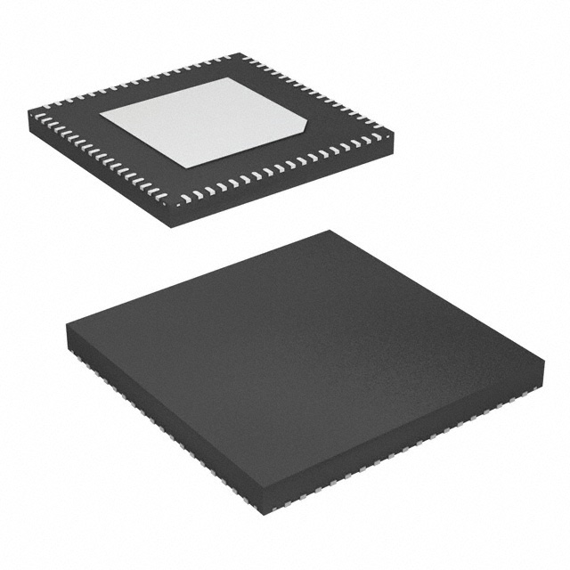


 工商网监
湘ICP备2023018690号
工商网监
湘ICP备2023018690号

